Efficient Energy Funneling in Quasi-2D Perovskites: From Light Emission to Lasing
←
→
Page content transcription
If your browser does not render page correctly, please read the page content below
Communication
                                                                                                                                         www.advmat.de

Efficient Energy Funneling in Quasi-2D Perovskites: From
Light Emission to Lasing
Lei Lei, Dovletgeldi Seyitliyev, Samuel Stuard, Juliana Mendes, Qi Dong, Xiangyu Fu,
Yi-An Chen, Siliang He, Xueping Yi, Liping Zhu, Chih-Hao Chang, Harald Ade,
Kenan Gundogdu, and Franky So*

                                                                                                           high photoluminescence quantum yield
Quasi-2D Ruddlesden–Popper halide perovskites with a large exciton binding                                 (PLQY), wide wavelength tunability, and
energy, self-assembled quantum wells, and high quantum yield draw atten-                                   high color purity,[4–6] they have been attrac-
tion for optoelectronic device applications. Thin films of these quasi-2D                                  tive for light-emitting diode (LED) appli-
perovskites consist of a mixture of domains having different dimensionality,                               cations. Since the first demonstration
                                                                                                           of perovskite LEDs in 2014,[7] the device
allowing energy funneling from lower-dimensional nanosheets (high-bandgap
                                                                                                           external quantum efficiency (EQE) has
domains) to 3D nanocrystals (low-bandgap domains). High-quality quasi-2D                                   risen rapidly from 0.1%[7] to ≈20%,[2,4,8]
perovskite (PEA)2(FA)3Pb4Br13 films are fabricated by solution engineering.                                and the efficiency enhancements are
Grazing-incidence wide-angle X-ray scattering measurements are conducted                                   mainly attributed to passivation and
to study the crystal orientation, and transient absorption spectroscopy meas-                              compositional engineering,[2,8] improved
urements are conducted to study the charge-carrier dynamics. These data                                    charge balance by optimization of device
                                                                                                           structure,[9] and efficient light extrac-
show that highly oriented 2D crystal films have a faster energy transfer from
                                                                                                           tion.[4] More recently, these materials are
the high-bandgap domains to the low-bandgap domains (
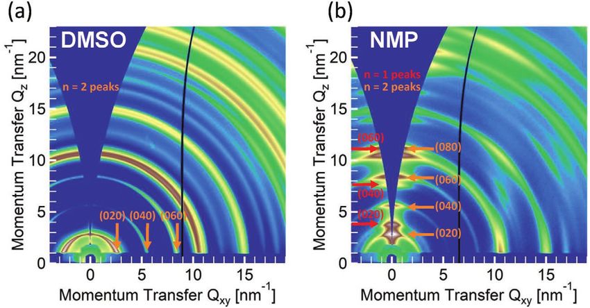
www.advancedsciencenews.com                                                                                               www.advmat.de

domain distribution, it is assumed that the energy rapidly         from high-bandgap domains to low-bandgap domains due
funnels from the high-bandgap domains (donors) to the              to the alignment of the in-plane transition dipole moments,
low-bandgap domains (acceptors) and finally it emits radia-        facilitating an efficient Förster energy transfer. As a result, the
tively in the high-dimensional domains.[20] This process           optimized LED device based on these quasi-2D films resulted
results in rapid charge-carrier localization and increased car-    in a high current efficiency of 41 cd A−1 and EQE of 11.5%.
rier concentration in acceptors, which enhances the bimo-          The same thin films also exhibit a very low ASE threshold of
lecular recombination rate,[21] as well as facilitates the build-  4.16 µJ cm−2. Based on these findings, we further demonstrate
up of population inversion.[22] Therefore, it makes quasi-2D       optically pumped DFB lasers with a low threshold. Our results
perovskites promising for both LED and lasing applica-             show that it is important to control the texture of the quasi-2D
tions. For example, the LEDs based on quasi-2D perovskites         films to achieve efficient energy transfer, which is critical for
recently demonstrated EQE exceeding 15% with PLQY                  optoelectronic devices.
of 70%.[23] Moreover, the outstanding low ASE threshold               The quasi-2D RP-layered perovskites used in this study
of 8.5 µJ cm−2 in 1-naphthylmethylammonium (NMA =                  were fabricated by spin-coating the precursors, which consist
C10H7CH2NH3+)-based quasi-2D perovskites was first demon-          of phenethylammonium bromide (PEABr), formamidinium
strated last year.[22] Since then, there have been several reports bromide (FABr), and lead bromide (PbBr2) with a molar ratio
on ASE and lasing in quasi-2D perovskite materials.[24–26] It is   of 2:3:4. Since the dimensionality of RP-phase perovskites can
demonstrated that a graded domain distribution is favorable        be tuned by adjusting the composition of precursor solutions,
for efficient energy funneling,[27,28] in which the amount         here we focus on the stoichiometry of n = 4 (PEA)2(FA)3Pb4Br13
of low-bandgap acceptors is larger than the high-bandgap           unless otherwise stated. During the spin-coating process, a
donors. Thus, it is able to achieve high quantum yield as well     small amount of antisolvent (chlorobenzene) was dripped onto
as enhanced LED performance. However, a consensus about            the thin films, inducing rapid supersaturation and immediate
how the morphology such as nanocrystal orientation affects         crystallization.[31] In order to tune the morphology of perovskite
the energy transfer process is still lacking. For example, it was  thin films, different precursor solvents are used since it is con-
reported that thin films with randomly oriented crystals exhibit   sidered as an effective way to utilize the solution-based inter-
more efficient charge transport and improved radiative recom-      mediate phase by adjusting the activation energy and growth
bination compared to that of thin films with parallel oriented     kinetics,[32] which is largely affected by the solvent properties
domains in LEDs,[29] and the authors explained that the insu-      such as donor number indicating the coordinating ability of
lating organic layer hindered the charge transfer due to the par-  the Lewis-basic solvents with the Lewis acidic Pb2+ center[33]
allel oriented nanocrystal structure. On the other hand, when      and evaporation rate.[34] In this work, N-methyl-2-pyrrolidone
ASE is compared, the thin films with preferred oriented crystals   (NMP) and dimethyl sulfoxide (DMSO) are chosen as the pre-
exhibited a lower ASE threshold.[30] In contrast, randomly ori-    cursor solvents since they both can be used as a Lewis base to
ented nanocrystals either exhibited ASE at much higher thresh-     form the intermediate phase with lead halides, which results
olds or did not exhibit any ASE,[30] indicating a more efficient   in high-quality perovskite films.[33] However, the differences in
energy funneling in thin films with preferential orientation. So   the evaporation rate, surface wettability, and interaction with
far, the impact of morphology on the energy transfer dynamics      organic cations between DMSO and NMP might lead to the dif-
remains ambiguous. In order to achieve high-quality optoelec-      ference in crystal size and the resulting morphology of quasi-
tronic perovskite devices, it is essential to understand the role  2D perovskite thin films.[34–36]
of morphology in charge and energy transfer kinetics as well as       To study the structure of the films, GIWAXS measure-
to develop methods to control the morphology of the thin films.    ments were done to determine the crystal structure as well as
   In this work, we demonstrate one-step solution-processed        the texture of these perovskite films. As shown in Figure 1, the
phenethylamine (PEA)-based quasi-2D, multi-phasic perovskite       GIWAXS data from an incident angle of 1° show the differences
thin films with a highly efficient energy
transfer rate from the 2D phase to the 3D
phase. In our work, we observed that the effi-
ciency of energy transfer is largely influenced
by the nanocrystal orientation, which can be
efficiently tuned using different precursor
solvents. Via solvent engineering, a high
quality of quasi-2D perovskite films with
preferential orientation is achieved, resulting
in a significant improvement in PL intensity.
The texture of these quasi-2D perovskite thin
films was studied with grazing-incidence
wide-angle X-ray scattering (GIWAXS). The
dynamics of energy transfer was studied by
time-resolved absorption spectroscopy (TAS),
revealing a more efficient energy funneling
process in the well-oriented thin films. We Figure 1. a,b) GIWAXS patterns of the spin-cast perovskite films from solvent DMSO (a) and
propose that highly oriented domains are NMP (b). Unique peaks from an n = 2 layered perovskite phase are indicated by orange indices/
beneficial for efficient energy funneling arrows, while those from n = 1 are in red.

Adv. Mater. 2020, 32, 1906571                             1906571 (2 of 9)              © 2020 WILEY-VCH Verlag GmbH & Co. KGaA, Weinheim
www.advancedsciencenews.com www.advmat.de between the two thin films. The film made by DMSO shows respectively, due to the quantum confinement effects.[5] The long arcs of intensity in the GIWAXS pattern indicating that absorbance spectra of the quasi-2D perovskite film prepared by the crystallites are isotropically distributed without any pre- the DMSO solvent show a strong absorption peak at 434 nm, ferred orientation.[37] In contrast, the pattern from the NMP indicating that the major component of the perovskite film is film displays sharp peaks with short arc lengths along the the n = 2 domains. The weak absorption peak at 460 nm shows Qz-axis. These scattering points are indicative of a strongly tex- the existence of the n = 3 domains, and the presence of the n = 1 tured, preferentially oriented film. Previous work showed that domains is almost negligible. However, in the NMP film, the thin films of stoichiometric n = 4 layered perovskites contain relatively even and small excitonic absorption peaks at 401 mixed phases of n = 1, 2, 3 layered perovskite as well as the cor- and 434 nm indicate a similar fraction of the n = 1 and n = 2 responding 3D phase, such as (FA)PbI3.[38] Because of the large domains. The signals for n ≥ 4 domains are not visible in the spacing (created by organic spacer molecules like PEA) between absorption spectrum. For both samples, the band edge absorp- the strong scattering lead-iodide layers in layered perovskites, tion of 3D domains appears as shoulders at around 530 nm, only layered perovskite phases (and not the bulk phase) can indicating a mixture of 2D and 3D domains. The PL spectra generate scattering momentum transfers less than 10 nm−1 for the perovskite films prepared by different solvents are (since there is an inverse relationship between real spacing plotted in Figure S5b (Supporting Information). It is clear that and reciprocal spacing).[39] In the present DMSO pattern, three a stronger emission is observed in the perovskite film prepared scattering signatures at less than 10 nm−1 are noticeable. Using using NMP, indicating reduced nonradiative recombination indexGIXS software to fit these low-Q peaks to the expected scat- centers. It is worth mentioning that a slight blue-shift of emis- tering from several potential-layered perovskite unit cells, the sion peak is observed in the NMP sample, which is consistent three peaks were identified as being generated from the family with the XRD data indicating a reduction of the crystal size in of (0k0) planes in the n = 2 layered perovskite.[40] As seen in the the 3D domains. pattern, the arc from the diffraction signal is close to isotropic, We further carried out ultrafast TAS measurements to get a indicating that the lead-bromide sheets of n = 2 oriented ran- deeper insight into the transfer dynamics of photocarriers and domly having a slightly perpendicular (“edge-on”) orientation thereby reveal the difference between the two quasi-2D films in the films. The n = 2 scattering signal is also present in the prepared by NMP and DMSO. The representative 2D maps of NMP sample, but in a very different way. As clearly indicated the transient absorption spectra with an excitation wavelength on the pattern, the same (0k0) family of peaks is now shown of 355 nm are shown in Figure S6 (Supporting Information). on the Qz-axis. The sharp intensity of these peaks as well as Here, the change in transmittance is showed as a color height- the short arc length means that the lead-bromide sheets in this map as a function of wavelength and pump delay. We further sample are parallel to the substrate. Similarly, an n = 1 (0k0) extract the evolution of the transient absorption spectra at early family of peaks is also present in the in-plane orientation. time delays as shown in Figure 2a,b. Several bleaching features There are not many differences between the GIWAXS data are present, and the decay kinetics coincide with the features from different incident angles of 0.15° (Figure S1, Supporting of energy transfer reported previously.[20] For both NMP and Information) and 1°, indicating good uniformity of nanostruc- DMSO films, the initial photoexcitation is formed on the low- tures along the vertical direction of the films. These observa- dimensional domains, evidenced by the ground state bleaching tions are consistent with the X-ray diffraction (XRD) patterns (GSB) feature at ≈430 nm, which is in agreement with the peak (Figure S2, Supporting Information). A family of (0k0) planes position of n = 2 domain from the steady-state absorption spec- in n = 1 and n = 2 layered perovskites is clearly observed in trum (Figure S5a, Supporting Information). The bleaching the NMP film. In contrast, very weak peak intensity is observed features at lower energy can be assigned as the GSB signals of in the n = 2 layered DMSO perovskite sample. Moreover, com- higher dimensional perovskite domains, and the corresponding pared to the film made from DMSO, a broader peak at 14.9° in n values are marked. Upon excitation, the photoexcited carrier the NMP film indicates the reduction of 3D nanocrystal size, population in the high-dimensional domains rises as the popu- which promotes bimolecular radiative recombination.[6] The lation decays in the low-dimensional domains, indicating the surface morphology of the perovskite thin films is observed energy funneling from the high-bandgap domains to the lower- by scanning electronic microscopy (SEM) and atomic force bandgap 3D domains. In both thin films, the n = 2 domain pop- microscopy (AFM). As shown in the SEM images (Figure S3, ulation decays in < 1 ps initially with the remaining bleaching Supporting Information), thin films with uniform surface cov- signal lasting for a long time period (≈1000 ps). This suggests erage are obtained for all samples. Fewer features are present in that charge carriers are accumulated in the n = 2 domains the film made with the NMP solvent than the DMSO solvent, and the energy transfer is incomplete which is supported by indicating a smoother surface. AFM measurements (Figure S4, the time-resolved PL (TRPL) decays at 440 nm in Figure S7a Supporting Information) also confirm that a decrease of rough- (Supporting Information). However, by comparing spectral ness is observed in the NMP sample compared to the DMSO line shapes in Figure 2a,b for the DMSO and NMP samples, it sample. clearly shows a larger population of carriers remaining in the The optical properties of quasi-2D perovskites are largely 2D domains for the DMSO indicating an incomplete energy affected by the texture and morphology. Figure S5a (Supporting transfer. Extracting the domain distribution information from Information) shows the UV–vis spectra for thin films pre- the absorbance spectra and TAS data, we conclude that the pared by DMSO and NMP. According to previous reports of acceptor (3D domains) to donor (2D domains) ratio is larger in PbBr4-based quasi-2D perovskites, the absorption peaks at 401 the NMP film than the DMSO film. This higher acceptor con- and 434 nm are assigned to the n = 1 and n = 2 domains,[29,41] centration could be the reason for more complete and efficient Adv. Mater. 2020, 32, 1906571 1906571 (3 of 9) © 2020 WILEY-VCH Verlag GmbH & Co. KGaA, Weinheim
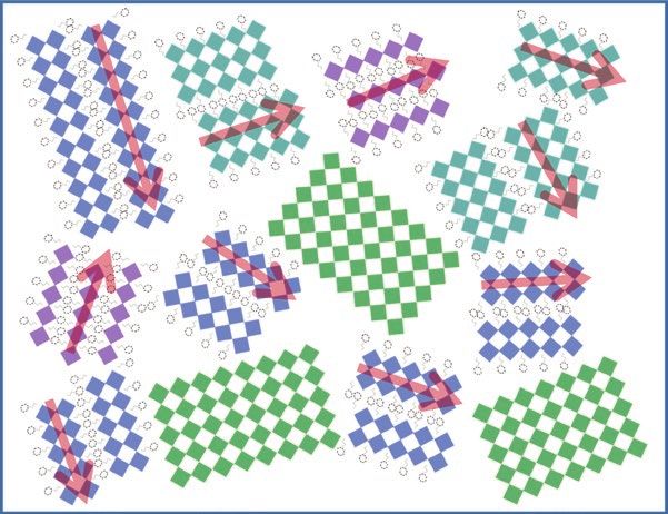
www.advancedsciencenews.com                                                                                                             www.advmat.de

Figure 2. a,b) Transient absorption spectra at various delay times of the perovskite films from solvent DMSO (a) and NMP (b), and c,d) de-convolved
dynamics of photobleaching features at n = 2, n = 3, n ≥ 4 and 3D phases for DMSO (c) and NMP (d) samples. The black curves represent the best fit
obtained for the corresponding dynamics. e,f) Schematic of illustrations of quasi-2D perovskite with random orientation (e) and preferential orientation
(f). The arrows indicate the transition dipole orientation in nanocrystals.

energy transfer due to less trapped population in the NMP                     same timescale.[20] The data show a similar trend for the thin
film.[27,28]                                                                  film made from NMP, whereas the n ≥ 4 domains are not vis-
   In order to further study the energy transfer dynamics from                ible in the TAS signal. It should be noted that the rising time
the higher energy domains to the lower energy 3D perovskite                   of the 3D domain is about 0.13 ps for the NMP sample, which
domains, we de-convolved the spectra and plotted the evolu-                   is significantly faster than the 3D domain dynamics observed
tion of each domain signal as a function of time in Figure 2c,d.              (0.36 ps) for the DMSO sample, indicating that photocarriers
The fitting of the dynamics of photobleaching at different                    relaxed to the 3D domain in the NMP sample are faster than
wavelengths is shown in Figure 2c,d, and the results are sum-                 that in the DMSO sample. This fast exciton capture time in
marized in Table S1 (Supporting Information). In the DMSO                     the 3D domains for the NMP sample within 0.13 ps is faster
sample, upon the initial excitation, the population in the n = 2              than the 10–100 ps energy transfer rate reported previously,[5,20]
and n = 3 domains showed a relaxation with a similar decay                    suggesting that this faster energy transfer rate is due to the
time constant (≈0.3 ps), and the n ≥ 4 domains showed a faster                highly oriented nanocrystal structures provided by the NMP
rise time (0.2 ps) indicating a built-up of photocarriers fol-                solvent. Energy transfer can happen as a radiative transfer or
lowed by a slower decay (0.4 ps). In addition, the rise time for              nonradiative transfer such as Förster resonance energy transfer
the 3D domains is 0.36 ps, which further supports the accu-                   (FRET) and Dexter exchange energy transfer from a donor to
mulation of excitons in the 3D domains is dominated by the                    an acceptor.[42] Since the thickness of the insulating interca-
energy transfer from the high-bandgap domains (low n-value                    lating organic layer is larger than 1 nm,[43] the energy transfer
phase) to the low-bandgap domains (3D perovskites) within the                 from the 2D to the 3D domains is more likely due to FRET,

Adv. Mater. 2020, 32, 1906571                                     1906571 (4 of 9)                 © 2020 WILEY-VCH Verlag GmbH & Co. KGaA, Weinheim
www.advancedsciencenews.com www.advmat.de
which depends on the overlap of the donor emission and faster radiative recombination rate via more efficient energy
acceptor absorption spectra, the transition dipole orientation transfer. The devices with two different solvents give the
and the donor–acceptor separation.[28,44–46] In the NMP sample, same electroluminescence (EL) peaks at 525 nm as shown in
oriented crystal gives a higher density,[30] along with a smaller the inset of Figure 3b. Both devices show good repeatability,
spacing between the domains. Thus, the decreased donor– as EQE histogram among ≈25 devices as shown in Figure S8
acceptor spacing gives rise to a higher energy transfer effi- (Supporting Information). The best performing device with the
ciency. Moreover, the band structure calculations have predicted DMSO film yields a CE of 32 cd A−1, while an LED device with
that the transition dipole moments are inclined to orient along NMP processed film shows as high as 41 cd A−1 resulting in
the nanosheet direction in 2D perovskites,[47] which also have an EQE of 11.5%. This efficiency enhancement is attributed to
been confirmed by the anisotropic exciton response observed the high quality of the quasi-2D perovskite film with a smooth
experimentally.[43,48] Therefore, it is proposed that the highly surface, high crystallinity, as well as highly oriented nanocrys-
oriented low-dimensional domains in the NMP samples give tals, which gives a more efficient energy transfer and radiative
a preferential transition dipole orientation (mostly parallel to recombination.
the substrate), which also makes the energy transfer more effi- To investigate whether an efficient energy transfer between
cient.[44] Hence, we hypothesize that the quasi-2D perovskites the domains leads to low ASE threshold, we use a 150 fs pulse
films introduced by NMP solvent with a faster energy transfer laser having a repetition rate of 1 kHz to excite the quasi-2D
are caused by enhanced FRET efficiency due to the decreased perovskite thin films on quartz substrate. The laser excita-
donor–acceptor distance and the aligned dipole orientation tion wavelength is 400 nm and the excitation spot is 4.5 mm
between crystals. The schematic of the proposed mechanism is in diameter. Figure 4a,b shows the pump fluence–dependent
shown in Figure 2e,f. PL spectra for films prepared from DMSO and NMP solvents,
To demonstrate the importance of efficient energy transfer respectively. At low pump fluences, the spontaneous emission
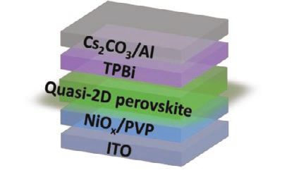
from the quasi-2D domains to the 3D domains, LEDs (SE) spectrum is centered at 537 nm with a full-width at half-
were fabricated using on these quasi-2D perovskite films. maximum (FWHM) of 28 nm. When the pump fluence exceeds
A device structure of indium tin oxide (ITO)/nickel oxide the ASE threshold, a narrower bandwidth (≈4 nm) ASE peak
(NiOx)/poly(vinylpyrrolidone) (PVP)/quasi-2D perovskites/2′,2′- appears at 542 nm. In the intensity–pump fluence plot, the
(1,3,5-benzinetriyl)-tris(1-phenyl-1-H-benzimidazole) (TPBi)/ ASE threshold is represented as a sharp increase in the slope.
Cs2CO3/Al is used and the schematic diagram is shown in the The ASE threshold of the NMP sample (4.16 µJ cm−2) is one
inset of Figure 3a. Here, an ultrathin layer of PVP is used to order lower than that of the DMSO sample (51.08 µJ cm−2) and
passivate the surface of NiOx in order to suppress the exciton the data are shown in Figure 4c,d. To determine the threshold
quenching as previously reported.[49] The current density– carrier density N, the equation is used: N = α Pλ .[22] Here, P is
hc
voltage–luminescence and the current efficiency–current den- the measured ASE threshold power fluence, λ is the excita-
sity characteristics are plotted in Figure 3a,b, respectively. From tion wavelength, h is the Planck’s constant, c is the light speed
the current density versus voltage (J–V) curves, a slight decrease in vacuum, and α is the absorption coefficient (for the
of the current density is observed at voltages above 4 V for the DMSO sample, α = 1.4 × 105 cm−1 and for the NMP sample,
device having a perovskite layer using NMP as a solvent. This α = 1.7 × 105 cm−1 at 400 nm from the UV–vis measurements).
decrease in current density may be due to the insulating organic As a result, the threshold carrier density for the DMSO sample
layer parallel to the substrate-impeding charge transport. On is determined to be 1.5 × 1019 cm−3, one order of magnitude
the other hand, there is no significant difference in the turn-on higher than the NMP sample at 1.4 × 1018 cm−3. By com-
voltage (3 V) in devices with films processed using both solvents paring the TRPL decays for both DMSO and NMP samples in
indicating that the parallel-oriented quasi-2D perovskite films Figure S7 (Supporting Information), no significant difference
does not affect carrier injection. However, the LED devices based of PL lifetime is observed, suggesting that the defect passivation
on the NMP film yield a higher luminescence at 7 V (Figure 3a) effect is not obvious in the NMP sample. Therefore, the lower
and an enhanced current efficiency (CE; Figure 3b) due to the threshold in the NMP sample is attributed to a faster energy
(a) 105 (b) 60
Normalized EL
DMSO
Current Density (mA/cm2)
DMSO
Current Efficiency (cd/A)
1
10
Luminance(cd/m2)
NMP
104 50 NMP
103 40
10-1 450 500 550 600
2
10 30 Wavelength (nm)
101 20
10-3
0
10 10
10-5 10-1
0 1 2 3 4 5 6 7 0 2 4 6 8 10
Voltage (V) Current Density (mA/cm2)
Figure 3. Device performance of PeLEDs. a) J–V–L data (inset shows the device structure), b) current efficiency (EL shown in the inset) of the devices
based on perovskite films prepared from NMP and DMSO solvents, respectively.
Adv. Mater. 2020, 32, 1906571 1906571 (5 of 9) © 2020 WILEY-VCH Verlag GmbH & Co. KGaA, Weinheim
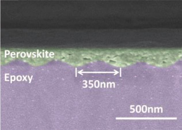
www.advancedsciencenews.com www.advmat.de Figure 4. ASE for quasi-2D perovskite thin films. a,b) Pump-fluence dependence of the emission on perovskite thin films prepared from DMSO (a) and NMP (b) with the excitation laser (400 nm, 150 fs pulses), respectively. c,d) ASE threshold is measured by PL intensity versus pump fluence at ASE peak (≈542 nm) for DMSO (c) and NMP (d) samples, where DMSO shows threshold of 51.08 µJ cm−2 and NMP shows threshold of 4.16 µJ cm−2. funneling process than the DMSO sample, leading to a faster good spatial coherence using oriented crystal perovskite thin films. population inversion build-up in the low-bandgap domains.[22] Further improvements need to be done to enhance the perovskite The lower threshold carrier density for the NMP sample indi- emission characteristics by optimizing the grating structure.[15] cates a possibility of attaining a gain from optical pumping.[10] In summary, we demonstrate quasi-2D RP perovskite films To demonstrate lasing in the low ASE threshold quasi-2D prepared via a simple solution process which exhibits desir- perovskite thin film processed with the NMP solvent by optical able optical properties for high-efficiency LEDs and low ASE pumping, a DFB laser having a 1D grating (period Λ = 350 nm) threshold. The perovskite nanocrystal orientation is strongly was fabricated. To fabricate a DFB laser, the grating substrate affected by different precursor solvents, DMSO and NMP. By was fabricated by interference lithography (IL) and nanoim- using NMP as precursor solvent, quasi-2D perovskite crystals printing, followed by spin coating of a 100 nm thick layer of with a strong preferred orientation can be achieved, while the spin-coated perovskite on the grating. Note the grating has DMSO solvent results quasi-2D perovskite crystals with random relatively large features and low aspect ratio compare with the orientation. These highly oriented perovskite films show a nanocrystals and is not expected to change the morphology of more efficient energy transfer due to the preferred transition the perovskite films. The SEM cross-section of the DFB laser dipole orientation and decreased donor–acceptor distance. This is shown in Figure 5a. The perovskite film thickness is chosen understanding of perovskite nanocrystal orientation sheds to support only the fundamental transverse electric (TE0) light on the requirements for light-emitting devices. Using the waveguide mode. While the second-order Bragg diffraction of optimized quasi-2D perovskite films, we demonstrated a high- the grating creates the optical resonance at the ASE wavelength, efficiency LED device with a CE of 41 cd A−1, corresponding to the first-order Bragg diffraction diffracts the waveguide mode an EQE of 11.5%. We further demonstrate a low ASE threshold into the surface normal as the laser output.[50] The sample was of 4.16 µJ cm−2 and a green emission DFB laser based on the optically pumped at room temperature using the same optimized perovskite thin films. Our results demonstrate an pulsed optical pumping as the ASE setup. As the pump flu- effective method to obtain good-quality quasi-2D, multiphasic ence increases, a clear emission power threshold is observed at perovskite thin films for LED and laser applications. 10 µJ cm−2 (Figure 5b). Above the threshold, we observe the lasing emission with the line-narrowing (FWHM of 1.7 nm, as shown in Figure 5c) and a linear laser emission pattern corresponding to the width of the excitation spot (Figure 5b Experimental Section inset). The lasing emission is strongly TE polarized, which Material Preparation: The (PEA)2(FA)3Pb4Br13 precursors were is consistent with the characteristics of the DFB lasers,[51] prepared by dissolving PEABr, FABr, PbBr2 (2:3:4 molar ratio) and demonstrating a green DFB laser having a low threshold and MACl (0.05 mmol) in 1 mL anhydrous NMP or DMSO solvent to make Adv. Mater. 2020, 32, 1906571 1906571 (6 of 9) © 2020 WILEY-VCH Verlag GmbH & Co. KGaA, Weinheim
www.advancedsciencenews.com                                                                                                           www.advmat.de

Figure 5. DFB laser based on quasi-2D perovskites thin films with well-oriented domains. a) SEM cross-section of DFB lasers with a period of 350 nm
and quasi-2D perovskite thin films with a thickness of 100 nm. b) Lasing threshold measurement of DFB laser. The inset is the photograph of far-field
lasing emission projected on white paper. c) PL emission measured from the planar thin film and lasing emission measured from the surface of device
containing DFB gratings pumped with 400 nm 150 fs laser. The polarization of lasing emission is shown in the inset.

0.5 m (Pb2+ concentration) solutions. The solutions were stirred for 2 h    using the above method. Finally, the fabricated devices were sealed in
at 60 °C in a glovebox with a nitrogen environment.                         glovebox by UV-curable resin before testing.
   The NiOx solution precursor was synthesized according to the previous       Material and LED Device Characterization: XRD measurements
publication.[49] Nickel acetate tetrahydrate (Ni(CH3COO)2 · 4H2O) and       were carried out with Rigaku Smartlab X-ray Diffractometer with a
ethanolamine(NH2CH2CH2OH) were dissolved in ethanol (0.1 mol L−1)           conventional Cu X-ray tube. Steady-state PL spectra of perovskite films
with a molar ratio of 1:1, and stirred at 65 °C for 1 h.                    were measured with an Edinburgh Instruments FS920 fluorimeter that
   Fabrication of Perovskite LEDs: The prepatterned ITO-coated glass        was equipped with a 450 W Xe arc lamp for excitation source and a
substrates were used to fabricate the LEDs. First, the substrates were      Peltier-cooled Hammamatsu R2658P photomultiplier tube (PMT). The
cleaned in acetone and isopropanol for 15 min in sequence, and              excitation wavelength was 375 nm. Nanosecond TRPL spectra were
then dried by N2. The cleaned substrates were UV-ozone treated for          collected on an LP 920 spectrometer from Edinburgh Instruments with
15 min. NiOx as the hole injection layer was prepared by spin-coating       the excitation of 390 nm. The UV–vis absorbance spectra were recorded
NiOx precursor at 2000 rpm for 40 s and baked at 500 °C for 1 h             on an UV–vis spectrophotometer (Lambda 750, PerkinElmer). SEM
in ambient air. Then the substrates were transferred into a glovebox.       images of the perovskite films were collected in FEI Verios 460L. The
An ultrathin passivation layer was spin-coated by PVP (4 mg mL−1)           J–V–L characterization was obtained by using Keithley 2400 sourcemeter.
in dimethylformamide at 5000 rpm for 30 s, and annealed at                     ASE and Lasing Characterization: For ASE and lasing spectra
120 °C for 10 min. Thereafter, the perovskite solution was spin-coated      measurements, samples were pumped by 400 nm pulsed laser which
onto the NiOx films at 3000 rpm for 2 min, during which time (at            was obtained from second harmonic generation of the 800 nm 150 fs
28 s for DMSO and 31 s for NMP) chlorobenzene (150 µL) was                  output from Quantronix Integra-C laser. The pulse width was 150 fs,
dripped onto the surface, followed by annealing at 90 °C for 10 min.        the repetition was 1 kHz, and the spot size was 4.5 mm in diameter.
The as-prepared substrates were then transferred into a thermal             Resulting emission was recorded by the charge-coupled device (CCD)
evaporator, and 40 nm TPBi, 2 nm Cs2CO3, and 100 nm Al were                 spectrometer from Mightex Systems. All spectroscopy measurements
deposited layer by layer. The device area was defined by the area of        were carried out in air.
overlap of ITO anode and Al cathode 4 mm2 (2 × 2 mm). Finally, the             GIWAXS: Films were spin-cast on silicon substrates in preparation for
fabricated devices were sealed in glovebox by ultraviolet-curable resin     the GIWAXS measurements. GIWAXS was conducted on each sample
before testing.                                                             in a He atmosphere at beamline 7.3.3 at the Advanced Light Source
   Fabrication of DFB Laser: The DFB cavity was fabricated by using         (ALS) in Lawrence Berkeley National Lab (LBNL).[52] The incident photon
nanoimprinting lithography from a silicon master nanostructure. The         energy was 10 keV at an incident angle of 1o and the scattered photons
nanostructures on silicon molds were patterned using IL and transferred     were collected by a Pilatus 2M detector. Patterns were processed,
using reactive ion etching (RIE). First, a 100 nm antireflection coating    corrected, analyzed, and colored in a modified NIKA package of Igor
(ARC) and 180 nm positive photoresist (PR) were spin-coated on silicon      Pro.[53] A logarithmic color scale was used for each pattern. The software
substrate. The ARC film was used to reduce the reflection from the          indexGIXS 2.0, CrystalMaker 10.2.2, and CrystalDiffract 6.7.3 were used
substrate during lithography. The 1D periodic grating in PR was then        to help index peaks in the GIWAXS patterns.[40]
patterned using 325 nm wavelength HeCd laser exposure in a Lloyd’s             TAS: Transient absorption data were collected using TAS setup. This
mirror IL setup, where two coherent laser beams interfered to create        setup was consisted of the spectrometer (Ultrafast Helios system) and
periodic intensity pattern. Then, the 1D pattern was transferred to the     amplified Ti:Saphhire laser. The output of amplified Ti:Saphhire laser
underlying silicon substrate using O2 and Cl2 RIE. After etching, an        provided 800 nm fundamental pulses at 1 kHz repetition rate which were
RCA (the Radio Corporation of America) cleaning process was used to         split into two optical beams to generate pump and probe pulses. One
remove the organic contaminants on the substrate surface. The surfaces      fundamental beam was used to generate pump beam using an optical
of the molds were then treated with silane to mitigate adhesion for the     parametric amplifier system (Coherent Opera Solo). A white light/
subsequent nanoimprint process.                                             near-infrared probe was generated by focusing another fundamental
   For nanoimprint lithography, first a poly(dimethylsiloxane) stamp        beam into a flint glass. Pump and probe beams were focused on a
was cast from a silicon master structure (cured by 90 °C for 2 h) and       sample and probe light was collected by a CCD device. The spectral
subsequently used to nanoimprint into a grating structure on a spin-        detection region was 350–600 nm. The thin-film samples were prepared
coated epoxy films (cured under UV exposure). The resultant grating         on glass substrates and encapsulated using UV curable glue before
structure was then UV-ozone treated for 30 min to improve wettability,      measurement. The instrument response function was ≈100 fs FWHM.
and the perovskite precursor was spin coated on top of the sample           The samples were excited with the excitation wavelength of 355 nm and

Adv. Mater. 2020, 32, 1906571                                    1906571 (7 of 9)                © 2020 WILEY-VCH Verlag GmbH & Co. KGaA, Weinheim
www.advancedsciencenews.com                                                                                                             www.advmat.de

the fractional change in transmission was detected in the probe range         [6] Z. Xiao, R. A. Kerner, L. Zhao, N. L. Tran, K. M. Lee, T.-W. Koh,
350–600 nm at several time delays.                                                G. D. Scholes, B. P. Rand, Nat. Photonics 2017, 11, 108.
                                                                              [7] Z. Tan, R. S. Moghaddam, M. L. Lai, P. Docampo, R. Higler,
                                                                                  F. Deschler, M. Price, A. Sadhanala, L. M. Pazos, D. Credgington,
                                                                                  F. Hanusch, T. Bein, H. J. Snaith, R. H. Friend, Nat. Nanotechnol.
Supporting Information                                                            2014, 9, 687.
Supporting Information is available from the Wiley Online Library or          [8] B. Zhao, S. Bai, V. Kim, R. Lamboll, R. Shivanna, F. Auras,
from the author.                                                                  J. M. Richter, L. Yang, L. Dai, M. Alsari, X. She, L. Liang,
                                                                                  J. Zhang, S. Lilliu, P. Gao, H. J. Snaith, J. Wang, N. C. Greenham,
                                                                                  R. H. Friend, D. Di, Nat. Photonics 2018, 12, 783.
                                                                              [9] Y. Zou, M. Ban, Y. Yang, S. Bai, C. Wu, Y. Han, T. Wu, Y. Tan,
Acknowledgements                                                                  Q. Huang, X. Gao, T. Song, Q. Zhang, B. Sun, ACS Appl. Mater.
                                                                                  Interfaces 2018, 10, 24320.
The authors are thankful for the support from the National Science
Foundation DMREF Program (NSF Award #1729383) and the UNC                    [10] G. Xing, N. Mathews, S. S. Lim, N. Yantara, X. Liu, D. Sabba,
Research Opportunities Initiative Center for Hybrid Materials Enabled             M. Grätzel, S. Mhaisalkar, T. C. Sum, Nat. Mater. 2014, 13, 476.
Electronic Technologies (CHMEET). The GIWAXS data were acquired at           [11] P. Chhantyal, S. Naskar, T. Birr, T. Fischer, F. Lübkemann,
beamline 7.3.3 at the ALS in Lawrence Berkeley National Laboratory,[52]           B. N. Chichkov, D. Dorfs, N. C. Bigall, C. Reinhardt, Sci. Rep. 2018,
which is supported by the U.S. Department of Energy (no. DE-AC02-                 8, 3962.
05CH11231). Experimental support was provided at the ALS by beamline         [12] H. Nakanotani, S. Akiyama, D. Ohnishi, M. Moriwake, M. Yahiro,
scientists C. Zhu and A. Liebman-Pelaez. H.A. and S.S. are supported              T. Yoshihara, S. Tobita, C. Adachi, Adv. Funct. Mater. 2007, 17, 2328.
by UNC-GA Research Opportunity Initiative (ROI) grant. Work by               [13] F. Deschler, M. Price, S. Pathak, L. E. Klintberg, D.-D. Jarausch,
C.-H.C. is supported by the National Science Foundation (NSF) grant               R. Higler, S. Hüttner, T. Leijtens, S. D. Stranks, H. J. Snaith,
CMMI#1552424. The part of the work (XRD and SEM) was performed                    M. Atatüre, R. T. Phillips, R. H. Friend, J. Phys. Chem. Lett. 2014, 5,
in the Analytical Instrumentation Facility (AIF) at North Carolina State          1421.
University, which is supported by the State of North Carolina and the        [14] S. Chen, C. Zhang, J. Lee, J. Han, A. Nurmikko, Adv. Mater. 2017,
National Science Foundation (award number ECCS-1542015). The AIF                  29, 1604781.
is a member of the North Carolina Research Triangle Nanotechnology           [15] Z. Li, J. Moon, A. Gharajeh, R. Haroldson, R. Hawkins, W. Hu,
Network (RTNN), a site in the National Nanotechnology Coordinated                 A. Zakhidov, Q. Gu, ACS Nano 2018, 12, 10968.
Infrastructure (NNCI).
                                                                             [16] A. Zhizhchenko, S. Syubaev, A. Berestennikov, A. V. Yulin,
                                                                                  A. Porfirev, A. Pushkarev, I. Shishkin, K. Golokhvast, A. A. Bogdanov,
                                                                                  A. A. Zakhidov, A. A. Kuchmizhak, Y. S. Kivshar, S. V. Makarov, ACS
                                                                                  Nano 2019, 13, 4140.
Conflict of Interest
                                                                             [17] H. Zhang, Y. Wu, Q. Liao, Z. Zhang, Y. Liu, Q. Gao, P. Liu, M. Li,
The authors declare no conflict of interest.                                      J. Yao, H. Fu, Angew. Chem., Int. Ed. 2018, 57, 7748.
                                                                             [18] T. Ishihara, X. Hong, J. Ding, A. V. Nurmikko, Surf. Sci. 1992, 267,
                                                                                  323.
                                                                             [19] L. N. Quan, M. Yuan, R. Comin, O. Voznyy, E. M. Beauregard,
Keywords                                                                          S. Hoogland, A. Buin, A. R. Kirmani, K. Zhao, A. Amassian,
amplified spontaneous emission, distributed-feedback lasers, energy               D. H. Kim, E. H. Sargent, J. Am. Chem. Soc. 2016, 138, 2649.
funneling, light-emitting diodes, quasi-2D perovskites                       [20] M. Yuan, L. N. Quan, R. Comin, G. Walters, R. Sabatini, O. Voznyy,
                                                                                  S. Hoogland, Y. Zhao, E. M. Beauregard, P. Kanjanaboos, Z. Lu,
                                               Received: October 7, 2019          D. H. Kim, E. H. Sargent, Nat. Nanotechnol. 2016, 11, 872.
                                                Revised: January 16, 2020    [21] G. Xing, B. Wu, X. Wu, M. Li, B. Du, Q. Wei, J. Guo, E. K. L. Yeow,
                                      Published online: February 28, 2020         T. C. Sum, W. Huang, Nat. Commun. 2017, 8, 14558.
                                                                             [22] M. Li, Q. Gao, P. Liu, Q. Liao, H. Zhang, J. Yao, W. Hu, Y. Wu,
                                                                                  H. Fu, Adv. Funct. Mater. 2018, 28, 1707006.
                                                                             [23] M. Ban, Y. Zou, J. P. H. Rivett, Y. Yang, T. H. Thomas, Y. Tan,
 [1] G. Hodes, Science 2013, 342, 317.                                            T. Song, X. Gao, D. Credgington, F. Deschler, H. Sirringhaus,
 [2] K. Lin, J. Xing, L. N. Quan, F. P. G. de Arquer, X. Gong, J. Lu,             B. Sun, Nat. Commun. 2018, 9, 3892.
     L. Xie, W. Zhao, D. Zhang, C. Yan, W. Li, X. Liu, Y. Lu, J. Kirman,     [24] M. R. Leyden, S. Terakawa, T. Matsushima, S. Ruan, K. Goushi,
     E. H. Sargent, Q. Xiong, Z. Wei, Nature 2018, 562, 245.                      M. Auffray, A. S. D. Sandanayaka, C. Qin, F. Bencheikh, C. Adachi,
 [3] M. Saliba, S. M. Wood, J. B. Patel, P. K. Nayak, J. Huang,                   ACS Photonics 2019, 6, 460.
     J. A. Alexander-Webber, B. Wenger, S. D. Stranks, M. T. Hörantner,      [25] H. Zhang, Q. Liao, Y. Wu, Z. Zhang, Q. Gao, P. Liu, M. Li, J. Yao,
     J. T. Wang, R. J. Nicholas, L. M. Herz, M. B. Johnston, S. M. Morris,        H. Fu, Adv. Mater. 2018, 30, 1706186.
     H. J. Snaith, M. K. Riede, Adv. Mater. 2016, 28, 923.                   [26] M. R. Leyden, T. Matsushima, C. Qin, S. Ruan, H. Ye, C. Adachi,
 [4] Y. Cao, N. Wang, H. Tian, J. Guo, Y. Wei, H. Chen, Y. Miao, W. Zou,          Phys. Chem. Chem. Phys. 2018, 20, 15030.
     K. Pan, Y. He, H. Cao, Y. Ke, M. Xu, Y. Wang, M. Yang, K. Du, Z. Fu,    [27] L. N. Quan, Y. Zhao, F. P. García de Arquer, R. Sabatini, G. Walters,
     D. Kong, D. Dai, Y. Jin, G. Li, H. Li, Q. Peng, J. Wang, W. Huang,           O. Voznyy, R. Comin, Y. Li, J. Z. Fan, H. Tan, J. Pan, M. Yuan,
     Nature 2018, 562, 249.                                                       O. M. Bakr, Z. Lu, D. H. Kim, E. H. Sargent, Nano Lett. 2017, 17,
 [5] N. Wang, L. Cheng, R. Ge, S. Zhang, Y. Miao, W. Zou, C. Yi,                  3701.
     Y. Sun, Y. Cao, R. Yang, Y. Wei, Q. Guo, Y. Ke, M. Yu, Y. Jin,          [28] N. Yantara, A. Bruno, A. Iqbal, N. F. Jamaludin, C. Soci,
     Y. Liu, Q. Ding, D. Di, L. Yang, G. Xing, H. Tian, C. Jin, F. Gao,           S. Mhaisalkar, N. Mathews, Adv. Mater. 2018, 30, 1800818.
     R. H. Friend, J. Wang, W. Huang, Nat. Photonics 2016, 10,               [29] H. Lee, H. Kim, H. Cho, W. Cha, Y. Hong, Y. Kim, A. Sadhanala,
     699.                                                                         V. Venugopalan, J. S. Kim, J. W. Choi, C. Lee, D. Kim,

Adv. Mater. 2020, 32, 1906571                                     1906571 (8 of 9)                 © 2020 WILEY-VCH Verlag GmbH & Co. KGaA, Weinheim
www.advancedsciencenews.com www.advmat.de
H. Yang, R. H. Friend, T. Lee, Adv. Funct. Mater. 2019, 29, [40] D. Smilgies, D. R. Blasini, J. Appl. Crystallogr. 2007, 40, 716.
1901225. [41] X. Yang, X. Zhang, J. Deng, Z. Chu, Q. Jiang, J. Meng, P. Wang,
[30] R. Wang, Y. Tong, A. Manzi, K. Wang, Z. Fu, E. Kentzinger, L. Zhang, Z. Yin, J. You, Nat. Commun. 2018, 9, 570.
J. Feldmann, A. S. Urban, P. Müller-Buschbaum, H. Frielinghaus, [42] M. A. Omary, H. H. Patterson, in Encyclopedia of Spectro
Adv. Opt. Mater. 2018, 6, 1701311. scopy and Spectrometry, 3rd ed. (Eds: J. C. Lindon, G. E. Tranter,
[31] M. Xiao, F. Huang, W. Huang, Y. Dkhissi, Y. Zhu, J. Etheridge, D. W. Koppenaal), Academic Press, 2017, pp. 636–653.
A. Gray-Weale, U. Bach, Y. B. Cheng, L. Spiccia, Angew. Chem., Int. [43] A. Fieramosca, L. De Marco, M. Passoni, L. Polimeno, A. Rizzo,
Ed. 2014, 53, 9898. B. L. T. Rosa, G. Cruciani, L. Dominici, M. De Giorgi, G. Gigli,
[32] Y. Jo, K. S. Oh, M. Kim, K.-H. Kim, H. Lee, C.-W. Lee, D. S. Kim, Adv. L. C. Andreani, D. Gerace, D. Ballarini, D. Sanvitto, ACS Photonics
Mater. Interfaces 2016, 3, 1500768. 2018, 5, 4179.
[33] J. C. Hamill, J. Schwartz, Y. Loo, ACS Energy Lett. 2018, 3, 92. [44] B. Wallace, P. J. Atzberger, PLoS One 2017, 12, 1.
[34] M. Yang, Z. Li, M. O. Reese, O. G. Reid, D. H. Kim, S. Siol, [45] J. B. Hoffman, R. Alam, P. V. Kamat, ACS Energy Lett. 2017, 2,
T. R. Klein, Y. Yan, J. J. Berry, M. F. A. M. van Hest, K. Zhu, Nat. 391.
Energy 2017, 2, 17038. [46] C. de Weerd, L. Gomez, H. Zhang, W. J. Buma, G. Nedelcu,
[35] J.-W. Lee, Z. Dai, C. Lee, H. M. Lee, T. Han, N. De Marco, O. Lin, M. V. Kovalenko, T. Gregorkiewicz, J. Phys. Chem. C 2016, 120,
C. S. Choi, B. Dunn, J. Koh, D. Di Carlo, J. H. Ko, H. D. Maynard, 13310.
Y. Yang, J. Am. Chem. Soc. 2018, 140, 6317. [47] J. Even, L. Pedesseau, M.-A. Dupertuis, J.-M. Jancu, C. Katan, Phys.
[36] R. Quintero-Bermudez, A. Gold-Parker, A. H. Proppe, R. Munir, Rev. B 2012, 86, 205301.
Z. Yang, S. O. Kelley, A. Amassian, M. F. Toney, E. H. Sargent, Nat. [48] T. Ishihara, J. Takahashi, T. Goto, Phys. Rev. B 1990, 42, 11099.
Mater. 2018, 17, 900. [49] S. Liu, S. Ho, Y. Chen, F. So, Chem. Mater. 2015, 27, 2532.
[37] J. Rivnay, S. C. B. Mannsfeld, C. E. Miller, A. Salleo, M. F. Toney, [50] R. J. Noll, S. H. Macomber, IEEE J. Quantum Electron. 1990, 26,
Chem. Rev. 2012, 112, 5488. 456.
[38] J. Hu, I. W. H. Oswald, S. J. Stuard, M. M. Nahid, N. Zhou, [51] Y. Jia, R. A. Kerner, A. J. Grede, A. N. Brigeman, B. P. Rand,
O. F. Williams, Z. Guo, L. Yan, H. Hu, Z. Chen, X. Xiao, Y. Lin, N. C. Giebink, Nano Lett. 2016, 16, 4624.
Z. Yang, J. Huang, A. M. Moran, H. Ade, J. R. Neilson, W. You, Nat. [52] A. Hexemer, W. Bras, J. Glossinger, E. Schaible, E. Gann, R. Kirian,
Commun. 2019, 10, 1276. A. MacDowell, M. Church, B. Rude, H. Padmore, J. Phys.: Conf. Ser.
[39] N. R. Venkatesan, J. G. Labram, M. L. Chabinyc, ACS Energy Lett. 2010, 247, 012007.
2018, 3, 380. [53] J. Ilavsky, J. Appl. Crystallogr. 2012, 45, 324.
Adv. Mater. 2020, 32, 1906571 1906571 (9 of 9) © 2020 WILEY-VCH Verlag GmbH & Co. KGaA, WeinheimYou can also read