Experimental estimation of electron-hole pair creation energy in β-Ga2O3
←
→
Page content transcription
If your browser does not render page correctly, please read the page content below

Experimental estimation of electron–hole
pair creation energy in β-Ga2O3
Cite as: Appl. Phys. Lett. 118, 202106 (2021); https://doi.org/10.1063/5.0053301
Submitted: 06 April 2021 . Accepted: 06 May 2021 . Published Online: 19 May 2021

  E. B. Yakimov, A. Y. Polyakov, I. V. Shchemerov,       N. B. Smirnov, A. A. Vasilev,   P. S. Vergeles, E. E. Yakimov,
  A. V. Chernykh,     F. Ren, and      S. J. Pearton

Appl. Phys. Lett. 118, 202106 (2021); https://doi.org/10.1063/5.0053301                                       118, 202106

© 2021 Author(s).
Applied Physics Letters                                                                         ARTICLE              scitation.org/journal/apl

    Experimental estimation of electron–hole pair
    creation energy in b-Ga2O3
    Cite as: Appl. Phys. Lett. 118, 202106 (2021); doi: 10.1063/5.0053301
    Submitted: 6 April 2021 . Accepted: 6 May 2021 .
    Published Online: 19 May 2021

    E. B. Yakimov,1,2   A. Y. Polyakov,2 I. V. Shchemerov,2 N. B. Smirnov,2                   A. A. Vasilev,2 P. S. Vergeles,1
    E. E. Yakimov, A. V. Chernykh,2
                  1
                                        F. Ren,3    and S. J. Pearton4,a)

    AFFILIATIONS
    1
        Institute of Microelectronics Technology and High Purity Materials, Russian Academy of Sciences, Moscow Region 142432, Russia
    2
        National University of Science and Technology MISiS, Moscow 119049, Russia
    3
        Department of Chemical Engineering, University of Florida, Gainesville, Florida 32611, USA
    4
        Department of Materials Science and Engineering, University of Florida, Gainesville, Florida 32611, USA

    a)
         Author to whom correspondence should be addressed: spear@mse.ufl.edu

    ABSTRACT
    The applicability of using Electron Beam Induced Current (EBIC) measurements on Schottky barriers to obtain the mean electron–hole pair
    creation energy in b-Ga2O3 is reported. It is shown that, when combined with Monte Carlo simulation, this approach yields for Si, GaN, and
    4H–SiC a data set consistent with empirical expressions proposed earlier in the literature for many different semiconductors. The method is
    then applied to b-Ga2O3, where complications related to hole trapping in the material give rise to a strong gain in EBIC and have to be
    carefully treated and taken into account. When this is done, the mean electron–hole pair energy formation is found to be 15.6 eV, in reason-
    able agreement with the values predicted by empirical expressions.
    Published under an exclusive license by AIP Publishing. https://doi.org/10.1063/5.0053301

          The electron–hole pair creation energy Ei is an important parame-           However, in this geometry, the collected current can be reduced
    ter determining the sensitivity of charged particles and x-ray detectors.   due to surface recombination of carriers. The geometry with the
    As a rule, it is obtained by measurements of collected current induced in   Schottky barrier or p-n junction perpendicular to e-beam seems to
    a Schottky diode by charged particles or soft x rays whose intensity is     give more reliable results. The advantage of such geometry is that the
    carefully measured with a well-calibrated detector with known Ei. For       real collection probability can be obtained by fitting the dependence of
    such measurements, it is important to keep the collection efficiency close   collected current on beam energy with a calculated one,7,8 and there-
    to unity to avoid incomplete charge collection. This is usually achieved    fore, there is no need to assume it to be equal to 1.
    by applying a high reverse bias voltage to a detector to enhance carrier          In the present paper, the approaches to measurements of the
    transport to the electrodes. When the collection efficiency approaches       mean electron–hole pair creation energy in the scanning electron
    100%, the collected current should be independent of applied bias.          microscope (SEM) are discussed. The results obtained were compared
          In semiconductors with a small diffusion length, such as GaN          with the empirical dependences of Ei on bandgap. This approach is
    and b-Ga2O3, the collection probability is lower than 1, even at high       used to estimate the mean electron–hole pair creation energy for
    enough biases. Additionally, in many structures, the presence of cur-       b-Ga2O3, an emerging wide-bandgap material showing great promise
    rent gain has been observed, even at rather small bias voltages.1–5         in high-power electronics and UV optoelectronics.2,3
    Therefore, the increase in the collected current as a function of applied         First, let us discuss the basis of EBIC measurements of the mean
    bias cannot be considered as a universal method to measure Ei.              electron–hole pair creation energy. The collected current Ic in the
    Measurements of Ei using e-beam excitation in a scanning electron           electron beam induced current (EBIC) method for a Schottky barrier
    microscope are more convenient, because in such measurements, the           or p-n junction can be calculated as7–9
    beam energy can be adjusted and beam current can be easily measured
                                                                                                                ð
                                                                                                                1
    using, for example, a Faraday cup. Therefore, it is not necessary to use
    a reference structure. This method has been already used in Ref. 6 for                               Ic ¼       wðzÞhðzÞdz;                        (1)
    GaAs in the geometry with the e-beam parallel to the p–n junction.                                          0

Appl. Phys. Lett. 118, 202106 (2021); doi: 10.1063/5.0053301                                                                                   118, 202106-1
Published under an exclusive license by AIP Publishing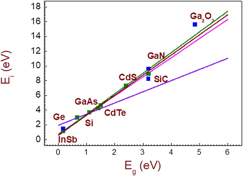
Applied Physics Letters ARTICLE scitation.org/journal/apl
where w(z) is the collection probability and h(z) is the depth depen- it is seen that if g is known, Ei can be obtained from the EBIC
dent excess carrier generation rate (generation function). As shown by measurements.
Donolato,9 the collection probability w(z), which is the current Values of g can be obtained by the Monte Carlo simulation, and
induced by a unit charge at a depth z, can be obtained as a solution of they are equal to 0.93, 0.905, 0.767, and 0.781 for Si, 4H–SiC, GaN,
the homogeneous diffusion equation with the corresponding bound- and Ga2O3, respectively. Of course, for the Schottky barriers, the
ary conditions. For thick semiconductor structures with a Schottky energy loss in metals should be taken into account, especially for the
barrier, the equation for w(z) can be written as case of thick metal and/or low beam energy; however, the losses can
@ 2 wðzÞ=@z 2 wðzÞ=L2 ¼ 0; (2) also be obtained by the Monte Carlo simulation of two-layer struc-
tures. Thus, if U is obtained from fitting Ic(Eb) dependences, Ei values
with the boundary conditions w(W) ¼ 1 at z ¼ 0 and w(z) ! 0 at can be easily calculated.
z ! 1, where L ¼ (Ds)0.5 is the excess carrier diffusion length, D is To check the method discussed, EBIC measurements were car-
the ambipolar diffusivity equal to the minority carrier diffusivity at ried out on standard Al-p-Si and Au-n-Si Schottky barriers. The
low excitation level, and s is the excess carrier lifetime. W is the deple- obtained Ei values varied in the range of 3.63–3.65 eV that correlates
tion region width. For L independent of z, w(z) ¼ exp[-(z-W)/L] for well with the literature value of 3.66 eV.16 For GaN, the difference
z > W and w(z) ¼ 1 for z W. For p-n junctions, the collection prob- between the calculated Ei value of 9.59 eV from the EBIC measure-
ability can be calculated using a similar diffusion equation with the ments and the reported value of 8.9 eV17 is about 7%. For 4H-Si, a
corresponding boundary conditions. comparison is less informative because the previously reported values
The generation function can be calculated by the Monte Carlo vary in the range from 5.0518 to 8.6 eV.19 Our approach gives the value
simulation. It should be stressed that, in such simulations, not only the Ei ¼ 8.23 eV for 4H–SiC.
backscattered energy but also the energy loss in the metal contact can For the prediction of Ei values in new materials, it can be useful
be taken into account. To simplify further calculations, the generation to have the empirical relation between the bandgap and the mean
function is usually approximated by the Gaussian function. For exam- electron–hole pair ionization energy. A few expressions for such a rela-
ple, for common semiconductor materials, it can be described as tion have been proposed.20–23 In Fig. 1, these dependences are shown
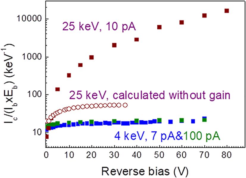
1:76 together with the experimental data from17,20 and the data obtained in
hðzÞ ¼ U exp 7:5ðz=R 0:3Þ2 (3) the present work. It is seen that the experimental data fit well with the
R
expressions from Refs. 20–22, with the best agreement of the experi-
for the case of Si.10 [U in Eq. (3) is the total generation rate of excess mental data to the expression20
carriers, R(nm) ¼ 17.1Eb(keV)1.75 is the electron range, and Eb is the
beam energy]. Ei ¼ 2:8Eg þ 0:6 eV: (8)
For GaN, the generation function can be described as11
As follows from Fig. 1, the Ei data obtained by the method used
" 2 #
3:207 z in the present letter correlate rather well with the experimental data
hðzÞ ¼ U exp A 0:11 ; (4) obtained for different materials and the empirical dependences. In par-
R R
ticular, for wide-bandgap materials, Eq. (8) seems to correctly predict
42:8; z < 0:11R the pair formation energy. This confirms the applicability of the
where R(nm) ¼ 13.2Eb(keV)1.75 and A ¼ . approach for measurements of the mean electron–hole pair creation
16:5; z 0:11R
For SiC, h(z) was obtained in Ref. 12 as energy. For the sake of convenience, it is generally agreed to present
the EBIC signal in the form of EBIC current Ic normalized by the
1:87
hðzÞ ¼ U exp 7:94ðz=R 0:28Þ2 ; (5)
R
where R(nm) ¼ 18.25Eb(keV)1.75.
For Ga2O3,13
" 2 #
1:603 z
hðzÞ ¼ exp A 0:22 ; (6)
R R
12:86; z < 0:22 R
where R(nm) ¼ 7.34Eb(keV)1.75 and A ¼ .
3:97; z 0:22 R
Fitting of the measured dependence of collected current on beam
energy with calculated ones allows not only to obtain the diffusion
length7,8 but also the total generation rate U in some structures W,14,15
which is equal to
E b Ib g
U¼ ; (7)
Ei FIG. 1. Experimental values of Ei from Refs. 17 and 20 (olive symbols) and
obtained in the preset work (blue symbols). Lines present the empirical expressions
where Eb and Ib are the beam energy and current, respectively, and g is from Ref. 20 (olive line), Ref. 21 (magenta line), Ref. 22 (wine line), and Ref. 23
the portion of beam energy deposited inside the semiconductor. Thus, (violet line).
Appl. Phys. Lett. 118, 202106 (2021); doi: 10.1063/5.0053301 118, 202106-2
Published under an exclusive license by AIP Publishing
Applied Physics Letters                                                                            ARTICLE              scitation.org/journal/apl

    product of Eb  Ib, Ic/(EbIb). Since at zero bias, the collected current
    for materials with low mobilities of one or both types of carriers (as is
    the case for Ga2O3 with low hole mobility) can be seriously affected by
    trapping at interface states, the normalized EBIC current is usually
    measured at high applied voltages to mitigate this trapping. This is
    done below for Ga2O3 Schottky diodes.
          We turn now to the measurements of Ei in b-Ga2O3. In the
    course of our previous and current work, we have looked at more than
    20 epitaxial films of b-Ga2O3 deposited by Halide Vapor Phase
    Epitaxy (HVPE) on bulk b-Ga2O3 substrates prepared by Edge-
    defined Film-fed Growth (EFG). The samples were acquired from
    Tamura/Novel Crystals Ltd. company in Japan, the main commercial
    manufacturer of high-quality b-Ga2O3 bulk and epitaxial material
    widely used to fabricate high-power devices based on b-Ga2O3.24,25 All
    these films were doped to n-type by Si and had net donor concentra-
                                                                                FIG. 2. Normalized collected current as a function of applied reverse bias for two
    tion between 1015 and 1017 cm3. The orientation of the films                Schottky diodes on b-Ga2O3 measured at Eb ¼ 4 keV.
    was (001), and the thickness was 10 lm. They were prepared on
    b-Ga2O3 substrates heavily doped with Sn to donor concentration of
    3  1018 cm3 cut from bulk crystals prepared by EFG. The Schottky          expression (8) describing the trends for many other semiconductors.
    diodes were made by e-beam evaporation of 20 nm of Ni. The back             (The corresponding value for Ga2O3 derived from the data in Fig. 2 is
    Ohmic contacts to the substrate side were made by e-beam evapora-           shown in Fig. 1.)
    tion of Ti/Au (20 nm/80 nm).4,5 Some of the samples were additionally             Unfortunately, the samples belonging to group I are in the
    subjected to irradiation with fast reactor neutrons,5 with 10 MeV or        minority among the Ga2O3 samples that we have measured. Only two
    20 MeV protons and 20 MeV a-particles,13,26–28 and some subjected to        samples showed such a behavior. In both cases, the Ei values were very
    treatment in dense Ar plasmas.29 EBIC measurements were performed           close to 15.6 eV. For the majority of the samples, the bias dependence
    as described in Refs. 4, 5, and 13. The samples were also characterized     of the normalized EBIC signal for low beam energies was quite strong,
    by current–voltage (I–V) measurements in the dark and under mono-           as shown for one of such group II samples by olive squares in Fig. 2.
    chromatic light illumination (wavelength range 259–940 nm), capaci-         These results were obtained for a sample with a net donor density of
    tance–voltage (C–V) profiling in the dark and under illumination (CV         5  1015 cm3 under excitation with the same low beam energy of
    or LCV profiling27,30), and by deep level transient spectroscopy with        4 keV creating charge carriers at a depth of 50 nm from the interface,
    electrical (DLTS) or optical (ODLTS) injection. Experimental details        while the SCR width at 0 V for the sample was 0.5 lm. Obviously,
    can be found in our earlier papers.4,5,13,26–29                             for this second group of samples, the EBIC data indicates the presence
          All EBIC measurement results fell into two unequal groups. For        of some multiplication mechanism resulting in the External Quantum
    group I, the normalized EBIC signal Ic/(Eb  Ib) was independent of         Efficiency (EQE) much higher than unity. The existence of this inter-
    the applied bias for beam energies such that they produced electron–        nal gain mechanism has been observed for as-grown HVPE films,4
    hole pairs well within the space charge region (SCR). This is the kind      films subjected to fast reactor neutron irradiation,5 HVPE epilayers
    of behavior observed for all previously studied semiconductor materi-       subjected to proton irradiation,26–28 or treatment in Ar plasmas.29 In
    als and predicted by Eqs. (1)–(7). It is simply the consequence of com-     all cases, we observed a similarly high gain in the photocurrent as in
    plete charge collection inside the SCR. Hence, once the energy              EBIC for Schottky diodes illuminated with above-bandgap light. (For
    deposited by the electron beam inside the SCR is calculated taking into     some as-grown samples, this has been demonstrated in Ref. 4; for neu-
    account the energy losses due to the absorption in the metal contact        tron irradiated samples, it was shown in Ref. 5; for proton irradiated
    and the backscattering of the incident electrons, the electron–hole         samples and Ar plasma treated samples, we have also recently shown
    energy formation Ei can be calculated using the measured value of the       this to be the case, and the actual results will be published separately).
    normalized EBIC signal and Eq. (7). Such dependence is presented in               The existence of gain mechanisms has been widely invoked to
    Fig. 2 for the beam energy 4 keV for one of the studied b-Ga2O3 sam-        explain the apparently high EQE of photocurrent in Ga2O3 and vari-
    ples that had net donor concentration 1.3  1016 cm3. As shown in          ously attributed to impact ionization,1–3 the operation of polaronic
    Ref. 5, under these conditions, the charge carriers are generated at the    Self-Trapped Hole (STH) states,31 or to trapping by deep hole traps.3–5
    depth lower than 50 nm, taking into account the energy absorption in        We can definitely rule out in our case the contribution of the impact
    the top Ni layer. The SCR width at 0 V was close to 0.3 lm.                 ionization simply because the electric field strength was very far from
    Experimental results are shown for this sample by solid blue squares.       the expected threshold of impact ionization near 5–8 MV/cm.32 The
    The data follows the behavior predicted by Eqs. (1)–(7). The initial        reasons we believe that the STH impact cannot be a major factor in
    slight increase in the signal with applied bias is most likely due to the   the observed phenomena at room temperature is that EBIC results
    charge collection loss near the interface with the Schottky diode metal     obtained for b-Ga2O3 Schottky diodes cannot be explained without
    because of the hole trapping by the surface states. For higher biases,      assuming that, at room temperature and above, holes in this material
    this effect is suppressed and the normalized EBIC signal vs bias            are mobile.4 As for the participation of deep hole traps, we have shown
    plateau observed can be used to extract the e-h formation energy from       in Refs. 4 and 5 that the amount of increase in EQE definitely corre-
    Eq. (7) as Ei ¼ 15.6 eV, close to the one predicted by the empirical        lates with the increased concentration of deep hole traps with an

Appl. Phys. Lett. 118, 202106 (2021); doi: 10.1063/5.0053301                                                                                          118, 202106-3
Published under an exclusive license by AIP Publishing
Applied Physics Letters                                                                                 ARTICLE            scitation.org/journal/apl

    optical ionization threshold near 2.3 eV and 3.1 eV, often attributed to           results of EBIC signal measurements as a function of bias for the group
    Ga vacancy acceptors, VGa, or VGa complexes with interstitial Ga,                  I sample from Fig. 2 when the beam energy is increased to 25 keV. In
    VGai.33,34 Recently, we have shown that such a correlation also holds              that case, the electron range will be close to 2.4 lm,13 so that up to
    for samples irradiated with 20 MeV protons or subjected to Ar plasma               25 V applied bias, a considerable part of the electron–hole pairs will
    treatment (the results are to be published separately). In all these cases,        be created outside the space charge region and collected due to the
    the holes trapped by the deep acceptors change the space charge den-               holes diffusion to the SCR boundary with the diffusion length close to
    sity in the part of the SCR, thus increasing the electric field strength            0.6 lm. Thus, for biases lower than 25 V, the collection efficiency will
    and decreasing the effective Schottky barrier height and enhancing the             be much lower than that observed in the case of Eb ¼ 4 keV,13 but the
    electron current flow through the diode.3,5 The photocurrent and                    contribution of the energy losses in the metal will be much lower than
    EBIC current then consists in Ga2O3 Schottky diodes of the “normal”                in the Eb ¼ 4 keV case. Hence, without the current “gain” term, the
    part common for all semiconductor materials and the “gain” part                    normalized EBIC signal should look as shown by the open diamonds
    Jdark[exp(DVbi/kBT) – 1],3 where Jdark is the dark current, kB is the              in Fig. 3. It can be seen, however, that the actual measurements go
    Boltzmann constant, T is the temperature, and DVbi is the change of                much higher than the calculated curve. This is because of the
    the Schottky barrier height due to trapping of holes on deep acceptors.            enhanced contribution of the “gain” term in EBIC current. Indeed, the
    In Ref. 5, we show that the change of the Schottky barrier height is               upper limit of the wo value in the DVbi expression above is increased
    closely related to the change in the density of deep traps Ndeep as                by about 50 times compared to the 4 keV case (2.4 lm vs 0.05 lm),
    DVbi ¼ qNdeepwo2/(2eeo), where q is the electronic charge, wo is the               which, for the same concentration of the deep acceptors, will produce
    thickness of the layer where the deep hole traps are recharged by light            an enormous increase in gain (these are only crude estimates not tak-
    or electron beam, e0 is the dielectric constant, and e is the relative per-        ing into account the diffusion of holes toward the Schottky diode).
    mittivity. The distinguishing feature of the group I samples that sepa-            Thus, even for group I samples, the estimated Ei value contains a small
    rate them from the group II samples with the high current gain is the              contribution from the “gain” term.
    much lower density of the deep acceptor hole traps with an optical                       Taking into account that any losses of collected current inside the
    threshold of 3.1 eV related to VGa and of traps with an optical thresh-            depletion region lead to the increase in the calculated Ei value, the
    old of 2.3 eV related to VGai. For the two samples in Fig. 2, LCV spec-            obtained value should be considered as the upper limit of Ei. Also,
    tra measurements27–30 give the concentration of the 2.3 eV VGai hole               the presence of even a small amount of deep hole traps could produce
    traps as 2  1014 cm3 for the sample from group I and 7  1014 cm3               some small error in the Ei estimate. This is because the presence of the
    for the sample from group II in which we also detected                             gain due to the hole trapping on deep acceptors will not be canceled
    2.5  1014 cm3 of the VGa acceptors.                                              out, even if Ei is determined from comparison with the signal from the
          Nevertheless, the concentration of the deep hole traps in the                well calibrated detectors, because in Schottky diodes, there still will be
    group I sample is not totally negligible and the current “gain” contri-            a contribution coming from the hole trapping and effective Schottky
    bution to EBIC is still present, albeit its magnitude is small for very            barrier decrease while in photoconductors this hole trapping will give
    low beam energies with very small thickness of the wo region where                 rise to additional enhancement of photocurrent because of the
    the traps can be recharged by the electron beam (the upper limit of wo             increased lifetime of electrons.
    is 50 nm for Eb ¼ 4 keV). The impact of these hole traps can, however,                   The reason why the concentration of deep traps can strongly
    become much more pronounced for higher beam energies recharging                    vary from sample to sample needs better understanding. The increase
    the hole traps in the thicker wo region. In Fig. 3, we compare the                 in the level of donor doping from 1016 cm3 to 1017 cm3 seems to
                                                                                       somewhat increase the concentration of deep acceptors,5 but the data
                                                                                       have been collected for very few samples with larger donor density.
                                                                                       [Most of the samples that we studied had net donor concentration
                                                                                       closer to (1–3)1016 cm3 often used for high-power rectifiers work.]
                                                                                       Since the deep acceptors responsible seem to be related to Ga vacancies
                                                                                       or their complexes, one would expect that changing the VI/III flows
                                                                                       ratio in HVPE should have a more pronounced effect than varying the
                                                                                       donor density in a rather narrow range, but no systematic studies of
                                                                                       that sort can be performed on commercially available samples. The Ei
                                                                                       measurements performed on the samples with the lowest possible
                                                                                       deep acceptors concentrations is at the moment the best we can do in
                                                                                       order to estimate the Ei value in b-Ga2O3. The Ei value obtained above
                                                                                       is about 10% larger than the 14.2 eV predicted by the expression (8).
                                                                                       The expressions proposed in Refs. 21 and 22 give values of 13.3 and
                                                                                       13.79 eV, respectively. There is some uncertainty in the value of the
                                                                                       bandgap of b-Ga2O3 that is differently quoted as ranging from 4.7 eV
     FIG. 3. Normalized collected current as a function of applied reverse bias mea-   to 4.9 eV.
     sured at the beam energy of 4 keV with the beam current of 7 pA (blue squares)
                                                                                             Nevertheless, our estimated value differs from the smallest value
     and 100 pA (olive squares) and at the beam energy of 25 keV and beam current
     10 pA (solid wine squares); also shown is the calculated bias dependence of the   of 13.3 eV by 15% only. Taking into account that the state-of-the-art
     normalized EBIC signal without taking into account the current gain term (open    b-Ga2O3 Schottky diodes due to reasons discussed above do not allow
     diamonds).                                                                        to obtain the Ei value more precisely, and the value obtained in the

Appl. Phys. Lett. 118, 202106 (2021); doi: 10.1063/5.0053301                                                                                         118, 202106-4
Published under an exclusive license by AIP Publishing
Applied Physics Letters ARTICLE scitation.org/journal/apl
13
present work from the EBIC measurements or those calculated using E. B. Yakimov, A. Y. Polyakov, N. B. Smirnov, I. V. Shchemerov, J. Yang, F.
the empirical expressions from20–22 can be used for the mean electron– Ren, G. Yang, J. Kim, and S. J. Pearton, “Diffusion length of non-equilibrium
minority charge carriers in b-Ga2O3 measured by electron beam induced
hole pair creation energy in b-Ga2O3 for the prediction of charged par-
current,” J. Appl. Phys. 123, 185704 (2018).
ticle detector parameters and other cases where the knowledge of Ei 14
E. B. Yakimov, P. S. Vergeles, A. Y. Polyakov, N. B. Smirnov, A. V. Govorkov,
value is necessary. I.-H. Lee, C. R. Lee, and S. J. Pearton, “Spatial variations of doping and lifetime
To conclude, the electron–hole pair formation in Ga2O3 indeed in epitaxial laterally overgrown GaN,” Appl. Phys. Lett. 90, 152114 (2007).
15
can be reasonably accurately determined by fitting the normalized E. B. Yakimov, P. S. Vergeles, A. Y. Polyakov, N. B. Smirnov, A. V. Govorkov,
EBIC signal collection efficiency, but these measurements have to be I.-H. Lee, C. R. Lee, and S. J. Pearton, “Donor nonuniformity in undoped and
Si doped n-GaN prepared by epitaxial lateral overgrowth,” Appl. Phys. Lett. 92,
performed at low beam energies when the excitation depth is much 042118 (2008).
lower than the space charge region width. In addition, it is important 16
F. Scholze, H. Rabus, and G. Ulm, “Mean energy required to produce an
to check the independence of the collected current on bias and that the electron-hole pair in silicon for photons of energies between 50 and 1500 eV,”
density of deep hole traps is low to avoid photoconductive gain effects. J. Appl. Phys. 84, 2926 (1998).
17
J. D. Wrbanek, S. Y. Wrbanek, G. C. Fralick, and L. Y. Chen, “Micro-fabricated
solid state radiation detectors for active personal dosimetry,” Report No.
The work at NUST MISiS was supported in part by Grant No. NASA/TM 214674 (NASA, 2007).
K2-2020-040 under the Program to increase Competitiveness of 18
M. V. S. Chandrashekhar, C. I. Thomas, and M. G. Spencer, “Measurement of
NUST MISiS among the World Leading Scientific and Educational the mean electron-hole pair ionization energy in 4H SiC,” Appl. Phys. Lett. 89,
centers (Program funded by the Russian Ministry of Science and 042113 (2006).
19
Education). The work at IMT RAS was supported in part by the A. A. Lebedev, A. M. Ivanov, and N. B. Strokan, “Radiation resistance of SiC
and nuclear-radiation detectors based on SiC films,” Semiconductors 38, 125
State Task No. 075-00920-20-00.
(2004).
The work at UF was sponsored by Department of the Defense, 20
C. A. Klein, “Bandgap dependence and related features of radiation ionization
Defense Threat Reduction Agency, part of Interaction of Ionizing energies in semiconductors,” J. Appl. Phys. 39, 2029 (1968).
21
Radiation with Matter University Research Alliance (IIRM-URA) T. Kobayashi, “Average energy to form electron-hole pairs in GaP diodes with
under Award No. HDTRA1-20-2-0002 (Jacob Calkins) and also by alpha particles,” Appl. Phys. Lett. 21, 150 (1972).
22
NSF DMR No. 1856662 (James Edgar). R. C. Alig and S. Bloom, “Electron-hole-pair creation energies in semi-
conductors,” Phys. Rev. Lett. 35, 1522 (1975).
23
DATA AVAILABILITY S. Butera, G. Lioliou, A. B. Krysa, and A. M. Barnett, “Measurement of the
electron–hole pair creation energy in Al0.52In0.48P using x-ray radiation,” Nucl.
The data that support the findings of this study are available Instrum. Methods Phys. Res., Sect. A 879, 64 (2018).
within this article. 24
See www.tamura-ss.co.jp/en/products for a listing of available substrate and epi
films of gallium oxide.
25
REFERENCES S. J. Pearton, J. Yang, P. H. Cary, F. Ren, J. Kim, M. J. Tadjer, and M. A.
1
Mastro, “A review of Ga2O3 materials, processing and devices,” Appl. Phys.
O. Katz, V. Garber, B. Meyler, G. Bahir, and J. Salzman, “Gain mechanism in Rev. 5, 011301 (2018).
GaN Schottky ultraviolet detectors,” Appl. Phys. Lett. 79, 1417 (2001). 26
A. Y. Polyakov, N. B. Smirnov, I. V. Shchemerov, E. B. Yakimov, J. Yang, F.
2
J. Xu, W. Zheng, and F. Huang, “Gallium oxide solar-blind ultraviolet photode- Ren, G. Yang, J. Kim, A. Kuramata, and S. J. Pearton, “Effect of 10 MeV proton
tectors: A review,” J. Mater. Chem. C 7, 8753 (2019). irradiation on electrical properties and recombination in Ga2O3 Schottky
3
X. Chen, F.-F. Ren, J. Ye, and S. Gu, “Gallium oxide-based solar-blind ultravio- diodes,” Appl. Phys. Lett. 112(3), 032107 (2018).
let photodetectors,” Semicond. Sci. Technol. 35, 023001 (2020). 27
A. Y. Polyakov, N. B. Smirnov, I. V. Shchemerov, E. B. Yakimov, S. J. Pearton, C.
4
E. B. Yakimov, A. Y. Polyakov, N. B. Smirnov, I. V. Shchemerov, P. S. Fares, J. Yang, F. Ren, J. Kim, P. B. Lagov, V. S. Stolbunov, and A. Kochkova,
Vergeles, E. E. Yakimov, A. V. Chernykh, M. Xian, F. Ren, and S. J. Pearton, “Defects responsible for charge carrier removal and correlation with deep level
“Role of hole trapping by deep acceptors in electron-beam-induced current introduction in irradiated b-Ga2O,” Appl. Phys. Lett. 113, 092102 (2018).
measurements in b-Ga2O3 vertical rectifiers,” J. Phys. D: Appl. Phys. 53, 28
A. Y. Polyakov, N. B. Smirnov, I. V. Shchemerov, S. J. Pearton, F. Ren, A. V.
495108 (2020). Chernykh, P. B. Lagov, and T. V. Kulevoy, “Hole traps and persistent photoca-
5
E. B. Yakimov, A. Y. Polyakov, I. V. Shchemerov, N. B. Smirnov, A. A. Vasilev, pacitance in proton irradiated Ga2O3 films doped with Si,” APL Mater. 6,
P. S. Vergeles, E. E. Yakimov, A. V. Chernykh, A. S. Shikoh, F. Ren, and S. J. 096102 (2018).
Pearton, “Photosensitivity of Ga2O3 Schottky diodes: Effects of deep acceptor 29
A. Y. Polyakov, I.-H. Lee, N. B. Smirnov, E. B. Yakimov, I. V. Shchemerov, A.
traps present before and after neutron irradiation,” APL Mater. 8, 111105 V. Chernykh, A. I. Kochkova, A. A. Vasilev, P. H. Carey, F. Ren, D. J. Smith,
(2020). and S. J. Pearton, “Defects at the surface of b-Ga2O3 produced by Ar plasma
6
D. B. Wittry and D. F. Kyser, “Cathodoluminescence at p-n Junctions in exposure,” APL Mater. 7, 061102 (2019).
GaAs,” J. Appl. Phys. 36, 1387 (1965). 30
A. M. Armstrong, M. H. Crawford, A. Jayawardena, A. Ahyi, and S. Dhar,
7
E. B. Yakimov, “What is the real value of diffusion length in GaN?,” J. Alloys “Role of self-trapped holes in the photoconductive gain of b-Ga2O3 Schottky
Compd. 627, 344 (2015). diodes,” Appl. Phys. 119, 103102 (2016).
8 31
E. B. Yakimov, “Diffusion length measurements in GaN,” Jpn. J. Appl. Phys., Z. Zhang, E. Farzana, A. R. Arehart, and S. A. Ringel, “Deep level defects
Part 1 55, 05FH04 (2016). throughout the bandgap of (010) b-Ga2O3 detected by optically and thermally
9
C. Donolato, “A reciprocity theorem for charge collection,” Appl. Phys. Lett. stimulated defect spectroscopy,” Appl. Phys. Lett. 108, 052105 (2016).
32
46, 270 (1985). S. J. Pearton, F. Ren, M. Tadjer, and J. Kim, “Perspective: Ga2O3 for ultra-high
10
H. J. Fitting, H. Glaefeke, and W. Wild, “Electron Penetration and Energy power rectifiers and MOSFETS,” J. Appl. Phys. 124, 220901 (2018).
33
Transfer in Solid Targets,” Phys. Status Solidi A 43, 185 (1977). M. E. Ingebrigtsen, A. Y. Kuznetsov, B. G. Svensson, G. Alfieri, A. Mihaila, U.
11
E. B. Yakimov, S. S. Borisov, and S. I. Zaitsev, “EBIC measurements of small dif- Badstubner, A. Perron, L. Vines, and J. B. Varley, “Impact of proton irradiation on
fusion length in semiconductor structures,” Semiconductors 41, 411 (2007). conductivity and deep level defects in b-Ga2O3,” APL Mater. 7, 022510 (2019).
12 34
A. A. Svintsov, A. A. Krasnov, M. A. Polikarpov, A. Y. Polyakov, and E. B. A. Karjalainen, V. Prozheeva, K. Simula, I. Makkonen, V. Callewaert, J. B. Varley,
Yakimov, “Betavoltaic battery performance: Comparison of modeling and and F. Tuomisto, “Split Ga vacancies and the unusually strong anisotropy of
experiment,” Appl. Radiat. Isot. 137, 184 (2018). positron annihilation spectra in b-Ga2O3,” Phys. Rev. B 102, 195207 (2020).
Appl. Phys. Lett. 118, 202106 (2021); doi: 10.1063/5.0053301 118, 202106-5
Published under an exclusive license by AIP PublishingYou can also read