Extreme Ultraviolet Lithography
←
→
Page content transcription
If your browser does not render page correctly, please read the page content below
4                                                                                               S&TR November 1999

                                           Extreme
                                           Ultraviolet
                                           Lithography
                                                                   Imaging the Future

    Livermore researchers
    are part of a collaboration
                                           T    WENTY-FIVE years ago, the computing equivalent of today’s
                                                laptop was a room full of computer hardware and a cartload of
                                           punch cards.
                                               Since then, computers have become much more compact and
                                           increasingly powerful largely because of lithography, a basically
    between private industry               photographic process that allows more and more features to be crammed
                                           onto a computer chip. Light is directed onto a mask—a sort of stencil
    and DOE laboratories                   of an integrated circuit pattern—and the image of that pattern is then
                                           projected onto a semiconductor wafer covered with light-sensitive
                                           photoresist. Creating circuits with smaller and smaller features has
    dedicated to making extreme            required using shorter and shorter wavelengths of light.
                                               However, current lithography techniques have been pushed just
    ultraviolet lithography                about as far as they can go. They use light in the deep ultraviolet range—
                                           at about 248-nanometer wavelengths—to print 150- to 120-nanometer-
                                           size features on a chip. (A nanometer is a billionth of a meter.) In the
    the technology of choice               next half dozen years, manufacturers plan to make chips with features
                                           measuring from 100 to 70 nanometers, using deep ultraviolet light of
    for manufacturing the                  193- and 157-nanometer wavelengths. Beyond that point, smaller
                                           features require wavelengths in the extreme ultraviolet (EUV) range.
                                           Light at these wavelengths is absorbed instead of transmitted by
    next generation of                     conventional lenses. The result: no light, no image, no circuit.
                                               Semiconductor manufacturers are, therefore, at a critical juncture. Soon,
    microcomputer chips.                   they must decide which lithographic horse to back in the race to the next

                               Lawrence Livermore National Laboratory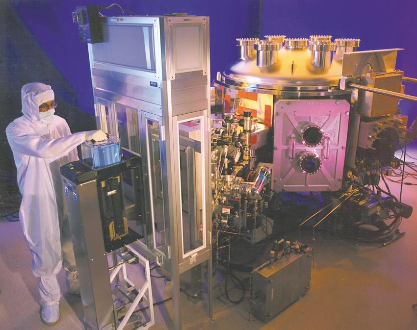
S&TR November 1999                                                                                                     EUVL Progress Report        5

generation of microchip manufacturing.        The resulting microprocessors would be              says Don Sweeney, Lawrence
There are currently four possible             a hundred times more powerful than                  Livermore’s program manager for
alternatives: EUV, x-ray, electron-           those made today. Memory chips would                EUVL. “To put this technology into
beam, and ion-beam lithography.               be able to store a thousand times more              production facilities in 10 years, we need
                                              information than at present.                        to show that the technology can work
Creating a Virtual Laboratory                    “Lithography is generally viewed as              under real manufacturing conditions.”
    Two years ago, three Department           the enabling technology for each new                   The VNL’s current focus is on
of Energy national laboratories—              generation of semiconductor devices,”               building and integrating the necessary
Lawrence Livermore, Lawrence
Berkeley, and Sandia/California—
formed the Virtual National Laboratory
(VNL) to research and develop extreme                                             What’s at Stake
ultraviolet lithography (EUVL)
technology. The VNL is funded by the                        . . . [T]he first 30 years of the integrated circuit had from two to five
                                                        times the impact on the U.S. economy as the first 30 years of the
Extreme Ultraviolet Limited Liability                   railroad. Or, to put it another way, the transformation of the nineteenth
Company—a consortium of Intel                           century U.S. economy by the railroad took 60 years to achieve half the
Corporation, Motorola Corporation,                      effect that microelectronics had over 30 years.
Advanced Micro Devices Corporation,                                                                                —Kenneth Flamm
and Micron Technology, Incorporated—                                          “More for Less: The Economic Impact of Semiconductors”
                                                                                                                      December 1997
in one of the largest cooperative research
and development agreements within                   Semiconductors are ubiquitous in our lives. They are found in our cars, televisions, radios,
the Department of Energy. The three-            telephones, stereos, personal computers, children’s toys—even dishwashers and ovens.
year, $250-million venture is dedicated         According to research conducted by the Semiconductor Industry Association and the World
to developing the EUVL technology               Bank, each person worldwide uses on the average about ten million transistors in a lifetime,
for commercial manufacturing of                 with this consumption increasing 55 percent each year. By the year 2008, projections are
computer chips and to move this                 that each person will consume a billion transistors.
technology into production facilities               It’s no wonder then that the annual sale of semiconductors worldwide will soon reach
                                                about one trillion dollars—the equivalent of the gross national product of the United
in the first decade of the 21st century.
                                                States. Furthermore, it’s no wonder that the next generation of
    Each national laboratory brings             lithographic technology—which is seen as
unique contributions to this effort.            the “gating technology” to the next
Lawrence Livermore supplies its                 generation of integrated circuits—
expertise in optics, precision                  is of such great interest to
engineering, and multilayer coatings.           semiconductor manufacturers
Sandia provides systems engineering,            throughout the world.
the photoactive polymer thin film
exposed by the light, and the light source.
Berkeley contributes its Advanced
Light Source capability to generate
EUV light to characterize optics and
resists at the nanometer scale.
    The VNL’s lithography system
uses mirrors to project the image of a
reflective mask onto the photoresist-
coated semiconductor wafer. Ultimately,
this system will enable a microchip to be
manufactured with etched circuit lines
smaller than 100 nanometers in width,
extendable to below 30 nanometers.

                                              Lawrence Livermore National Laboratory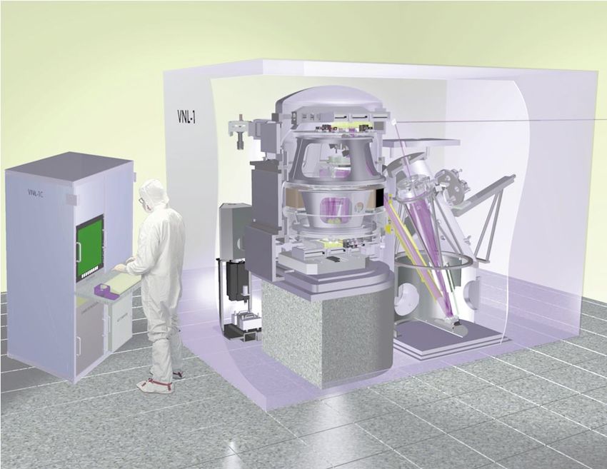
6 EUVL Progress Report S&TR November 1999
Using a prototype system, technologies into an engineering test
the Virtual National stand (ETS). Each national laboratory
Photo courtesy of Sandia National Laboratories/California.
Laboratory has successfully spearheads specific development areas
printed lines as small as for the ETS and for the systems beyond.
50 nanometers (billionths Lawrence Livermore is leading the
of a meter) wide in efforts to develop the optical systems
photoresist. Current and components, thin films, masks,
lithographic tools used in and submicrometer metrology required
the semiconductor industry for EUVL.
print patterns with
180-nanometer-size Brighter Light Is Key
features. The ETS (see the box on p. 7)
includes a condenser optics box and
a projection optics box. Both boxes
house complex optical trains of
precision concave and convex
aspherical mirrors.
The main role of the condenser
optics box is to bring light to the
Mask stage reflective pattern on the mask. “We
want to bring as much light to the mask
and, ultimately, the wafer, as possible,”
explains Sweeney. “The more light we
deliver, the shorter the exposure time.
It’s like taking a picture with a camera.
A picture taken in bright noonday sun
requires a shorter exposure time than
does a picture of the same scene taken
Projection
optics
at twilight.”
For the semiconductor industry,
brighter EUV images mean shorter
exposure times, which translate to
manufacturing more chips at a faster rate.
The optics design team from Lawrence
Plasma Livermore and Sandia designed a
source Condenser
optics condenser optics system that collects
Wafer stage and transports a significant fraction of
the EUV light from the source to the
reflective mask.
Once the image is reflected from the
mask, it travels through the projection
optics system. According to Sweeney, the
projection optics box is the optical heart
The optical layout of the engineering test stand for extreme ultraviolet of the lithographic exposure system. “It is
(EUV) lithography. The EUV radiation is produced at the plasma source, to the system what an engine is to a car,”
transmitted through the condenser optics to the mask, reflected from the he explains. The four mirrors of the ETS
mask onto the four mirrors of the projection optics box, and delivered to the projection optics system reduce the
EUV-sensitive film on the semiconductor wafer. Each mirror in the system has image and form it onto the wafer.
81 layers of reflective coatings that must be applied with extreme precision. At “Again, imagine using a pocket camera.
the short wavelengths used in the process, the total thickness of each mirror’s The camera lens transmits an image to
coatings must deviate less than an atom if the mask pattern is to be reflected the film, which—like the wafer—has a
without distortion. One such mirror is shown on p. 4. light-sensitive surface,” says Sweeney.
Lawrence Livermore National Laboratory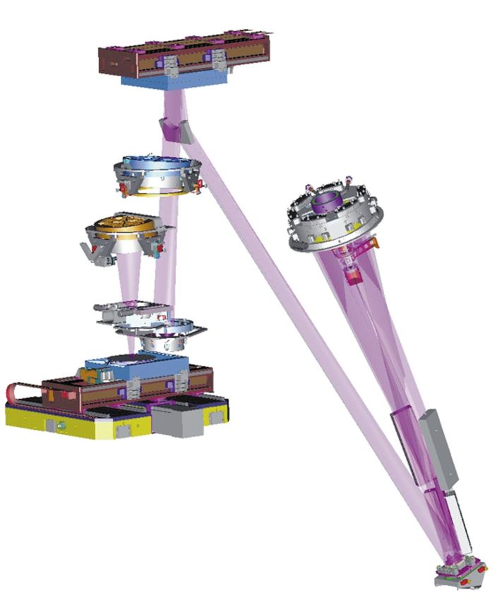
S&TR November 1999                                                                                                 EUVL Progress Report       7

    The optics teams are now working         can be used to coat mirrors as large as
on advanced designs for the projection       40 centimeters in diameter.
optics. They have a six-mirror design that
promises to extend EUVL systems so           The Mask-Making Challenge
that they can print features as small as        Industry experts generally agree
30 nanometers— a significant jump from       that the biggest challenges and risks
the 70-nanometer limit of the ETS.           for the next generation of lithography
    According to Sweeney, extendability      systems involve the mask—that is, the
to smaller features is an important          master pattern used to “print” the
requirement for whatever lithographic        semiconductor circuits onto the silicon
technology the semiconductor industry        wafers or chips. The technology that
finally decides to back.                     successfully overcomes the hurdles of
                                             mask production has a good chance of
Applying Uniform Thin Films                  becoming the preferred choice.
    Part of the success of the EUVL             In EUVL, a mask is produced by
technology is due to the immense strides     applying multilayers of molybdenum
                                                                                                The extreme ultraviolet lithography
Lawrence Livermore has made in               and silicon to a flat substrate. The circuit
                                                                                                projection optics system in final assembly.
producing the highly reflective              pattern is produced by applying a final
multilayers that are used on the ETS’s
optical mirrors as well as on the mask.
    The projection and condenser
optical systems require mirrors that                The Engineering Test Stand Provides a Prototype
reflect as much EUV light as possible.
Manufacturing these mirrors has been               The Virtual National Laboratory is developing, designing, and building a prototype
a challenge because, in addition to            extreme ultraviolet lithography (EUVL) system called the engineering test stand (ETS) at
being highly reflective, they must have        Sandia National Laboratories/California. The ETS uses laser-produced plasmas to supply
surface coatings that are essentially          the extreme ultraviolet radiation needed. The radiation travels through a complex
perfectly uniform.                             condenser optics system before reflecting from a lithographic mask. That image is then
    Lawrence Livermore and Lawrence            projected by the projection optics onto a semiconductor wafer.
Berkeley developed advanced multilayer             “The basic building blocks are the same as those found in systems operating at visible
                                               wavelengths, except their forms are different, because of the short wavelength of EUV,”
coatings of molybdenum and silicon that
                                               says Don Sweeney, Lawrence Livermore’s program leader for EUVL.
can reflect nearly 70 percent of the EUV           Because all materials, including nitrogen and oxygen, absorb EUV, the machine must
light at a wavelength of 13.4 nanometers.      operate in a vacuum and use reflective mirrors and masks. The ETS has six essential
Applying these coatings evenly is a            subsystems: a laser-produced plasma EUV source, condenser optics, projection optics,
difficult task even when a mirror is flat,     a mask, precision scanning stages, and a vacuum enclosure.
but EUVL mirrors are either convex or
concave. Any small nonuniformity in                                                                                  A conceptual
the coatings destroys the shape of the                                                                               drawing of the
optics and results in distorted patterns                                                                             extreme ultraviolet
printed on the chips.                                                                                                engineering test
    In the past year, the development                                                                                stand. The goal of
of a new precision deposition system                                                                                 the ETS is to
provided a major advance in applying                                                                                 demonstrate how
these thin films to optics. (See S&TR,                                                                               ultraviolet
October 1999, p. 12.) This system,                                                                                   wavelengths can
which won a 1999 R&D 100 Award,                                                                                      be used to print
is so precise that 81 layers of                                                                                      patterns on
molybdenum and silicon, each about                                                                                   integrated circuits
3.5 nanometers thick, can be deposited                                                                               at production levels
over a 150-millimeter area so that the                                                                               and sizes.
total thickness over the surface deviates
by less than an atom. The technique

                                             Lawrence Livermore National Laboratory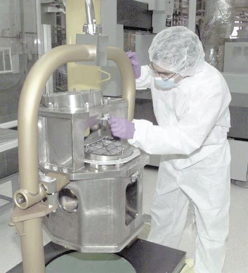
8   EUVL Progress Report                                                                                       S&TR November 1999

    EUV-absorbing metal layer and then          ultimate goal for the system is to add        The question becomes, what is this
    etching away the metal to form the          no more than 0.001 defects per square         critical size? “We’ve been modeling for
    image of the circuit.                       centimeter to the finished wafer blank.       a long time to see how different sizes
       One key requirement is to produce a         The system has also been upgraded to       and kinds of defects affect the final
    mask with essentially no defects. Any       process 200-millimeter wafers—the size        product,” says Scott Burkhart, group
    small defect ends up being replicated, or   used in industry—up from 150-millimeter       leader for mask blank development.
    printed, in the lithography process onto    wafers. The ability to process larger         “We finally conducted experiments
    the computer chips being manufactured,      wafers for mask substrates means both         that are setting the lower bound of
    thus damaging the chips’ complex            that the technology is working with           critical defect size.”
    circuitry. A key breakthrough in this       industry standards and that patterns for          The group has also made strides in
    area was the development of an Ultra        larger chips can be placed on the wafer.      repair strategies for mask defects.
    Clean Ion Beam Sputter Deposition              The Lawrence Livermore team has            “One mask can cost tens of thousands
    System about two years ago. This            also conducted groundbreaking                 of dollars,” notes Burkhart. “When
    system—also an R&D 100 Award                experiments looking at the propagation        possible, repairing the defects saves
    winner—produces precise, uniform,           of defects during multilayer film growth.     the industry a lot of money.”
    highly reflective masks with fewer          All masks have defects of some kind—
    defects than those produced by              some more, some less. First of all, there     Measuring at the Atomic Level
    conventional physical deposition            are defects that arrive on the wafer             Until recently, it was impossible to
    processes. (See S&TR, October 1997,         from the manufacturer. These are              accurately measure a mirror surface
    p. 8.) In April 1999, the team made         analogous to the pinholes and dust one        for high and low spots of a few atoms.
    significant improvements to the system’s    finds on photographic negatives. Defects      An R&D 100 Award–winning
    sputtering shield design and other          smaller than a certain critical size are      interferometer developed at the
    operational parameters. The system          covered up by the film layers and present     Laboratory two years ago—called the
    now consistently produces fewer than        no problem. However, defects larger           phase-shifting diffraction interferometer
    0.1 defects per square centimeter—          than this critical size persist through the   (PSDI)—changed all that. (See S&TR,
    a factor-of-8 improvement over defect       coating process and must be repaired or       October 1997, p. 6.)
    densities produced in 1998.                 reckoned with in some way.                       Like all interferometers, the PSDI
       In fact, under the best operating           There are also defects created by the      uses the interference pattern of two
    conditions, the system adds as few as       coating process itself: a few atoms too       waves of light to measure objects or
    0.04 median defects per square centimeter   many in any one area can create a bump        phenomena. These light waves are
    during a coating run of 25 wafers. The      that will affect the final circuit pattern.   usually imperfect because of the

    The Ultra Clean Ion Beam
    Sputter Deposition System,
    developed at Lawrence
    Livermore, is used to produce
    precise, uniform, highly
    reflective masks. A key
    requirement of the next-
    generation lithography system
    is that it produce virtually
    defect-free masks. The
    system contributes fewer
    than 0.1 defects per square
    centimeter to each mask.
    The ultimate goal for extreme
    ultraviolet lithography is to add
    no more than 0.001 defects per
    square centimeter to a finished
    wafer blank.

                                                Lawrence Livermore National Laboratory
S&TR November 1999                                                                                                     EUVL Progress Report           9

                                                                       Spherical
imperfect condition of the surface or                                 measurement                         Spherical
lens from which they emanate. Any                                      wavefront                          reference
imperfection introduces error into the                                 from fiber    Optical              wavefront                Single-mode
                                                      Single-mode                    system               from fiber
measurements. The PSDI produces a                                                                                                  optical fiber
                                                      optical fiber                 under test
nearly perfect spherical wavefront using
diffraction. In diffraction, light passes     Fiber
                                               core
around an object or through a hole,
                                                                                              Aberrant                         Semitransparent
breaking up in the process. In the PSDI,
                                                                                              wavefront                          metallic film
two light beams pass through two
separate optical fibers. When light exits
the surface of each fiber, it diffracts,                                                 Aberrant
forming nearly perfect spherical                                                        wavefront
                                                                                      reflected from
wavefronts. Because the two wavefronts                    Interference                   fiber face
are generated independently, their                           pattern
relative amplitude and phase can be
controlled, providing contrast adjustment     Schematic of the phase-shifting diffraction interferometer which uses two single-mode optical fibers.
and phase-shifting capability for the         In this example, the interferometer is testing a lens, but the setup is similar for testing mirrors.
highest possible accuracy.
    The measurement wavefront passes
through the optical system being tested,      funded organization of semiconductor               Key Words: Extreme Ultraviolet Limited
which induces aberrations in the              manufacturers.                                     Liability Company, extreme ultraviolet
wavefront and causes it to focus on the           At its annual meeting, International           lithography (EUVL), masks, phase-
                                                                                                 shifting diffraction interferometer
endface of the other fiber. Here, the         Sematech evaluated the four next-
                                                                                                 (PSDI), precision deposition system,
wavefront reflects off a semitransparent      generation lithographic technologies—              reflective multilayers, submicrometer
metallic film of the fiber end’s surface      EUV, x-ray, electron-beam, and ion-                metrology, thin films, Ultra Clean Ion
and interferes with the reference             beam—and strongly recommended                      Beam Sputter Deposition System, Virtual
wavefront to generate an interference         EUV lithography. “Their                            National Laboratory (VNL).
pattern. The pattern is then recorded         recommendation gave our efforts
by a charge-coupled-device camera.            important momentum,” notes Sweeney.                For further information contact
    Over the past three years, many           “It validated what we already knew:                Donald Sweeney (925) 422-5877
                                                                                                 (sweeney4@llnl.gov). Or visit the
EUV optics have been measured using           that we have a winning combination in
                                                                                                 Lawrence Livermore EUV lithography
this interferometer, including both           the three national laboratories and our            Web site at http://lasers.llnl.gov/
concave and convex spherical and              industrial partners and that our strength          lasers/IST/euvl.html.
aspherical mirrors and completed              comes from working together.”
projection systems. The PSDI is now a                                      —Ann Parker
reliable production tool for measuring
the overall surface shape of those
aspherical optics that have a specification     About the Scientist
of 0.50 nanometers or less and has
successfully measured errors in the
surface shape down to 0.35 nanometers.                          DONALD SWEENEY received his B.S., M.S., and Ph.D in
The Livermore metrology team is                                 mechanical engineering from the University of Michigan at Ann
upgrading the system so that it can                             Arbor in 1968, 1969, and 1972, respectively. He was a professor
be used to measure errors in the                                at Purdue University from 1972 to 1983, after which he became a
overall surface shape as small as                               department manager at Sandia National Laboratories/California and
0.15 nanometers.                                                assumed responsibility for a research program in optical diagnostics.
                                                                   Sweeney joined Lawrence Livermore’s Advanced
EUV Pulling Ahead in the Race                 Microtechnology Program (AMP) in early 1993 and soon became deputy program
   Last December, the VNL’s work              leader for Optics Technology. In February 1999, AMP reorganized and became the
paid off with a vote of confidence from       Information Science and Technology Program, where he is currently deputy program
International Sematech, a privately           leader for Extreme Ultraviolet Lithography and Advanced Optics.

                                              Lawrence Livermore National Laboratory
You can also read