Firefly E1608 and Firefly E2218 - Details on handling and processing
←
→
Page content transcription
If your browser does not render page correctly, please read the page content below
www.osram-os.com

Application Note No. AN088

Firefly® E1608 and Firefly® E2218 — Details on handling
and processing

Application Note
                                               Valid for:
                                               Firefly® E1608
                                               Firefly® E2218

Abstract
For wearable applications like fitness tracking, health
monitoring or similar OSRAM Opto Semiconductors offers
especially small and compact top emitter as the Firefly® E1608
and Firefly® E2218.
The following application note provides a short product
introduction followed by handling and processing information
for an appropriate implementation of the LED.
For more information on health monitoring applications and
appropriate products, please refer to the application note
“AN147_Health monitoring”.

           Further information:
           AN147_Health monitoring
           AN036_Processing of SMD LED

                                                            Author: Retsch Stefanie / Lex, Florian

2020-01-31 | Document No.: AN088                                                            1/9
www.osram-os.com
Table of contents
A. Basic information ....................................................................................................2
B. Handling and assembly information .......................................................................3
ESD stability ........................................................................................................3
Pick and place ....................................................................................................3
Solder pad design ...............................................................................................4
Assembly process ..............................................................................................5
Solder quality ......................................................................................................6
Cleaning ..............................................................................................................8
Storage ...............................................................................................................8
A. Basic information
Wearable applications can be realized with integrated solutions (emitters and
detectors integrated in a single package) or through discrete components (single
LEDs and photo-detectors). For both variations OSRAM Opto Semiconductors
offers suitable products.
A system setup with discrete components offers more design freedom.
Depending on the system requirements, various geometries can be selected and
different components can be combined. For these application cases, the use of
the Firefly® E1608 or Firefly® 2218 as emitters are the right choice. (Table 1
provides an product overview.)
Due to its compact size the Firefly® E1608 enables flexible product designs. It
allows to combine different wavelengths and typical brightness levels, all
matching the application.
For highest system efficiency a more efficient chip in a larger package design is
used at the Firefly® 2218. This enables a long battery life in wearable
applications.
2020-01-31 | Document No.: AN088 2/9www.osram-os.com
Table 1: Product overview
Firefly® E1608 Firefly® 2218
Properties Compact package size Highest system efficiency
Enables flexible product designs More efficient chip
Package Size 1.6 x 0.6 x 0.8 mm³ 2.2 x 1.8 x 0.6 mm³
ESD stability 2 kV “Class 2 HBM” 8 kV “Class 3B HBM”
For more information on health monitoring application, suitable photo-detectors
and system setup recommendations, please refer to the application note “Health
monitoring”.
B. Handling and assembly information
The Firefly® E1608 and the Firefly® E2218 have been designed to be very robust
packages. The following part provides handling and assembly information. As is
the case for all LEDs from OSRAM Opto Semiconductors, the LEDs also fulfills
the current RoHS guidelines (European Union and China) and therefore contains
no lead or other defined hazardous substances.
ESD stability
Firefly® E1608. Although there is no additional ESD protection included, the
LED provides ESD stability of up to 2 kV. It is assigned to the “Class 2 HBM”
category in accordance with ANSI / ESDA / JEDEC JS-001. With this class the
Firefly® E1608 can be considered as uncritical for processing and assembly by
state of the art SMT equipment aligned with ESD precautions. To achieve higher
ESD protection on the system level, additional ESD protection must be applied.
Firefly® E2218. As an additional ESD protection is included the LED provides
ESD stability of up to 8 kV. It is assigned to the “Class 3B HBM” category in
accordance with ANSI / ESDA / JEDEC JS-001. With this class the
Firefly® E2218 can be considered as uncritical for processing and assembly by
state of the art SMT equipment aligned with ESD precautions. To achieve higher
ESD protection on the system level, additional ESD protection must be applied.
Pick and place
Although manual handling and assembly is possible, automatic placement is
recommended.
An automatic assembly process is recommended. Figure 1 shows
recommended nozzles for automated placement machines.
2020-01-31 | Document No.: AN088 3/9www.osram-os.com
Figure 1: Recommended SIPLACE nozzle
Firefly® E1608 Firefly® E 2218
2.2
1.7
14
1.1
1.6
0,9 1,5
SIPLACE nozzle 911 SIPLACE nozzle 713 / 913
Manual handling Firefly® E1608. Special care must be taken if the
Firefly® E1608 is handled manually. The LED must not be lifted from the top,
because high forces can cause damage to the surface. In addition, it is
recommended to hold the LED package as shown in Figure 2 by using a tweezer
and applying the force equally to the entire LED package.
Manual handling Firefly® E2218. In contrast to the Firefly® E1608, the
Firefly® E2218 must not be taken by using a tweezer. If manual handling is
necessary only vacuum tweezers are recommended like shown in Figure 2.
Figure 2: Recommended manual handling
Firefly® E1608 Firefly® E 2218
Solder pad design
PCBs not only serve as a mechanical substrate and electrical contacting element
for the components. In addition, modern circuit boards should also ensure stable
characteristics within the circuitry. As the solder pad creates the direct contact
between the LED and the circuit board, the design of the solder pad significantly
determines the performance of the solder connection. The design influences the
reliability of the solder and the heat dissipation. It is therefore recommended to
use the solder pad shown in Figure 3, because it is individually adapted to the
properties and conditions of the LED. The corresponding solder pad can also be
found in the datasheet of each LED.
2020-01-31 | Document No.: AN088 4/9www.osram-os.com
Figure 3: Recommended solder pad design
Firefly® E1608
1.99
1.99
0.7 1.05
0.5 0.7 1.05
0.5
Firefly® E 2218
1.85 1.9
1.25
0.35 1.25
0.45
0.55
0.65
0.45
1.45
0.34
0.5
Footprint Cu Area Solder Mask
Assembly process
Since the Firefly® E1608 and the Firefly® E2218 is compatible with existing
industrial SMT processing methods, state-of-the-art standard techniques can be
used for mounting. The component is qualified for a standard Pb-free (lead-free)
reflow soldering process with a maximum peak temperature of 260 °C (see
Figure 4). For an optimized alignment it is recommended to check the profile on
all new PCB materials and designs. The recommended temperature profile of the
solder paste manufacturer can serve as a good starting point. The assemblies
should be allowed to return to room temperature after soldering before
subsequent handling or the next process step.
2020-01-31 | Document No.: AN088 5/9www.osram-os.com
Figure 4: Temperature profile for lead-free reflow soldering according to JEDEC
JSTD-020E
T [°C]
300
255 °C 260 °C Maximum Solder Profile
250 245 °C Recommended Solder Profile
240 °C 235 °C Minimum Solder Profile
217 °C
200 min 10 s
Ramp down
max 30 s 6 K/s (max)
150
max 120 s max 100 s
100
50 Ramp Up
3 K/s (max)
25
0
0 50 100 150 200 250 300
t [s]
For more detailed information concerning the general processing of SMD LEDs
please refer to the application note "Processing of SMD LED".
Solder quality
Uniform thickness of the solder joint is essential in order to produce reliable
solder joints and achieve an appropriate optical alignment. To achieve optimum
solder joint connectivity results, soldering with a standard nitrogen atmosphere
is recommended.
The design of the printing stencil and an accurate working process have a
significant influence on the solder quality of the component. The solder paste
printing process is the most critical process in the entire process chain, as most
failures occur during the SMT assembly process. In industry, commonly laser cut
stencils usually made from stainless steel (CrNi) or electroformed stencils (Ni),
are used. Aperture sidewalls are typically trapezoidal (5°) to ensure a uniform
release of the paste and to reduce solder smearing or so called edge tears.
Figure 5 shows a schematic diagram of the solder paste printing process.
2020-01-31 | Document No.: AN088 6/9www.osram-os.com
Figure 5: Solder paste printing process
7
Step 1
FR
VR
1 4 6
2
5
3
Step 2
8
Step 3
1 Printing Plate 5 Substrate
2 Stencil 6 Solder Paste
3 Stencil Mounting 7 Spreader
4 Printing Patter 8 Printed Pattern
VR Spreader Speed FR Spreader Force
In order to achieve a high quality in the solder process, the solder paste must be
applied in the exact position, geometry and precise volume as required. The
volume of the printed solder paste is determined by the stencil aperture (opening
of the stencil) and the stencil thickness. Figure 6 shows the geometry
recommended for the solder stencil.
Figure 6: Recommended solder stencil geometry
Firefly® E1608 Firefly® E 2218
1.89 1.75
0.6 0.95 0.25 1.15
0.45
0.55
0.4
1.35
0.35 0.35
Component location on pad Component location on pad
Footprint Cu Area Solder Stencil
2020-01-31 | Document No.: AN088 7/9www.osram-os.com
The solder joint thickness (standoff height) of the electrical leads should be
typically between 50 μm to 75 μm, which is directly influenced by the amount of
solder paste that is printed on the center thermal pad (heat slug) area. The stencil
thickness used in industry SMT assembly processes varies in a range from
100 μm to 150 μm (0,004 in to 0,006 in). For the Firefly® E1608 and
Firefly® E2218 a stencil thickness of 120 μm is recommended. However, the
actual stencil thickness depends on the other SMD components on the PCB.
Cleaning
From today's perspective any direct mechanical or chemical cleaning of the
Firefly® E1608 and Firefly® E2218 is forbidden. Isopropyl alcohol (IPA) can be
used if cleaning is mandatory. Other substances, and especially the ultrasonic
cleaning should be avoided, as they can damage the LED.
For more information on correct cleaning refer to the application note "Cleaning
of LEDs".
Dusty LEDs can be cleaned by means of using pure compressed air (e.g. central
supply or spray can). Please consider that the used compressed air is oil-free,
therefore the use of a spray can is preferred. Recommended is a pressure of
maximum 4 bar with a distance of 20 cm to the component.
In any case, all materials and methods should be tested in advance.
Storage
Since the Firefly® E1608 and the Firefly® E2218 is generally supplied in tape with
a dry pack, it should be factory-sealed when stored. The hermetically sealed
package should only be opened immediately before mounting and processing,
after which the remaining LEDs should be repacked according to the moisture
level in the datasheet (see JEDEC J-STD-033 - Moisture Sensitivity Levels).
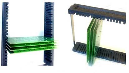
Assembled LED boards should not be stacked on top of each other and a correct
storage system should be used (Figure 7). To avoid the risk of damage to the
assembled LEDs, make sure that they are not exposed to compression forces of
any kind. Furthermore, the LED of the assemblies must also not be touched
directly.
Figure 7: Correct storage
2020-01-31 | Document No.: AN088 8/9www.osram-os.com
Don't forget: LED Light for you is your place to
be whenever you are looking for information or
worldwide partners for your LED Lighting
project.
www.ledlightforyou.com
ABOUT OSRAM OPTO SEMICONDUCTORS
OSRAM, Munich, Germany is one of the two leading light manufacturers in the world. Its subsidiary, OSRAM
Opto Semiconductors GmbH in Regensburg (Germany), offers its customers solutions based on semiconduc-
tor technology for lighting, sensor and visualization applications. Osram Opto Semiconductors has production
sites in Regensburg (Germany), Penang (Malaysia) and Wuxi (China). Its headquarters for North America is in
Sunnyvale (USA), and for Asia in Hong Kong. Osram Opto Semiconductors also has sales offices throughout
the world. For more information go to www.osram-os.com.
DISCLAIMER
PLEASE CAREFULLY READ THE BELOW TERMS AND CONDITIONS BEFORE USING THE INFORMA-
TION SHOWN HEREIN. IF YOU DO NOT AGREE WITH ANY OF THESE TERMS AND CONDITIONS, DO
NOT USE THE INFORMATION.
The information provided in this general information document was formulated using the utmost care; howe-
ver, it is provided by OSRAM Opto Semiconductors GmbH on an “as is” basis. Thus, OSRAM Opto Semicon-
ductors GmbH does not expressly or implicitly assume any warranty or liability whatsoever in relation to this
information, including – but not limited to – warranties for correctness, completeness, marketability, fitness
for any specific purpose, title, or non-infringement of rights. In no event shall OSRAM Opto Semiconductors
GmbH be liable – regardless of the legal theory – for any direct, indirect, special, incidental, exemplary, con-
sequential, or punitive damages arising from the use of this information. This limitation shall apply even if
OSRAM Opto Semiconductors GmbH has been advised of possible damages. As some jurisdictions do not
allow the exclusion of certain warranties or limitations of liabilities, the above limitations and exclusions might
not apply. In such cases, the liability of OSRAM Opto Semiconductors GmbH is limited to the greatest extent
permitted in law.
OSRAM Opto Semiconductors GmbH may change the provided information at any time without giving notice
to users and is not obliged to provide any maintenance or support related to the provided information. The
provided information is based on special conditions, which means that the possibility of changes cannot be
precluded.
Any rights not expressly granted herein are reserved. Other than the right to use the information provided in
this document, no other rights are granted nor shall any obligations requiring the granting of further rights be
inferred. Any and all rights and licenses regarding patents and patent applications are expressly excluded.
It is prohibited to reproduce, transfer, distribute, or store all or part of the content of this document in any form
without the prior written permission of OSRAM Opto Semiconductors GmbH unless required to do so in ac-
cordance with applicable law.
OSRAM Opto Semiconductors GmbH
Head office:
Leibnizstr. 4
93055 Regensburg
Germany
www.osram-os.com
2020-01-31 | Document No.: AN088 9/9You can also read