FPGA based modular control platform for switched mode power converters - Eindhoven University of Technology research ...
←
→
Page content transcription
If your browser does not render page correctly, please read the page content below
FPGA based modular control platform for switched mode
power converters
Citation for published version (APA):
Gerrits, T., & Eerd, van, M. J. M. (2010). FPGA based modular control platform for switched mode power
converters. In Proceedings of the IEEE Young Researchers Symposium, 29-30 march 2010, (pp. 1-6). Institute
of Electrical and Electronics Engineers.

Document status and date:
Published: 01/01/2010

Document Version:
Publisher’s PDF, also known as Version of Record (includes final page, issue and volume numbers)

Please check the document version of this publication:
• A submitted manuscript is the version of the article upon submission and before peer-review. There can be
important differences between the submitted version and the official published version of record. People
interested in the research are advised to contact the author for the final version of the publication, or visit the
DOI to the publisher's website.
• The final author version and the galley proof are versions of the publication after peer review.
• The final published version features the final layout of the paper including the volume, issue and page
numbers.
Link to publication

General rights
Copyright and moral rights for the publications made accessible in the public portal are retained by the authors and/or other copyright owners
and it is a condition of accessing publications that users recognise and abide by the legal requirements associated with these rights.

       • Users may download and print one copy of any publication from the public portal for the purpose of private study or research.
       • You may not further distribute the material or use it for any profit-making activity or commercial gain
       • You may freely distribute the URL identifying the publication in the public portal.

If the publication is distributed under the terms of Article 25fa of the Dutch Copyright Act, indicated by the “Taverne” license above, please
follow below link for the End User Agreement:
www.tue.nl/taverne

Take down policy
If you believe that this document breaches copyright please contact us at:
openaccess@tue.nl
providing details and we will investigate your claim.

Download date: 27. Feb. 2021
FPGA Based Modular Control Platform for
Switched Mode Power Converters
T. Gerrits Member, IEEE and M.J.M. van Eerd Member, IEEE
Electromechanics and Power Electronics Group
Eindhoven University of Technology, Netherlands
Email: t.gerrits@tue.nl, m.j.m.v.eerd@tue.nl
Abstract—In educational as well as research environments operating system drivers are available, and it is integrated
there is a demand for an easy way to prototype switching in the Matlab/Simulink software, which shortens development
converters. Several recurring standard tasks like pulse pattern time significantly. For basic PWM generation, the slave pro-
generation, driving controllable switches and analog to digital
conversion of physical quantities e.g. current, voltage and tem- cessor’s PWM module is sufficient. For more challenging
perature, need to be performed. Because these standard tasks modulation schemes, one will soon run into the limitations of
interfere with the research focus, a modular control platform for the standard dSpace system. A more advanced solution was
rapid prototyping is highly desirable. In this paper, a system is therefore chosen, namely the P25M DSP-FPGA board [2].
presented that provides an effective and flexible solution for these
requirements. In a typical application controling a SMPS, several recurring
subsystems can be identified. This property will be used to our
Index Terms—DSP, FPGA, Matlab, ARCP. advantage to create a library of configurable basic building
blocks that cut future development time. This enables the user
to focus on algorithm development instead of re-inventing the
I. I NTRODUCTION
wheel. Depending on the requirements, the user can fit the
I N order to operate a Switching Mode Power Supply
(SMPS) in its optimal operating point, closed loop control
is of vital importance. Dedicated Application Specific Inte-
required modules together to form a complete system that
will interface between the SMPS of interest, it’s physical
environment and Simulink.
grated Circuits (ASICs) are available for commonly used con-
To demonstrate the capabilities of the proposed system, an
figurations, such as buck or boost controllers (e.g. the LM3485
Auxiliary Resonant Commutated Pole (ARCP) Full Bridge
by National Semiconductor), but often a more advanced and
(FB) down converter with Synchronous Rectification (SR) has
flexible solution is required. Integrated environments capable
been designed. This specific SMPS has been chosen for its
of providing such a solution are for example dSpace [1], a
high efficiency when it is correctly controlled. That directly
Field Programmable Gate Array (FPGA), a Digital Signal
points out the disadvantage of the ARCP-SR-FB, as it requires
Processor (DSP), or a combination of DSP and FPGA [2].
ten active devices, which should each be controllable with an
Because Matlab/Simulink is the facto standard in R&D, it
approximated timing resolution of hundred nanoseconds. The
will be used as a development environment. To enable the
FB configuration utilized as a dc/dc down converter has been
user to implement new modules, the hardware architecture
presented in previous papers [5], [6].
should be as flexible as possible, and therefore the backbone
of the hardware will be an FPGA. Model Based Design is To ensure fast integration of the DSP-FPGA modular plat-
the Matlab/Simulink design flow, covering all necessary steps form in custom developed SMPSs, a set of switch driver boards
to convert a Golden Reference (GR, executable specification has been designed. With these boards, the most common
[3]) floating point model to fixed point bit and cycle true types of Active Semiconductor Devices (ASD) can be driven.
physical hardware. A test bench that was designed to check the Previous research on ASD gate driver circuits was presented
GR, can be used throughout the entire design flow to enable in [7], [8]. Data sheets and application notes on gate driver
continuous verification against the executable specification. ICs are also a good source of information, e.g. the IR2110
Xilinx integration with Maltab/Simulink: System Generator [9]. In this project, three types of gate driver circuits can be
(SG) further increases integration by enabling Hardware In identified, i.e. direct (low-side), high-side (together commonly
the Loop (HIL) testing. HIL enables the design running on known as half bridge configuration) and floating drivers.
physical hardware to be verified against the GR using the same The paper is organized as follows. An overview of the
test bench. Besides this, HIL goes even one step further; its implemented DSP-FPGA platform is given in Sec. II, and
possible to use additional hardware peripherals like ADCs, on details on the accompanying software modules are described
board RAM memory, MOSFET gate drivers etc., changing the in Sec. III. In Sec. IV the set of predesigned MOSFET drivers
test bench to the final in-circuit real-time application. is shown, required to drive the ARCP-SR-FB down converter
Various examples of system controllers based on the dSpace presented in Sec. V. Simulation and compilation results are
development platform have been presented [4]. The advantage verified in the experimental results Sec. VI, and conclusions
of e.g. a dSpace system is that it can be set up very fast, drawn from these results are stated in Sec. VII.Reference and display variables
II. H ARDWARE P LATFORM
Trouble free use of the platform can be achieved only if the
Non
requirements of the SMPS that needs to be controlled are met. isolated
PC interface card
Because these requirements are not known yet, the system has DSP FPGA ADC analog
been set up such that its overqualified for most SMPSs. The feedback
P25M board 4 signals
specifications set for this platform are listed in Tab. I.
32
The total hardware platform is divided into three parts,
namely the PC interface, the Isolation/Amplification, and the Differential signaling
input filter stage. An overview of the structure is depicted in
32 twisted pairs in SCSI cable
Fig. 1. Details on each of these modules are presented in Sec.
II-A, Sec. II-B, and Sec. II-C respectively.
Differential signaling
Table I
clk
S PECIFICATIONS H ARDWARE P LATFORM 23
Isolation board and input filter
4 4
Description Amplitude Max. Frequency Isolated
Digital Digital
Sigma delta
23 gate driver signals 0-18 V 40 MHz Isolator
modulator
Isolator
4 digital inputs 0-5 V 40 MHz
4 isolated analog inputs (14 bit) 0-5 V 78 kHz
4 non isolated analog inputs (16 bit) ±2 V 25 MHz 23
4 4
Third order
Input
Amplifiers low pass
regulator
filter
A. PC Interface Card
23
The PC interface card is designed to ensure high speed, 4 4
and error free communication from the P25M system to the To Analog Digital
MOSFET feedback feedback
outside world over a maximum distance of 5 meter, using drivers signals signals
a SCSI cable. This is achieved using three differential line
drivers (SN65LVDS389DBT) and one differential line receiver Figure 1. Schematic overview of hardware platform.
(SN65LVDS388ADBT, both [10]), each consisting of eight
channels. The LVDS drivers are powered by the PC’s common
power supply. The AD7401 is used in the 0-200 mV input voltage range,
and therefore ideally has a 14 bit resolution up to 78 kHz.
B. Isolation, Amplification and ADC board Whether this resolution is reached in practice depends on many
In order to supply the MOSFET driver boards in a safe way factors, e.g. adequate Printed Circuit Board (PCB) layout, and
and with adequate signaling, the isolation, amplification, and input filtering. The input voltage range is increased to 5 V by
Analog to Digital Converter (ADC) board (isolation board) means of a resistance divider network, the input impedance
was designed. It consists of a differential transceiver, an is increased by an operational amplifier (op amp) in voltage
isolation barrier, and an amplification stage. It is furthermore follower mode.
equipped with eight analog and four digital inputs, which are
designated as feedback signal from the SMPS to the P25M. C. Analog Input Signal Filter
The LVDS transceiver stage is complementary with the PC
interface card. As a result of the high ∂V
∂t present in SMPSs, and to avoid
The galvanic isolation in this system is required to en- aliasing, the analog signal which is fed back for control must
sure a high voltage dielectric isolation barrier between the be filtered before it is applied to the ADC. To retrieve the
PC and the SMPS, which is required for Safety Regulatory output voltage of the SMPS, a third order low pass filter with
Approvals (SRA) and reduction of Electro Magnetic Compat- a cut-off frequency of 7 kHz is designed. This filter is added
ibility (EMC) issues. The SRA is a guideline to guarantee to the system as a separate board because the analog filter
safe design of equipment that is directly connected to 230 requirements are different for each application.
Vac or industrial power systems, which is the case here.
Regarding EMC, the galvanic isolation reduces common mode
III. FPGA S OFTWARE M ODULES
and ground loop problems. The isolation is accomplished for
digital signals by using the Si8460 devices [11], and for the In the scope of the modular platform, the minimal set of
ADCs using the Isolated Sigma Delta Modulators (ISDM) modules consists of analog inputs, control and pulse pattern
AD7401 [12]. On the digital side of the ADC a clock pulse generation. Initially FPGA development has been our focus.
of 20 MHz is applied, and a 1 bit data stream with an For future advanced control algorithms the floating point DSP
average proportional to the analog input voltage is retrieved. will need to be used, [13].A. ADC several MOSFET driver boards were designed to drive gates
For selecting suitable ADCs, several aspects are considered directly, i.e. in half bridge configuration (low side & high
like sample rate, resolution and analog to digital side isolation. side), and galvanically isolated. All gate drivers are built to
For each selected ADC a dedicated FPGA module will be support dynamic driving i.e. switched on and off at the typical
written. The AD7401A was selected because of it’s internal switching frequency without the need for 50 % duty cycle (D).
galvanic isolation barrier. The interface from the FPGA to the In the galvanically isolated drivers, this is achieved by the dc
ADC is pretty straightforward. A Clock signal (up to 20 Mhz) decoupling capacitor in series with the transformer (Fig. 2).
is generated on the FPGA and per clock cycle, one bit of data A restriction on D, 0.1 ≤ D ≤ 0.9 is a result of this method.
is captured. In order to use this signal, decimation is usually The output voltage (Vout ) will otherwise exceed the typically
required. Because every application has it’s own requirements allowed gate source voltage of the power MOSFET. The direct
of resolution and/or sample rate, the decimator is configurable. drives are furthermore able to drive in static mode (on or off
for sustained periods of time). As needs appear, more driver
B. Pulse pattern generation boards will be designed to perform required tasks.
By studying the topology of the converter, all required
V+
sequences to control switches can be determined. Some events
will require a highly accurate adjustable timing reference.
Because of the discrete nature of FPGA technology, the gate1
dithering technique presented in [14] could be implemented to
Vout
increase resolution. Ordinary counters are the preferred way to
implement less critical fixed delays such as dead-time insertion gate2
for safe operation of a half bridge. Switching frequencies are V-
typically in the kHz to several MHz range.
1) Development flow: In order to compensate for differ- Figure 2. Half bridge floating gate driver circuit.
ences in driver delays, the delay from FPGA output to the
actual MOSFET switching moment has to be measured. Both
The functionality of the ARCP and SR MOSFET drivers is
rising and falling edges (turn on and turn off) should be
identical (Fig. 2), their designs however differ slightly due
measured as they are different as depicted in Fig. 7. Also high
to different requirements. The MOSFETs that need to be
and low side half bridge drivers can use nonidentical circuitry
driven by the SR driver have a much higher input capacitance,
and therefore will have different timing properties.
resulting in higher transformer currents. A transformer with a
By means of an initialization script the measurement values
lower Equivalent Series Resistance (ESR) is therefore chosen.
are rounded to integer numbers of clock cycles, in fact
The driver consists of an level shifter and a half bridge stage.
constants that allow efficient hard coding on the FPGA.
Because the output signals of the isolation stage are 0-10
In the used power converter, every controlled timing event
V, the NMOS cannot be driven directly, the level shifter is
is referenced to a master clock. The demo power converter
included for that. The series resistor on the secondary side of
roughly features two groups of timing events related to each
the transformer reduces current peaks during transitions, the
other by means of the phase shift between the full bridge legs.
parallel resistor is for pull down and the zener diodes protect
Within each group all events can be referenced to each leg’s
the gate of the power MOSFET against over voltage.
50% duty cycle. For efficient implementation on the FPGA,
all timing events within a group are referenced to the first
V. ARCP-FB-SR DOWN CONVERTER
event occurring in the group. The succeeding events will then
accordingly be just simple integer numbers of clock events Fig. 3 shows the proposed converter topology, and Tab. II
delay. shows the specifications set for this demo converter. The basic
The actual group-timing that is generated on the FPGA is principle of the FB dc/dc converter is that an AC voltage is
the desired timing plus the driver delay compensation. created across the primary of a transformer, and this voltage is
2) Forbidden state prevention: When controlling a half rectified on the secondary side (PMC [15]). The input voltage
bridge, care must be taken that the both switches on state (Vin ) and winding ratio (k) of the transformer determine the
never occurs. When the FPGA is being programmed through maximum value of the Vout . Each of the switches is turned on
JTAG, or reset and loading from the configuration PROM, for half the cycle time, minus a small period of dead time in
the FPGAs I/O Pins are put in a tri-state condition. Because between. Switches S1 and S4 are simultaneously on, just like
the used LVDS buffers don’t support tri-state signalling, S2 and S3 , By varying the phase angle between S1,4 and S2,3 ,
programmable pull up/down or jumpers are used to define the effective voltage across the transformer can be adapted,
default/unharmful/safe signal states. In this manner the FPGA and with it the output voltage. The ARCP and SR circuits are
can be reprogrammed without problems, while being perma- added to the FB converter to increase its efficiency over the
nently connected to a fully powered SMPS. full output power range.
The ARCP [16] circuit is used to minimize the switching
IV. MOSFET D RIVERS losses by ensuring Zero Voltage Switching (ZVS). When
The proposed FPGA platform, allows drivers up to 40MHz switching the points A and B alternating between 0 and Vin ,
to be driven directly. In order to operate the power converter, the voltage difference is Vin /2 with middle point M, whichS1 S3 Ss1
LO conduction losses.
Vin M
LA + Vout When taking all dead times (FB Dt, ARCP Dt, and Syn-
VSR snub2
snub1
Sa1 Sa2 A +
VAB - Rec Dt) into account the actual implementation sequence
Sa3 Sa4 B - shows the complexity of the 16 gate drive signals (Fig. 4).
LB In each family of colored, numbered dots, all four timing se-
S2 S4 Ss2 quences have been identified. By regarding the order of events,
one can clearly see that an asymmetry is present between the
Figure 3. The proposed ARCP-FB-SR down converter. sequences referenced to the right and left leg. Because the first
event that occurs is switching off the synchronous rectifier in
the right leg, this is the event to which all others in this family
is constant at Vin /2. If for example the voltage at point A are referenced to. In order to prevent a phase shift, the timing
must be transitioned from 0 towards Vin after S2 has opened of the left leg has to be compensated for it by adding an extra
and before S1 has closed, i.e. during the dead time (td ), Sa2 delay (and virtual event) to which al timing in the right leg
must be on. Due to the voltage across the inductor La being families is referenced to.
Vin /2, the resonant commutation phase between La and the
drain source capacitance (Cds ) of S1 and S2 is initiated. The Idealized timing from topology study
V_bus FB_LL
snubber circuit snub1 is included to reduce the voltage peaks 0 FB_RL
across the ARCP switches which are a result of resonance Phi
caused by La,b together with the Cds of Sa1−4 . V_bus
The principle of SR aims at reducing the secondary rectifier
0 V_AB
-V_bus
losses by turning the MOSFET on during conduction of its Switching Period
anti-parallel diode [15]. The typical forward voltage drop is Active ARCP_LL_Ri
0.7 V for a small signal diode, and around 1.5 V for a high Not Active ARCP_LL_Fa
ARCP On Time
power device when the nominal output load (Rload ) of 2.3 Ω Active ARCP_RL_Ri
is considered. This would result in a conduction loss of 16 Not Active ARCP_RL_Fa
W per device. If during conduction of the diode the devices ARCP On Time
Ss1,2 are turned on, the conduction losses can be reduced. Active
Not Active
SynRec_Pos
SynRec_Neg
The on resistance (Rds(on) ) of the devices should therefore be Actual implementation with dead times
lower than 70 mΩ. The device chosen (Tab. II) has an typical Active
2 5 2 5
FB_LL_Hi
Rds(on) of 5 mΩ reducing the conduction losses to 1.1 W Not Active FB_LL_Lo
per device. The snubber circuit snub2 is included to reduce
FB_Dt
Active FB_RL_Hi
the voltage peak across the SR switches which are a result of Not Active
4 6 4 6
FB_RL_Lo
resonance caused by the secondary leakage inductance of the FB_Dt
0 2 Left Leg Timing
transformer together with the Cds of Ss1,2 . V_bus
0 V_AB
-V_bus
3 6 Right Leg Timing
Table II
S PECIFICATIONS ARCP-FB-SR DOWN CONVERTER I_ARCP_LL_Ri
0
I_ARCP_LL_Fa
Parameter Nominal value Parameter Value/device 0
I_ARCP_RL_Ri
I_ARCP_RL_Fa
Vin 400 V k 7:1:1
Vout 48 V LA,B 8 µH
fsw 100 kHz S1−4 STW45NM60 Active
0 1 3 7 8
ARCP_LL_Ri_Hi
Pout 1 kW Sa1−4 STP10NK60 Not Active ARCP_LL_Ri_Lo
Rload 2.3 Ω Ss1,2 IRFP4568PbF Active
0 1 3 7 8
ARCP_LL_Fa_Hi
Not Active ARCP_LL_Fa_Lo
ARCP_Dt
Active ARCP_RL_Ri_Hi
2 5 7 88
Not Active ARCP_RL_Ri_Lo
From the topology it is clear that the controlling degree of Active ARCP_RL_Fa_Hi
2 5 7 8
freedom is the phase shift (Phi) between the left and right Not Active ARCP_RL_Fa_Lo
leg of the full bridge. In each leg, during the dead-time of
Active SynRec_Pos_Hi
the corresponding FB leg, the ARCP circuit is activated to Not Active
4 6 1 3
SynRec_Pos_Lo
make sure that before the dead time has ended, the voltage Active SynRec_Neg_Hi
4 6 1 3
of the MOSFETs has been adjusted in such a way that ZVS Not Active SynRec_Neg_Lo
at turn on is achieved. The turn off of the ARCP circuit is SynRec_Dt
less critical but should occur between the leg enters the next Figure 4. Gate timing for the ARCP-FB-SR down converter.
dead time interval. When the voltage across the terminals of
the transformer (VAB ) is positive, the MOSFET, of which
the internal anti-parallel diode as result of the applied voltage Efficiency simulations on the proposed circuit were per-
should conduct (Ss1 ), is switched on to reduce semiconductor formed in the configurations FB only (FB), FB with ARCP(FB-ARCP), FB with SR (FB-SR), and with the total circuit
(ARCP-FB-SR), with an constant Rload and for the indicated
values of Vout (Tab. III). For both the simulated and measured C C B
efficiency, the topology efficiency is considered, excluding A
power consumption by control and driver circuits. From the re-
sults shown in this table it can be concluded that for maximum
efficiency, the ARCP-FB-SR is the optimal configuration.
What can also be recognized is that the same efficiency is In
simulated for high output power in the FB-SR and ARCP-FB-
SR configuration. This is the result of the high transformer
current that ensures ZVS in the FB-SR configuration, the
ARCP can therefore be turned off at nominal output power.
Table III
Out
S IMULATED EFFICIENCY OF GIVEN CONFIGURATIONS FOR VARIOUS Vout
1 A
B
Efficiency [%]
Vout FB FB-ARCP FB-SR ARCP-FB-SR
6V 34 79 33 85
12 V 40 82 65 95
24 V 58 89 82 97
48 V 81 94 97 97
VI. E XPERIMENTAL R ESULTS 2
A
In order to demonstrate the potential of the system, all
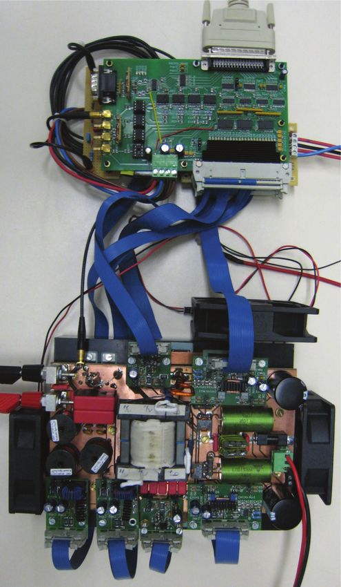
described system parts were assembled in a prototype. A
picture with all the indicated parts is shown in Fig. 5. The
sizes of the isolation board and ARCP-FB-SR down converter C
are 100 x 160 mm, and 160 x 200 mm respectively. B
To verify whether the implemented PC interface and isola-
tion board meet the high frequency requirements set in Tab. From PC
I, measurements were carried out. A block shaped wave was interface
applied to an input of the PC interface, and on the isolation
board the corresponding output signal (Vgate ) was fed back as Figure 5. The build ARCP-FB-SR (1), and isolation board (2). The shaded
digital input. The resulting signals measured at the output of areas indicate for 1: MOSFET drivers of ARCP (A), FB (B), and SR (C), and
for 2: amplification (A), isolation (B), and ADCs (C).
the PC interface (Vinter ) are depicted in Fig. 6 for the specified
frequencies. Typical rise and fall times of Vinter are around 2
ns, variation of the duty cycle is caused by the inaccuracies
in the input signal. 4
Amplitude [V]
Timing delays as described in Sec. III-B1 were measured,
2
0
Fig. 7 shows an example of the difference in rise and fall times
of the SR MOSFET gate voltage. Timing compensations was
4
added in the FPGA to ensure correct operation of the SMPS.
Amplitude [V]
2
The total system efficiency was measured for the configura- 0
tions FB, and FB-ARCP only, the timing of the SR driver was 0 20 40 60 80 100 120 140 160 180 200
Time [ns]
not correctly programmed and the component was excluded 4
Amplitude [V]
therefore. The gate and source of the SR drivers were short 2
circuited, and their diodes were used for rectification. Tab. 0
IV shows the results of the measurements. From these results
it can be concluded that for high output powers, the ARCP 4
Amplitude [V]
circuit already increases efficiency. Although, the programmed 2
ARCP timing is not yet optimal, efficiency at lower power 0
levels is expected to increase after timing improvement. 0 10 20 30 40 50
Time [ns]
60 70 80 90 100
The thermal stability of the SMPS was also measured,
the temperature of the transformer depicted in Tab. IV was Figure 6. Vinter for approximately 5, 20, 30, and 40 MHz.
measured after 30 minutes of operation, and was stable.20
SynRec_Lo
SynRec_Hi R EFERENCES
SynRec MOSFET gate
15
[1] “http://www.dspaceinc.com,” Internet, dSpace Inc.
[2] “http://www.innovative-dsp.com,” Internet, Innovative Integration Inc.
10
[3] “http://www.mathworks.com/,” Internet, The MathWorks Inc.
Voltage [V]
[4] G. Cao, L. Lin, H. Qiu, and J. Pan, “Design and analysis of a dSPACE-
5
based position control system for a linear switched reluctance motor,”
in Power Electronics Systems and Applications, 2009. PESA 2009. 3rd
0
International Conference on, 2009, pp. 1–4.
[5] O. Patterson and D. Divan, “Pseudo-resonant full bridge dc/dc con-
−5
−1 −0.5 0 0.5 1 1.5 2 2.5 3 3.5 4 verter,” IEEE Transactions on Power Electronics, vol. 6, no. 4, pp. 671–
Time [s] −6
x 10 678, 1991.
[6] R. Redl, N. Sokal, L. Balogh, and S. Elfi, “A novel soft-switching full-
Figure 7. SR MOSFET driver and gate signals. bridge dc/dc converter: analysis, design considerations, and experimental
results at 1.5 kW, 100 kHz,” in Power Electronics Specialists Conference,
1990. PESC’90 Record., 21st Annual IEEE, 1990, pp. 162–172.
Table IV [7] J. Strydom, M. de Rooij, and J. van Wyk, “A comparison of fundamental
M EASURED EFFICIENCY OF GIVEN CONFIGURATIONS FOR VARIOUS Vout gate-driver topologies for high frequency applications,” in Applied Power
Electronics Conference and Exposition, 2004. APEC’04. Nineteenth
Efficiency [%] Temperature Transformer [◦ C] Annual IEEE, vol. 2, 2004.
Vout FB FB-ARCP FB FB-ARCP [8] T. Lopez, G. Sauerlaender, T. Duerbaum, and T. Tolle, “A detailed
analysis of a resonant gate driver for PWM applications,” in Applied
6V 38 37 102 97 Power Electronics Conference and Exposition, 2003. APEC’03. Eigh-
12 V 62 61 72 69 teenth Annual IEEE, vol. 2, 2003.
24 V 86 89 50 56 [9] “IR2110, HIGH AND LOW SIDE DRIVER,” International Rectifier,
48 V 92 94 40 36 pp. 1–18, 2005.
[10] “http://www.ti.com,” Internet, Texas Instruments Inc.
[11] “http://www.siliconlabs.com,” Internet, Silicon Laboratories Inc.
[12] “http://www.analog.com,” Internet, Analog Devices Inc.
[13] F. Rodriguez, S. Cobreces, E. Bueno, Á. Hernández, R. Mateos, and
F. Espinosa, “Control electronic platform based on floating-point DSP
VII. C ONCLUSION and FPGA for a NPC multilevel back-to-back converter,” Electric Power
Systems Research, 2008.
By utilization of this modular platform, SMPS projects can [14] M. Zamora and M. Henry, “Fpga implementation of frequency output
be prototyped faster in the future. and input using handel-c,” Industrial Electronics, ISIE 2007. IEEE
International Symposium on, pp. 2313–2318, 2007.
The first software modules implemented show that fast [15] D. Jain, P. Jain, and H. Zhang, “Analysis and design of an auxiliary
integration with a SMPS is possible, the library of modules can commutated full bridge DC/DC converter topology including the effect
be extended to support specific needs. Additional effort must of leakage inductance,” in INTELEC. IEEE; 1998, 2002, pp. 15–15.
[16] R. De Doncker and J. Lyons, “The auxiliary resonant commutated
be put in FPGA programming to remove timing problems, and pole converter,” in Industry Applications Society Annual Meeting, 1990.,
finalize full circuit measurements. Conference Record of the 1990 IEEE, 1990, pp. 1228–1235.
The designed MOSFET drivers work as intended and they
can be used in future projects. Verification on ZVS and
correct SR operation as well as efficiency measurements for
all configurations should be added to the results.
In order to completely use the P25M board’s potential,
the correct combination of software package versions of six
different vendors has to be installed.
Although our suggested isolated delta sigma ADC has
several advantages, it also features impairable down sides.
In order to obtain sufficient resolution, the bitstream has to
be decimated. This means that during the interval needed
to obtain the required resolution, switching events in the
power converter can occur. Without taking measures, this
will result in excessive amounts of unwanted switching noise.
By utilizing the positional degree of freedom of the ADC’s
sampling moment, switching noise can be minimized.
ACKNOWLEDGMENT
The authors would like to thank dr. D. V. Malyna, dr. J.L.
Duarte, and ir. M.A.M. Hendrix for their helpful suggestions
and fruitful discussions. Also many thanks go out to ir. M. G.
L. Roes and R. J. W. de Groot for their assistance during the
measurements of the system.You can also read