Design of bang-bang controlled dc-dc buck converter integrated with LDO
←
→
Page content transcription
If your browser does not render page correctly, please read the page content below
Design of bang-bang controlled dc-dc buck
           converter integrated with LDO

Thesis submitted according to the partial requirements for the
                         degree of

         Bachelor of Technology (HONS)
                             In
               Electrical Engineering

                             By
               Rajeev Kumar Dokania
                  Roll No-9918114
                   Under The Guidance of
                Prof. Shri Amit Patra

          Department of Electrical
                 Engineering
  Indian Institute of Technology Kharagpur
         Kharagpur –721302, INDIA
                  May, 2003

                              1
Department of Electrical Engineering
               Indian Institute of Technology Kharagpur
                      Kharagpur-721302, INDIA
                               May, 2003

                                  CERTIFICATE

This is to certify that the thesis entitled “Design of bang-bang controlled dc-dc buck
converter integrated with LDO.” is submitted in partial fulfillment of the requirements
for the award of the degree of Bachelor of Technology (Hons.) in Electrical Engineering
at the Indian Institute of Technology, Kharagpur.
     It is a faithful record of bonafide research work carried by Mr. Rajeev Kumar
Dokania (Roll No. 9918114) under our supervision and guidance. It is further certified
that no part of thesis has been submitted to any other University or Institute for the award
of any other Degree or Diploma.

Prof. Amit Patra
Associate Professor
Department of Electrical Engineering
Indian Institute of Technology Kharagpur
Kharagpur – 721302, India

                                             2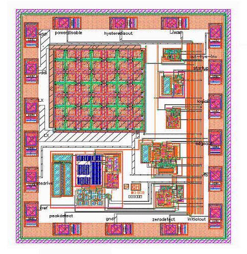
Acknowledgement

       I thank Prof Shri Amit Patra for providing me with this wonderful opportunity. I

am delighted that he not only offered to be my final year project guide, but also let me

work on things, I was very keen on working. He has been very patient with me and was

ever ready to listen to me. I used to go to his room whenever I was finding him there.

Even after being so busy he was always there to listen to me, to encourage me, and being

more and more demanding. He has helped me learn a lot. Under his guidance I have

learnt things; I wouldn’t have ever imagined I would be doing once. Sincerely thank you

sir, thank you very much.

       Special thanks go to Mr. Shailendra Kumar Baranwal, for helping me

understand things properly. He made me realize what all are the things one should take

care of while designing a circuit, a knowledge that has been very valuable for me,

furthermore he has been very helpful to me while doing the layouts

       I must thank Mr. Ravinder Pal Singh, for giving fundaes about the layouts, and

helping me out whenever I was in a need for help. He has helped me out while doing the

design submission, debugging those 10,147 drc errors. Thanks once again. Special thanks

to Mr. Syed Asif Eqbal and Mr. Ershad Ahmed for I have used their layout for the

PMOS switch and the hysteresis comparator.

       Lastly I would like to thank my friend Mr. Padmanava Sen and Mr. Vipul Garg

for giving me important tips on layout design. I must thank all of my friends, for very

patiently sharing with me my excitement, whenever I realized a circuit successfully.

                                            3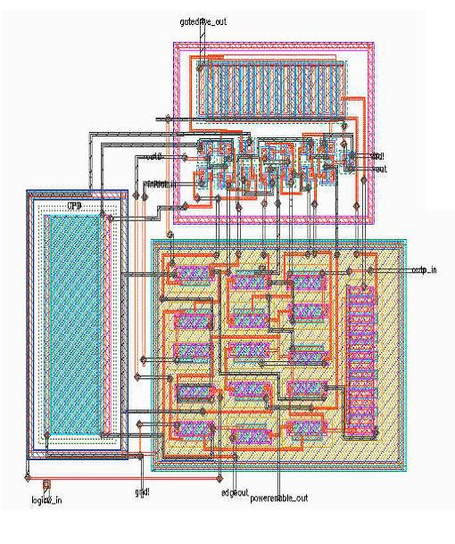
Synopsis
Title               Design of bang-bang controlled dc-dc buck converter
                     integrated with LDO.
Candidate            Rajeev Kumar Dokania
Roll Number          9918114
Degree               B.Tech. (Hons) in Electrical Engineering
Project Guide        Prof. Amit Patra
Institution          Indian Institute of Technology Kharagpur
                     Kharagpur – 721302, India

Signature of the Guide                              Signature of the Candidate

Prof. Amit Patra                                  Rajeev Kumar Dokania
Date:                                             Date:

                                        4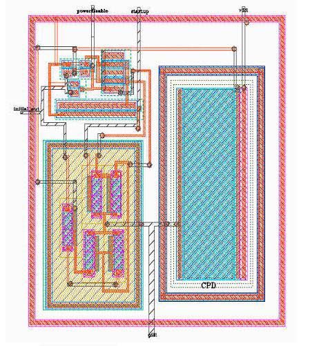
Table of contents

1. Introduction………………………………….................06
2. Design of DC-DC converter Blocks……………………16
3. DC-Dc Buck converter, the final circuit………………38

4. LDO topology and DC-DC integrated with LDO……...43

5. Conclusion……………………………………………....49
6. Appendix…………… …………………………………..53
References………………………………………………....62

                          5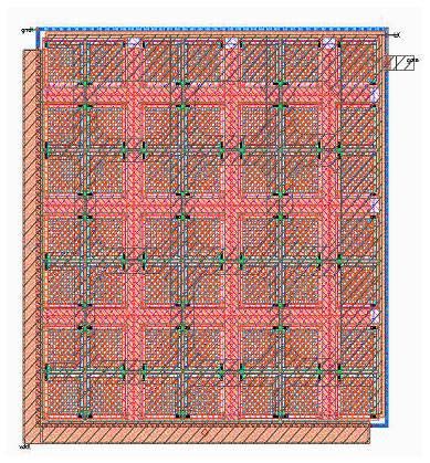
1. Introduction:

Power supplies are the most important and fundamental aspect of an electrical system.
For most of the integrated circuits (ICs), the input supplies are derived from already
available dc supplies like batteries, but these supplies are generally noisy and are not
stable, worst they show large variations with the load. Modern state-of-the-art
technologies put stringent requirements on the power supplies, and regulators are
designed to meet these objectivities. A good power supply is expected to have these
characteristics.
    •   should be ripple free
    •   should be able to give regulated voltage supply at high load
    •   should be very efficient
    •   The transient response i.e. change of voltage with the sudden change of load
        should not be much.
    •   Should work with large input voltage variations, as most of the time the ICs work
        on lithium batteries, the range of voltages for which is very high. So its highly
        desirable that we extract most out of the battery.
    •   The line regulation and the PSRR performances should be good
    •   The no load power consumption should be practically zero.

So as we go for designing a regulator module these 7 make up the performance
parameters that need to be taken care of…
In battery operated system we can think of two kinds of regulator modules.
    1.) linear Regulators (LDO)
    2.) switching type(SMPS)

                                              6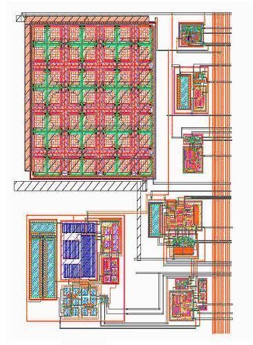
1.1) LDO regulator
Linear regulators or series regulators, use a pass switch between input and output, an
error amplifier and a reference voltage. The blocks are so connected such that the
conductance of the pass device can be modulated to maintain nearly constant output
voltage regardless of supply voltage and load current variations.

                                1.2) Switching regulator
Switching type regulators are the mixed mode circuits, where the feedback loop employs
mixed signal i.e. both analog and digital. In case of ICs mostly dc-dc converters are used
and typically the dc-dc converters are comprised of a PWM controller, switches,
capacitors, diodes and inductors. The switching type regulators can be used even without
the inductances (e.g. employing the charge pump circuits), but they normally can’t be
operated for large currents.

                          1.3) Which one is better? : Tradeoffs
In switching type regulators the output is not ripple free. They induce substantial noise on
the output voltage and generally don’t have a good load dump characteristics. The output
voltage will be having ripples. And as we go for decreasing that ripple the switching
frequency requirement will go up so will the switching losses and also the substrate
noises. Thus once forced for ripple free performance the switching type regulators fail to
deliver. The linear regulators respond faster to the load dumps, are less noise sensitive
and give a ripple free performance. The LDO regulator has a good ripple free
performance a good PSRR and a good line regulation thus ripple performance wise the
linear regulators are better.
      In terms of power efficiency, Switching regulators are very power efficient with the
efficiency in the range of 80 to 95%, but for the linear regulators the maximum power
efficiency that a 3V linear regulator can achieve with a 6V power supply is just 50%.
Thus that means that linear regulators are the worst when the efficiency is considered.
But that is not actually the case the efficiency of the linear regulators improves
significantly as the difference between the output and the input voltages goes down, but

                                             7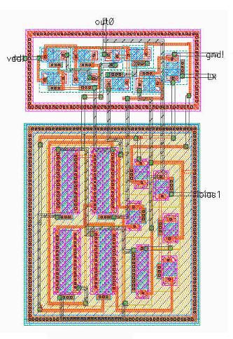
this minimum difference is again limited by what is called the dropout voltage of the
linear regulator. And hence a low drop-out regulator is desired.

                                       1.4) Demand
Both the types of regulators have certain advantages over others and depending upon the
requirements one is preferred over other, while sometime both are cascaded to give the
best of both the world.

                          Fig1.4.1 the performance-preference chart

Thus as is evident from the chart above whenever efficiency is the main constraint the
SMPS is the obvious choice, e.g. the desktop microprocessors benefits from the large
efficiency of the SMPS, while drawing large current at high input–output voltage
differences. Whereas high performance analog circuit blocks prefer low noise and cost-
effective linear regulators, but with the advent of portable equipments like cellular
phones, pagers, laptops, the requirement and coexistence of both the regulator is
necessary. In these applications, the power management IC drives noise sensitive circuits
from relatively high input supply voltages. The switching type regulator regulates this
voltage down to a value near about the output voltage…and thereafter the linear regulator
block regulates it to the low noise output voltage. This way the topology benefits from

                                             8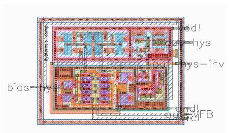
both, the high efficiency of the switching type regulator and the good noise performance
of the linear regulators….

                             Fig1.4.2 the SMPS and LDO cascaded
Thus we find that as we place more and more stringent requirements on the regulator
modules. We need to go for a realization where the switching type regulators and the
linear ones both need to play their part. In next chapters the design of both the Switching
type regulator and the LDO will be taken care of.

                1.5.) Design of Switching type regulators.
The design and control of a DC-DC Buck Converter is an active research area both in
automatic control theory and power electronics. The idea behind the design is to get a
complete on chip DC-DC Buck converter (excluding the inductor, output capacitor and
the diode). Most of the commercially available DC-DC Buck converter chips are based
on the PWM (pulse width modulated) control technique and suffer from the high value of
the no load current. The present design is an attempt to improve the converter’s no-load
current requirement using Constant Volt-Secs Bang-Bang control scheme. This scheme

                                            9
has the unique future of high efficiency during moderate loads as well as a very low value
of current consumed by the chip during the no-load condition. The present target of the
design is to reduce the no-load current down to 8µA. This type of converter is of great
importance in the mobile devices where the complete circuit is in the active mode for
very small durations and hence the converter works under almost no load condition for
most of the time. So any little saving in power will enable us to use the same battery for
longer durations without recharging. Furthermore the design works on the logic
determined by the peak current detector and the zero-crossing detectors .thus there is no
need for any oscillator here. The oscillator usually is the most power consuming in no lad
condition and hence by avoiding it we will be economizing on power, further the
substrate noises in this case will be lesser. This kind of scheme is better than most
common PWM based drive. The efficiency of the regulator overall is very high, more so
during no load condition and hence finds its applications in mobile industry where the
cell operated mostly in no load condition, further the lithium battery used there is very
costly and hence a power efficient regulator is desired. From this point of view the
scheme just proposed is better.
1.6) BASIC
Fig1.6.3 The topology of the Buck converter
10Consider the circuit shown in Fig-1.6.3. It shows the common buck converter topology
along with a block level representation of the control circuit. The converter has got two
state variables, viz.: the inductor current and the capacitor voltage. The objectivity of the
control circuit is to help achieve these state variables those values that are desired from
user point of view. Here for example, the output voltage i.e. the capacitor voltage is the
desired quantity and it should maintain a fairly constant value irrespective of the load or
supply variations. The control circuit achieves this by changing the state of the MOSFET
switch which in turn changes the structure of the system. When the switch is ON, E is
connected to inductor and diode is OFF. On the other hand, when the switch is OFF, E is
not connected to any other part, but the state of diode will depend on whether the
inductor current is continuous or not. If the inductor current is continuous, diode is ON,
otherwise it is OFF. So we see that there are three different possible configurations and
the corresponding system equations are as follows:
• Configuration I: PMOS ON, DIODE OFF
In this configuration the current across the inductor ramps up with a slope of (E-Vout)/L,
while the voltage across the capacitor also increases as the charging current flows across
it, though the voltage discharge operation is also there due to the load connected across
the capacitor.
• Configuration II: : PMOS OFF, DIODE ON
In this configuration the current across the inductor ramps down with a slope of (–
Vout)/L, while the voltage across the capacitor still builds up as the average current
across the capacitor is still positive, though here again due to load connected across the
capacitor the discharging will be there, but if the load current is less than Ip/2 (as is the
case in my scheme), then in this configuration also the voltage will build up.
• Configuration III: PMOS OFF, DIODE OFF
In this configuration both the PMOS and the Diode is off , and hence the inductor current
is zero, so no charging current will be there across the capacitor and hence the capacitor
voltage will decay depending upon the load current.
11Here while configuration I & II occur when the circuit is acting in mode 1, the
configuration III occurs while the circuit is acting in mode 2.
1.7) Scheme
We see that if switch goes through a whole cycle of Ton and TOff then inductor current
changes from I1 to I2 and comes back to I3. I3 and I1 need not be always same, but can
be made so. In fact, during the steady state operation of the converter, I3 should come
down to I1. The control circuit that is shown in Fig-1.6.3, precisely does this and not only
this, it also keeps value of I1 (=I3) and I2 fixed. The waveform of inductor current is
shown in Fig-1.7.1. It is a triangular waveform with base at zero and vertex at Ip. So we
find that I1 is kept at zero and I2 at Ip (peak value of the triangular current waveform). It
should be noted that for this type of control of inductor current, there is no state of
Config-3. This type of current conduction is called just discontinuous conduction.
To achieve it, we use a peak-current detector and a zero-crossing detector,
with these two as input, the control logic gives the appropriate gate pulses so that at no
time the transistor current exceeds its rated value (Ip). Now let’s come to the output
voltage Vout. Suppose at some instance of time when the circuit is operating in MODE-I,
with each of the triangular pulse of current in the inductor, capacitor will get charged
with that much amount of electric charge in each of those pulses. The rate of rise of
capacitor voltage will be proportional to the difference between this charging rate and the
discharging rate due to the load connected to C. As inductor current always oscillates
between zero and Ip, its average value is Ip/2. By design, this value is kept more than the
full load requirement. So there exist a positive difference between rate of charging and
rate of discharging and this difference increases as the load is reduced. This difference
will led to a gradual increase in the capacitor voltage.
Now consider the situation when instead of a fixed value of Vout, we allow a
band of ±∆V about Vout. So to control the output voltage within this band, the output
voltage is fed back to a Hysteresis Comparator (Also know as Schmitt Trigger) as shown
in fig-1.6.3. A Hysteresis comparator has got two different trip points for rising input
voltage (here our input is our Vout) and falling input voltage. As Vout rises due to the
difference in the charging and discharging rates of the capacitor, at the upper trip point of
12Vout + ∆V, Hysteresis comparator disables the gate-drive signal and the circuit operates
in MODE-II. While in MODE-I, the drive is determined from the peak-detector’s and the
zero-crossing detector’s output, The two modes differs in that the pass device is
continuously switched ON and OFF with Ton and Toff periods in MODE-I, it is
completely switched OFF in MODE-II. So MODE-I comes with a burst of pulses
whereas MODE-II doesn’t have any and the switch is always OFF. The circuit remains in
Config-3 as long as it is in MODE-II. In MODE-II, as there is no charging of the
capacitor, its voltage falls down as the load is always there. As soon as it crosses the
lower trip point (Vout – ∆V) of the Hysteresis comparator, the peak-current detector and
the zero-crossing detector as well as the previous state of the latch that is there in the
control circuit determines the gate drive signal and the converter again enters MODE-I.
This cycle of MODE-I and MODE-II goes on and we get the output voltage within our
range of V ±∆V.
Fig1.7.1 the typical performance characteristics
131.8) Advantages of Constant Volt-Secs Bang-Bang Control (without
oscillator) scheme:
• No reverse recovery losses( ZERO current switching)
At the end of each cycle, the inductor current always comes to zero level. So even if
the whole of E is applied at the beginning of Ton, there will not be any reverse
recovery losses in the diode. So reduction in losses gives a high efficiency during
loaded conditions.
• Zero losses at low load condition
We have seen that there are two modes of the converter. Only MODE-I requires
pulses from the oscillator. So even if oscillator is switched OFF during MODE-II,
there in no harm in it. In the entire control circuitry, oscillator consumes maximum
current, and a sleeping oscillator means a lot of power saving. The saving is not much
when the load is at its highest, but as the load too goes to the sleep mode, the
converter remains mostly in MODE-II and then saving will be quite substantial.
Therefore this saving may actually surpass even the first one.
• Low substrate noise
As we are not using any oscillator here, it adds to our advantage as when in mode2,
there isn’t any switching and hence no substrate noise will be there. But had the
oscillator been there would have been considerable substrate noise.
• Power saving due to no oscillator
As the switching decisions are taken based on just the peak-detector and the zero-
crossing detector, thereby obviating the need for oscillator. The topology is very efficient
during low load conditions as mostly oscillator is the main lossy element at no load
condition.
• Suppression of load or supply line effects
Due to the use of the Hysteresis comparator and an independent Voltage Reference,
the output voltage is free of any load or supply line effect.
141.9) Specification for the converter design
• can support a load current of up to 220mA
• Supply voltage variation between 4.5 to 9V
• Output voltage- user defined, between 1.3V to input voltage
• Quiescent current 8uA
• 18 pin- DIP package
• Estimated 1.5mm*2mm chip area
1.10) Different blocks used
• Band-gap reference
• Current source and sinks
• Peak current detector
• Zero crossing detector
• Hysteresis comparator
• Pmos switch
• Startup circuit
• Control block
• Gate-drive circuit
152.) Design of Dc-Dc converter Blocks
2.1Band-gap reference
Fig2.1.1 the basic architecture
The Guiding equations:
I*R=Vt * ln(n)…………………….(2.1)
Vbe+k*m*R*I=Vref……………….(2.2)
Fig2.1.2 Vbe and Vt variation with temperature
Thus if, m1+ s*m2=0;
We have k*m*ln(n)= s; for design to be temperature insensitive.
16Startup-why?
¾ I=0, is also a stable operating point.
Explanations:
The purpose of the voltage reference is to provide a constant reference voltage
independent of temperature or the supply voltage and also the process. The principle of
the band-gap voltage reference is to balance the negative temperature coefficient of a PN
junction with the positive temperature coefficient of the thermal voltage Vt = kT/q. The
Vbe shows a drop of 2mv/degree Celsius while the thermal voltage increases at a rate of
0.085mv/degree Celsius. This fact is utilized while designing the band-gap reference
circuit. There are two stable points of operation for a band-gap voltage reference. One
corresponds to zero voltage at the output and the other one is for the desired 1.2V at the
output. The start-up circuit is provided so as to bring the operation of the circuit to the
other operating point i.e. 1.2V at the output.
Schematic:
Fig2.1.3 the schematic (Band-gap)
17Performances:
Fig2.1.4 the performance with supply voltage variations
18Fig2.1.5 the performance with temperature variations
19Fig2.1.6 the PSRR and the supply noise attenuation@100mV peak-peak noise
20Typical performances:
¾ Line regulation: -72dB (variations of only 4mv over input sweep
from 4V to 10V).
¾ Temperature: 12ppm (shows only 3mv variations for temp
Sweep between -10 to 100 degree Celsius).
¾ PSRR: minimum -25dB for compensation capacitor of 50Pf,
is near 30 dB for compensation capacitance of 100Pf.
¾ Process corners: shows a variations of max 4mv over the
process corners.
Further improvements:
To further improve upon the line regulation we can use a use a non-linear resistance in
given configuration , it will show a drop in output voltage with the change of supply,
thereby effectively canceling out the slight increase in output voltage with the supply, but
the PSRR performance deteriorates, and hence has not been used.
Fig2.1.6 band-gap reference (II)
212.2) Biasing currents:
From the reference voltage itself,
Fig2.2.1 the schematic for current source/Ibias
Ibias given by the circuit is:
¾ Temperature independent
22¾ Process independent &
¾ Supply voltage variations independent.
Why process independent?
¾ High channel length means lesser channel modulation effect.
¾ The Vref is dependent upon the ratio of the resistances and not the absolute value
of them.
¾ Further trimming circuits can be incorporated for facilitating complete
independence with the process variations.
2.3.) Peak- current detector
Explanations:
Peak detector circuit can be realized by various current sensing techniques. Of the
various possible schemes available, we use the SenseFet method as it’s the most efficient
technique. There are two possible topologies for the realization of the scheme.
Topology 1:
Using an op-amp and a series transistor, the idea is to make the drain voltage of the two
transistors Mp1 and Mp2 same using the error amplifier that modulates the impedance of
the transistor Mp3 to meet this objectivity. But as here the transistors are in triode region,
if there is even a little mismatch in the drain voltages, the error in current calculation will
be huge. And hence is not generally used, as the gain requirement of the error amplifier is
very large here, and the offset of the amplifier creates problem, for we can’t really allow
even a small mismatch on the two input voltages.
23Fig2.3.1 Topology1
Topology2:
In this topology the two drain voltages are again forced to be same, but by an inherent
feedback loop, the current across Mp1 is much reduced as the aspect ratios of the
transistors are different. The current in the transistor Mp1 is mirrored in much reduced
ratio, say 1:1000 and then the mirrored current is passed through the resistance. The
overall efficiency of the system remains intact as the mirrored current is not much with
respect to the load current, further at no load the mirrored current is also zero, so there
again the arrangement doesn’t causes much problem
24Fig 2.3.2: The topology-II
How does it work? :
¾ Current is mirrored from the PMOS in a much reduced ratio
¾ Then the mirrored current is passed through the resistance of known value.
¾ Voltage drop across the resistance gives the measure of peak current.
¾ Can be utilized for protection also.
25Schematic:
Fig 2.3.3: the schematic of the peak-detector circuit.
26Waveforms:
Fig2.3.4 load current Vs mirrored current
Fig2.3.5 The peak-detector’s performance at various supplies (5V-9V)
27Performance:
• The spread of values for the detector is just 2% for supply variations between 5V
to 9V.
• With the process corner the variation was just 1.5%.
• The detection depends upon the value of the resistance which shows 10%
tolerance.
• Overall the characteristics of the mirrored current with the load current was linear
2.4.) Zero crossing detector
Explanations:
The zero-crossing detector is suppose to detect the zero crossing of the voltage across the
diode, as the voltage across the diode will be –ve, we need the level shifter circuits, so
that the configuration works fine. So in the configuration two similar level shifter circuits
are used at the two stages, that level shifts the input by 1.3v, thereafter the level shifted
inputs are used as the inputs to the differential opamp and output of this circuit is used by
the control circuit to determine the control logic.
The topology:
Fig 2.4.1: zero-crossing topology
28Schematic:
Fig2.4.2 The schematic
Performance:
Fig2.4.3 The detector’s output characteristics at various supply (5V to 9V)
29Further improvements:
Fig2.4.4 auto-zero-cancellation (for offset minimization)
¾ Will need continuous refreshing
¾ Problem of synchronization of the refreshing circuit with the
control circuit will be there.
Thus we don’t go for this complex scheme; rather a simple zero-crossing detector with
high gain will be enough.
2.5) Gate drive circuit:
Explanation:
we need a gate drive circuit that can take care of the large charging and discharging
current, thus a source and a sink must be realized when this drive is implemented using a
push-pull configuration, the input to the transistor should be given carefully, as during the
30switching, the two transistors in push-pull configuration may momentarily provide a short
circuit path, resulting into a large shoot-through current. This shoot through current can
Fig2.5.1 The topology
be taken care of by providing some dead-zone in the drive signal to the two transistor in
the push-pull configuration. The scheme proposed below, does just that.
Scheme proposed:
Fig2.5.2 the proposed scheme and the waveforms
31Schematic:
Fig2.5.3 the schematic of the proposed scheme
Performance:
Fig2.5.4. current and the output waveforms giving dead-zones
322.6) control circuit
Explanation:
The control scheme is required to work based on the peak current detector and the zero-
crossing detector’s output. The peak current detector’s and the zero-crossing detector’s
output after edge detector is fed to the nand-latch, that determines the gate-drive signal at
any moment. The zero-crossing-detector’s output’s +ve going edge is detected by the
edge detector to prevent against any glitch in the logic determined from the control block,
furthermore the hystersis controller’s output is used to enable or disable the gate drive
signal. The startup signal is ored with the peak current detector’s output to prevent
against starting glitches (explained later on).
The control scheme:
Fig.2.6.1 the scheme in blocks
33Fig2.6.2 the schematic
The waveforms:
Fig2.6.3: typical waveforms from different circuit and the control logic
342.7) Initialization & start-up block
Explanation:
As during power up the ref block requires some 80us before settling to the desired
voltage of 1.2V, thus we should take care that the control logic doesn’t work during that
instant, to disable the control logic, and also to give the initialization signal for the
control logic’s latch to work properly i.e. free of any glitches we require this block.
Schematic:
Fig 2.7.1 the schematic and the layout of the initialization block
35Performance:
Fig 2.7.2 the startup and the initialization signal
2.8.) Hysteresis comparator
Explanation:
whenever the output voltage reaches the vdesired + vtrip+ , the hysteresis comparator’s
output disables the gate-drive determined by the peak detector and the zero-crossing
detector, the circuit operates in Mode-I, till the output voltage becomes vdesired - vtrip-,
at this point the circuit again goes into Mode-II, and the usual logic determines the drive.
36Scheme Proposed:
Fig2.8.1 the Hysteresis comparator scheme
How does it work? :
At a time when Vin (Vin =Vref-Vfb)3.) DC-Dc Buck converter, the final circuit
Schematic:
Fig3.1 the schematic of the final circuit
Performance (final-circuit ):
38Fig 3.2 Gate drive signal and the Vout
Fig3.3 the transistor current and the gate drive signal
39Fig3.4 the inductor cuurent and the gate-drive signal @Iload=50mA
Fig3.5 the gate drive signal and diode voltage
40Fig3.6 the gate-drive signal and output with the LDO integrated
Pin-specifications:
• VDD!
• Gnd!
• Lx
• Vref
• Peakdetect
• Gate
• Initialout
• Power disable
• gatedrive
• logic0
• edgeout
• zerodetectout
• hysteresisout
• startup
• vfb
41Testing:
Fig3.7 Test setup
By varying the load (RL), various analyses can be done. Various pins that are not
normally required for operation have been taken out, just to see whether the circuit
performance is, as was expected based on simulation results. The RC combination is
given at the LX input; it acts as a snubber and also wards off from the ringing effect that
would have been there due to the bond-pad inductances.
424.) LDO topology and DC-DC integrated with LDO
Explanation:
Linear regulators or series regulators, use a pass switch between input and output, an
error amplifier and a reference voltage. The blocks are so connected such that the
conductance of the pass device can be modulated to maintain nearly constant output
voltage regardless of supply voltage and load current variations.
The Architecture:
Fig4.1 Basic LDO Topology
43Schematic of the LDO:
Fig4.2 the LDO schematic
44Performance:
Fig 4.3 the output voltage Vs the input voltage @peak laod, dropout=200mv
45Fig 4.4 the output voltage Vs input voltage at different loads
46Fig 4.5 the PSRR performance of the output voltage
The dc-dc buck converter and LDO integrated:
Fig 4.6 the gate pulses, hysteresis converter’s output and the dc-dc converter output
47Fig4.7: the dc-dc buck converter output and the regulated LDO output
485.) Conclusion
The design specification:
• Can support a load current of up to 220mA
• Supply voltage variation between 4.5 to 9V
• Output voltage- user defined, between 1.3V to input voltage
• Quiescent current 8uA
• 18 pin- DIP package
• Estimated 1.5mm*2mm chip area
Overall the performance of the circuit is very good, its very efficient and is having
very less noise due to absence of the oscillator, that otherwise would have created the
substrate noise. The only glitch is about the inductance value that at 500uH or above
is a very high requirement; we can go towards lower value of inductances at lower
input voltages. Like the requirement will be only 200uH or above for input voltage
between 4-5 V, but as the input voltage goes up, the inductance value requirement
goes up to ensure, that the circuit is working properly. With 500uH inductance the
circuit can be operated for the supply voltage range of 4-10V. If we would have used
the fast logic circuits and higher gain amplifiers, than also we could have used lesser
value of inductance, as the delay in these circuits are the limiting factors, this design
is better than the variable frequency variable duty cycle oscillator based design in one
more aspect in that for any value of inductance above the minimum value the circuit
operates without any glitch and can support the rated current, unlike the variable
frequency variable duty cycle oscillator based design , where if higher value of
inductances would have used, the circuit wouldn’t have supported the rated load
current, thereby necessitating the inductor sensing to dynamically optimize the circuit
for various inductances, undoubtedly that would have been a very complex excersise,
and wouldn’t have been cost effective, as the inductance sensing circuit would have
necessitated ADC-DAC design and also the memory for storing information about the
inductances. The diagram below is for an external inductance sensing.
49Fig5.1 External inductor sensing circuit [12].
As is obvious, the circuit topology is complex and wouldn’t have been cost effective, thus
the scheme that I have implemented is better, as it always gives the optimized
performance, no matter whatever is the inductance value.
Further improvements: ( towards completely lossless switching)
The circuit scheme that has been implemented uses zero-current switching, and hence the
switching action that take place while the current is zero are lossless, but a careful
examination will show that some switching action take place at peak load current and that
is not lossless, thus a scheme is desired so that we can go for completely lossless
switching, the scheme explained below does just that, though it reduces the load driving
capability of the circuit, is still very efficient, as all the switching are loss-less.
50Zero-Voltage Switching: (towards loss-less switching)
Fig5.2 the basic Topology
T1 :
ON OFF
I 0 Æ0 1Æ0
V 1Æ0 0Æ1
T2:
ON OFF
I 0 Æ1 0Æ0
V 1Æ0 0Æ1
Fig5.3 the switching diagram
51Scheme proposed:
Fig5.4 the proposed scheme for zero-voltage switching
¾ Introduction of a capacitance.
Waveforms:
Fig 5.5 the voltages and current during zero-voltage switching
¾ T1 & T2 both will be having zero voltage switching now.
¾ But capacitor charging introduces loss…thus need an optimization
¾ But the load driving capability is lesser here.
Overall the scheme proposed can meet the stringent requirements from modern state-of-
the-art technologies, giving stable, noise-free regulated supply, though possibility of
improvements is always there.
526.) Appendix
Fig6.1 layout of the ref and bias circuit
53Fig6.2 the layout of the peak-detector circuit
54Fig6.3 the of Zero-crossing detector
55Fig6.4 the layout of the control logic & gate drive
56Fig 6.5 the layout of the initialization block
57Fig6.6. the layout of the final circuit
58Fig6.7 the layout with bond-pad and scribes
59Schematic& layout of hysteresis converter
(Courtesy: Ershad Ahmed &
Syed Asif Eqbal)
Fig 6.8 the schematic and the layout
60HIGH CURRENT PMOS SWITCH
(Courtesy: Syed Asif Eqbal and Ershad Ahmed)
Explanations:
The whole of the supply current passes through this PMOS switch and hence it needs to
be designed very carefully. The layout is especially important as the maximum current
which can pass through it is Ip. In our design, the PMOS switch has a Width / Length
ratio of 74,000/2.2 µm. The design objective is to keep the ON state resistance below 1
ohm and peak operating current carrying capability of 500 mA. The schematic circuit is
shown in Fig-15. The circuit layout is done using substrate connection for latch-up
prevention
Fig6.9 the Layout of the PMOS Switch (Courtesy Asif and Ershad)
61References
1.) A low-voltage, low quiescent current, low drop-out regulator
Rincon-Mora, G.A.; Allen, P.E.;
Solid-State Circuits, IEEE Journal of , Volume: 33 Issue: 1 , Jan 1998
Page(s): 36 -44
2.) Cancellation of load regulation in low drop-out regulators
Dokania, R.K.; Rincon-Mora, G.A.;
Electronics Letters , Volume: 38 Issue: 22 , Oct 2002
Page(s): 1300 -1302
3.) A curvature-corrected low-voltage bandgap reference
Gunawan, M.; Meijer, G.C.M.; Fonderie, J.; Huijsing, J.H.;
Solid-State Circuits, IEEE Journal of , Volume: 28 Issue: 6 , Jun 1993
Page(s): 667 -670
4.) Optimized frequency-shaping circuit topologies for LDOs
Rincon-Mora, G.A.; Allen, P.E.;
Circuits and Systems II: Analog and Digital Signal Processing, IEEE Transactions on,
Volume: 45 Issue: 6, Jun 1998
Page(s): 703 -708
5.) Alternate forms of the PWM switch model in discontinuous conduction
mode [DC-DC converters]
Chen, J.; Ngo, K.D.T.;
Aerospace and Electronic Systems, IEEE Transactions on, Volume: 37 Issue: 2, Apr
2001
Page(s): 754 -758
6.) An analytical technique for the analysis of switching DC-DC converters
Jianping Xu;
Circuits and Systems, 1991, IEEE International Sympoisum on, 11-14 Jun 1991
Page(s): 1212 -1215 vol.2
7.) A 1.1-V current-mode and piecewise-linear curvature-corrected bandgap
reference
Rincon-Mora, G.; Allen, P.E.;
Solid-State Circuits, IEEE Journal of , Volume: 33 Issue: 10 , Oct 1998
Page(s): 1551 -1554
628.) A comprehensive power analysis and a highly efficient, mode-hopping
DC-DC converter
Gildersleeve, M.; Forghani-zadeh, H.P.; Rincon-Mora, G.A.;
ASIC, 2002. Proceeding, 2002 IEEE Asia-Pacific Conference on, 2002
Page(s): 153 -156
9.) Modelling and control of DC-DC converters
Forsyth, A.J.; Mollo, S.V.;
Power Engineering Journal, Volume: 12 Issue: 5, Oct 1998
Page(s): 229 -236
10.) System-level requirements of DC-DC converters for dynamic power
supplies of power amplifiers
Sahu, B.; Rincon-Mora, G.A.;
ASIC, 2002. Proceedings, 2002 IEEE Asia-Pacific Conference on, 2002
Page(s): 149 -152
11.) Structured electronic design of bandgap references
van Staveren, A.; Verhoeven, C.J.M.;
Circuits and Systems, 2001. Tutorial Guide: ISCAS 2001. The IEEE International
Symposium on, 2001
Page(s): 6.2.1 -6.2.8
12.) Current-sensing techniques for DC-DC converters
Forghani-Zadeh, H.P.; Rincon-Mora, G.A.;
Circuits and Systems, 2002. MWSCAS-2002, the 2002 45th Midwest Symposium on,
Volume: 2, 2002
Page(s): 577 -580
13.) Output characteristics in the discontinuous reactor current mode of the
zero-voltage switching DC-DC converter
Matsuo, H.; Hayashi, H.; Kurokawa, F.; Asano, M.;
Telecommunications Energy Conference, 1992. INTELEC '92, 14th International, 4-8
Oct 1992
Page(s): 337 -342
14.) Predicting the effects of error sources in bandgap reference circuits
and evaluating their design implications
Gupta, V.; Rincon-Mora, G.A.;
Circuits and Systems, 2002. MWSCAS-2002, the 2002 45th Midwest Symposium on,
Volume: 3, 2002
63Page(s): 575 -578
14.) A new average model of switching converters
Cheng, R.-J.; Hu, Z.-H.;
Circuits and Systems, 1988., IEEE International Symposium on , 7-9 Jun 1988
Page(s): 1147 -1150 vol.2
15.) Hybridge zero-current-switching rectifier for high-frequency DC-DC
converter applications
Bartoli, M.; Reatti, A.; Kazimierczuk, M.K.;
Telecommunications Energy Conference, 1995. INTELEC '95, 17th International, 29
Oct-1 Nov 1995
Page(s): 510 -517
16.) Integrated DC/DC converter with digital controller
Sluijs, F.; Hart, K.; Groeneveld, W.; Haag, S.;
Low Power Electronics and Design, 1998. Proceedings, 1998 International
Symposium on, 10-12 Aug 1998
Page(s): 88 -90
17.) A zero-voltage and zero-current switching full bridge DC-DC converter
with transformer isolation
Seong-Jeub Jeon; Gyu-Hyeong Cho;
Power Electronics, IEEE Transactions on , Volume: 16 Issue: 5 , Sep 2001
Page(s): 573 -580
18.) The design of low-noise bandgap references
van Staveren, A.; Verhoeven, C.J.M.; van Roermund, A.H.M.;
Circuits and Systems I: Fundamental Theory and Applications, IEEE Transactions on ,
Volume: 43 Issue: 4 , Apr 1996
Page(s): 290 -300
19.) 10 days short course by prof. P.E. Allen, Georgia institute of Technology
20.) Dc-dc buck converter design: A final report, by Ershad Ahmed, Syed Asif
Eqbal, Prof. Amit Patra and Prof. S. Sengupta, IIT Kharagpur
The End
64You can also read