A Comparative Study Between E-Neurons Mathematical model and Circuit model - HAL

Page created by Melissa Carter
 
CONTINUE READING
A Comparative Study Between E-Neurons Mathematical model and Circuit model - HAL
A Comparative Study Between E-Neurons
                Mathematical model and Circuit model
     Mojtaba Daliri, Pietro Maris Ferreira, Geoffroy Klisnick, A. Benlarbi-Delai

     To cite this version:
    Mojtaba Daliri, Pietro Maris Ferreira, Geoffroy Klisnick, A. Benlarbi-Delai. A Comparative Study
    Between E-Neurons Mathematical model and Circuit model. IET Circuits, Devices & Systems, Insti-
    tution of Engineering and Technology, 2021, �10.1049/cds2.12017�. �hal-02948300�

                                 HAL Id: hal-02948300
                https://hal.archives-ouvertes.fr/hal-02948300
                                    Submitted on 24 Feb 2021

    HAL is a multi-disciplinary open access            L’archive ouverte pluridisciplinaire HAL, est
archive for the deposit and dissemination of sci- destinée au dépôt et à la diffusion de documents
entific research documents, whether they are pub- scientifiques de niveau recherche, publiés ou non,
lished or not. The documents may come from émanant des établissements d’enseignement et de
teaching and research institutions in France or recherche français ou étrangers, des laboratoires
abroad, or from public or private research centers. publics ou privés.
                                              Copyright
Received: 6 July 2020

DOI: 10.1049/cds2.12017
                        - -Revised: 28 August 2020

O R I G I N A L R E S E A R C H PA P E R
                                                        Accepted: 15 September 2020

                                                                                                                       -   IET Circuits, Devices & Systems

A comparative study between E‐neurons mathematical model
and circuit model

M. Daliri1 | Pietro M. Ferreira2,3 | G. Klisnick2,3 | A. Benlarbi‐Delai2,3

1
 Department of Electrical Engineering, Imam Reza          Abstract
International University, Mashhad, Islamic Republic
of Iran
                                                          The basic concepts and techniques involved in the development and analysis of math-
2
                                                          ematical models for individual neurons are reviewed. A spiking neuron model uses dif-
 Université Paris‐Saclay, CentraleSupélec, CNRS,
Lab. de Génie Electrique et Electronique de Paris,        ferential equations to represent various neuronal activities that have more compatibility
Gif‐sur‐Yvette, France                                    with circuit criteria and are chosen for developing a comparative study with circuit
3
 Sorbonne Université, CNRS, Lab. de Génie                 models. For this comparison, a new fully differential neuron that uses the fully differential
Electrique et Electronique de Paris, Paris, France        aspects to reach more balanced differential equations to mathematical model is presented.
                                                          This comparative study of the circuit model and a neuron mathematical model provides a
Correspondence                                            quantitative understanding of the challenges between mathematical models and micro-
M. Daliri, Department of Electrical Engineering,
                                                          electronic circuit design criteria.
Imam Reza International University, Mashhad,
Islamic Republic of Iran.
Email: m.daliri@imamreza.ac.ir

1 | INTRODUCTION                                                                                   Choosing a special spiking neuron model for implementing
                                                                                               different types of neurons has a significant impact on
Spiking neurons are the most plausible models of biological                                    increasing the design speed like the works have been done in
neurons because they accurately mimic the natural mechanisms                                   references [8,10].
of information processing and learning. Recently, extensive                                        This appropriate mathematical model that is capable of
research towards novel realizations of neuronal models and                                     creating different kinds of neurons should have the flexibility
computing paradigms as a complementary architecture to Von                                     to produce different waveforms by only some simple variation
Neumann systems has been done using electronic techniques                                      to be compatible with circuit design criteria.
such as CMOS chips [1–4]. These publications have demon-                                           A spiking neuron model uses differential equations to
strated that this technology is capable of impressive levels of                                represent various neuronal activities. Some of these activities
interconnectivity and spike communication in neural‐inspired                                   can lead to the generation of an action potential, which is the
circuits.                                                                                      charge in electrical potential (voltage) associated with a neuron.
    The key challenge in achieving a complete neuronal network                                 When a neuron reaches a certain threshold, it spikes, and the
similar to the human body is to implement a variety of neurons in                              potential of the neuron resets. A popular simple neuron model
electronic circuits to explore new paradigms for neuromorphic                                  is proposed by reference [5]; a hybrid spiking neuron model is
sensors and cortex neurons that are involved in brain‐sensory                                  introduced in reference [11], and a number of spiking neuron
perception. Most biologists agree with the classification of cor-                              models are discussed in reference [12]. A spiking model based
tex neurons in six most fundamental classes of firing patterns                                 on logistic function using an analytical approach is presented in
observed in the mammalian neocortex [5]. The immediate ap-                                     reference [13]. All of these models are developed for software‐
plications of such neurons are an artificial vision [6] and audition                           based computation and hardly could be used as a guideline for
[7] by mimicking the retina and the cochlea, respectively. Many                                circuit design.
efforts have been made to design and implement different types                                     The mathematical model of reference [5] is supposed to be
of neurons. However, fast‐spiking (FS) [8,9], low threshold‐                                   the base of the current comparative study. This selection is
spiking (LTS) [10] neurons have been made so far.                                              related to the ability of this model to produce different types of

                                                                                                                                                                                  -
This is an open access article under the terms of the Creative Commons Attribution License, which permits use, distribution and reproduction in any medium, provided the original work is
properly cited.
© 2021 The Authors. IET Circuits, Devices & Systems published by John Wiley & Sons Ltd on behalf of The Institution of Engineering and Technology.

IET Circuits Devices Syst. 2021;15:175–182.                                                                                              wileyonlinelibrary.com/journal/cds2          175
176
      -                                                                                                                       DALIRI   ET AL.

neurons with only changing the values of some constants. This        2. Computational efficiency: this factor shows the complexity
feature can provide the right conditions to be used as a                of a neuron model and can be classified into five categories
reference for circuit design. Axon‐Hillock (AH) neuron is               Very Low, Low, Medium, High and Very High. This factor
considered as the base of neuron circuit implementation                 is related to the number of floating‐point operations needed
because of more similarity differential circuit equations with          to accomplish one millisecond (ms) of model simulation
the equations of reference [5]. This comparative study between          and the number of variables used in order to represent the
the circuit analytical model and the mathematical model of              neuron model (activation function).
reference [5] provides a quantitative understanding of the
challenges between mathematical models and microelectronic                Various mathematical models for biological neurons have
circuit design criteria.                                             been developed to represent their biological activities. As it is
    To have a more symmetrical circuit equation to ones              generally believed that neurons communicate with each other
mentioned in reference [5] a refined new fully differential AH       via action potentials, these models basically represent neuronal
electronic neuron (e‐neuron) is presented for the first time.        behaviour in terms of membrane potential and action poten-
Circuit equations are extracted to be used in a comparative          tial. Some most popular models are Hodgkin‐Huxley (HH),
study with a mathematical model.                                     integrate‐and‐fire (I&F), FitzHugh‐Nagumo (FHN), Morris‐
    This new implementation of AH e‐neuron could double              Lecar (ML), Wilson, Izhikevich, Hindmarsh‐Rose (HR) [14].
the output spikes with the same power budget and increase                 These neuron models represent some or all of the char-
energy efficiency too. Doubling the output swing and miti-           acteristics of the responses of real neurons. The exact
gating the effects of temperature changes enables the power          description of all these models is beyond the scope of this
supply to be minimized and more power reduction could be             article, but in a simple comparison (Table 1), the Integrate‐and‐
achieved.                                                            Fire model is the lowest model in consumption of computa-
    This paper is organized as follows. In Section 2 the required    tional power; which it could be used in a simple simulation that
information of neurons models such as the developed mathe-           accuracy is not an important manner. While the HH model
matical model of reference [5] is explained. In Section 3 the        exhibit all neural behaviours, which could be used in applica-
novel AH neuron model, reasons for choosing AH structure,            tions where every single detail is needed, but this model re-
and fully differential structure are explained. The proposed fully   quires very huge computational power. Izhikevich model
differential AH neuron and its simulation results are shown in       exhibits most of the neural behaviours and does not require
this section. The last part of this section is focussed on the new   huge computational power, which it is the best model that
proposed mathematical model of the fully differential neuron         could be used in any simulation or implementation of spiking
model. An adaptive comparison between neuron mathematical            neural networks, for example hippocampus simulation, classi-
model of reference [5] and the proposed model is presented in        fication or solving engineering problems [14].
Section 4. A comparative study between the mathematical                   According to the given explanations, choosing a simple
model and circuit model and certain issues related to developing     mathematical model that can use the simplicity of Integrate‐
a mathematical model compatible with circuit design are given        and‐Fire model and the accuracy of HH model at the same
in Section 5. Finally, conclusions are drawn in Section 6.           time will certainly help to implement the circuit of an e‐neuron.

2 | BACKGROUND                                                       2.2 | Mathematical model

A biological neuron model, also known as a spiking                   In reference [5], a model is presented that reproduces spiking
neuron model, is a mathematical description of the                   and bursting behaviour of known types of cortical
properties of certain cells in the nervous system that               neurons. The model combines the biological plausibility of
generate sharp electrical potentials across their cell mem-          HH‐type dynamics and the computational efficiency of
brane, roughly one millisecond in duration. Here a brief
overview on biological neuron models is presented. Ac-
                                                                     TA B L E 1       Spiking neuron models comparison [14]
cording to our comparative study, a suitable mathematical
model is explained too.                                               Model       Number of Variables Biologically Plausible Complexity
                                                                      I&F         1                       Poor                Very Low

2.1 | Biological neurons                                              Izhikevich 2                        Good                Very Low

                                                                      FHN         1                       Medium              Low
Two factors for characterization of each spiking neuron model
                                                                      HR          3                       Good                Medium
are so critical:
                                                                      Wilson      2                       Good                Medium
1. Biologically plausible: this means a neuron spiking model          ML          3                       Medium              High
   can produce a set of firing patterns or behaviours exhibited
                                                                      HH          1                       Good                Very High
   by real biological neurons or not;
DALIRI   ET AL.
                                                                                                                                        -   177

integrate‐and‐fire neurons. Depending on four parameters, the
model reproduces spiking and bursting behaviour of known
types of cortical neurons.
    The model represented by two differential Equations (1)
and (2), where Equation (3) is used to adjust membrane voltage
v and the recovery variable u, as following:

                  dv
                     ¼ 0:04v2 þ 5v þ 140 − u þ I              ð1Þ
                  dt
                                                                     FIGURE 1          Mathematical model waveforms and systematic parameter
                            du                                       description [5]
                               ¼ aðbv − uÞ                    ð2Þ
                            dt
                                       �                             1. Select a specific circuit implementation that has the same
                                         v←c
                  if v ≥ 30 mV → then                         ð3Þ       model voltages as the signals obtained from the mathe-
                                         u←uþd                          matical equations.Design a circuit which has in phase
                                                                        output and controlling voltage.
    The v represents the membrane potential of the neuron,
and u represents a membrane recovery variable, which ac-
counts for the activation of K+ ionic currents and inactivation
of Na+ ionic currents, and it provides negative feedback to v.       3.1 | AH neuron
After the spike reaches its apex (+30 mV), the membrane
voltage and the recovery variable are reset according to             In order to choose the proper circuit implementation of the
Equation (3). Synaptic currents or injected DC currents are          neuron, which has more similar voltages to ones shown in
delivered via the variable I.                                        Figure 1, different types of implemented state‐of‐the‐art e‐
    The parameters a, b, c and d describe the time scale of the      neurons analysed mathematically [8,10,15–17]. Because AH‐
recovery variable u, sensitivity of the recovery variable u to the   neuron circuit has two main node voltages which determines
subthreshold fluctuations of the membrane potential v, after‐        the circuit behaviour and two critical differential equations, AH
spike reset value of the v and after‐spike reset of the recovery     neuron has more compatibility with mathematical modelling of
variable u, respectively.                                            Equations (1)–(3) among all other e‐neuron circuit
                                                                     implementations.
                                                                         The original AH circuit is based on a simple voltage
                                                                     amplifier which most of the time implemented using two in-
3 | NOVEL E‐NEURON MODEL                                             verters cascaded in series and uses two capacitances [18,19].
                                                                     Membrane capacitance and feedback capacitance.
If a mathematical model requires to be used in circuit design,           In reference [9], for achieving extremely low DC power
its different parts and mechanisms for making output wave-           consumption and energy efficiency, a refined AH architecture
form should be clarified. This clarification could help circuit      was presented (see Figure 2).
designers to design a special circuit to implement its equilib-
rium mechanism in mathematics. Chosen mathematical models
in Equations (1)–(3) have two main variables and two inde-
pendent mechanisms for producing the different kinds of
neuron spikes.
    Equations (1) and (2) represent the first mechanisms. From
circuit point of view variables v and u are the output voltage
and its control voltage respectively. Solving these two equa-
tions leads to rising part of the output voltage until its apex
point.
    Equation (3) implements the jumping down mechanism
which is completely independent of the first part Equations (1)
and (2). Effective parameters in Equation (3) are c and d which
determine the jumping steps.
    Figure 1 shows the output and controlling voltages. As
it can be seen these two voltages are in phase in the rising
part and only in the jumping part, they jump in the
opposite direction. According to Figure 1, two points need
to be considered in order to create a comparable circuit
model.                                                               FIGURE 2          Refined single ended AH artificial neuron [9]
178
      -                                                                                                                                    DALIRI   ET AL.

3.2 | Proposed fully differential AH circuit

If in the refined AH architecture of Figure 2, Vmem and Vout
are chosen as the output voltage and controlling voltage
respectively, these two voltages could not be in‐phase because
Vout derive the pull‐down transistor MN3 and Vout should go
high to pull down the Vmem. Therefore, a single ended AH
neuron could not be used for this comparative study. This
problem could be solved by implementing the AH neuron
differentially.
     Figure 3 shows the proposed fully differential AH artificial
neuron circuit. The membrane potential, referred to ground, is
denoted by Vm1 and its differential counterpart is Vm2. Con-
trolling voltages of the spike voltages Vm1 and Vm2 are rep-          F I G U R E 4 Output and control voltages (Cadence simulation) for
resented as Vct1 and Vct2, respectively.                              Iex = 25 pA and 55 nm technology
     The two inputs excitatory currents to the circuit are Iex1
and Iex2 which are directly coupled to the controlling voltages       threshold voltage transistors to enable weak inversion (WI)
Vct1 and Vct2, respectively. Feedback capacitances are                region bias.
completely symmetrical and are shown in Figure 3 by Cf.                   The variation of spike frequency is plotted as a function of
     When excitatory (DC) current Iex1 and Iex2 are applied,          excitation current (Iex1 = Iex2) in Figure 5.
parasitic capacitances of nodes ct1 and ct2 and feedback ca-
pacitances Cf1 and Cf2 are charged and discharged, respectively.
When the magnitude of Iex is sufficient, the increment of Vct1        3.3 | Differential circuit mathematical
and decrement of Vct2 reach the switching voltage of NMOS             model
transistor Mn2 and PMOS transistor Mp1 and both output
voltages Vm1 and Vm2 states are changed. Vm1 rises towards            To reduce the power consumption of implemented e‐neuron
Vdd, and vice versa, Vm2 goes towards –Vdd. Meanwhile,                WI region is chosen for transistors. WI model of saturated
positive feedback occurs through Cf, pulling up the control           MOS transistor is obtained as [20]:
voltage Vct2 to a positive value enough for turning off the
PMOS transistor Mp1, similarly on the opposite side Mp3
                                                                                                       �                        �
pulling down the Vct1 and turning off the NMOS transistor                                                    V GS        V GD

Mn2. Mn1 and Mp2 are turning on quickly and the circuit goes                                I DS ¼ I z · e   ηϕt    −e    ηϕt                        ð4Þ
back to its first state again. This procedure keeps repeating
until excitatory currents are in the appropriate range which          where Φt is the thermal voltage kT/q, η is the slope factor
could charge and discharged the ct1 and ct2 equivalent ca-            1 + Cd/Cox (i.e. depletion Cd and oxide Cox capacitance ratio)
pacitances respectively in comparison to the counterpart              and Iz is the specific current which has the following equation:
transistor.
     Vm1 (Vm2) magnitude is limited by the voltage, which
develops between drain and source of Mp1 (Mn2). Voltage                                                    W 2 −VηϕT h
                                                                                            I z ¼ 2μC ox     ηϕt e t                                 ð5Þ
waveforms Vm1, Vct1 of the proposed circuit are shown in                                                   L
Figure 4. Circuit parameters of FS neurons are presented in
Table 2, Cf = 5fF, Iex = 25pA. The FS neuron is designed using        where µ is the mobility and VTh is the threshold voltage of the
the BiCMOS SiGe 55 nm technology using low‐power low‐                 transistor. According to the proposed schematic of the neuron
                                                                      (see Figure 3), Kirchhoff's circuit law (KCL) could be used for
                                                                      four main nodes of the circuits and four equivalent differential

                                                                      TA B L E 2    FS e‐neuron sizing in 55 nm technology

                                                                       Transistor                                                   Size
                                                                       Mn1                                                          2.43 µm/55 nm

                                                                       Mp1                                                          3.6 µm/55 nm

                                                                       Mn2                                                          0.8 µm/55 nm

                                                                       Mp2                                                          4.95 µm/55 nm

                                                                       Mn3                                                          0.315 µm/55 nm

                                                                       Mp3                                                          1.08 µm/55 nm
FIGURE 3       The proposed fully differential AH artificial neuron
DALIRI           ET AL.
                                                                                                                                                                                                                                                                        -   179

                                                                                                                                                                                       consumption, less excitatory current and low aspect ratio of
                                                                                                                                                                                       Mp3 and Mn3 are needed. According to mentioned expla-
                                                                                                                                                                                       nation, Iex and Mp3 currents are negligible in comparison to
                                                                                                                                                                                       other parts of Equation (8) and it could be simplified as
                                                                                                                                                                                       presented in:

                                                                                                                                                                                                                     � V þV              �
                                                                                                                                                                                                                 2      dd  ct V m þV ct   3
                                                                                                                                                                                                              I zp1 · e ηϕt − e ηϕt −
                                                                                                                                                                                                    dV m    6                              7
                                                                                                                                                                                                         ¼α·4        � V −V          � 5                                    ð9Þ
                                                                                                                                                                                                     dt                 dd  m  −2V m
                                                                                                                                                                                                              I zn1 · e ηϕt − e ηϕt

F I G U R E 5 Spike frequency (Cadence simulation) as a function of
excitation currents                                                                                                                                                                        Now Equations (7) and (9) are the final differential
                                                                                                                                                                                       equations modelling the proposed fully differential neuron.
                                                                                                                                                                                       Because these two exponential differential equations don't
                                                                                                                                                                                       have any intuitive responses, exponential responses are
equations are obtained. The proposed circuit consists of two
                                                                                                                                                                                       approximated by their equivalent Taylor expansions which
sections whose outputs are 180° out of phase; therefore two
                                                                                                                                                                                       third and higher order sentences are neglected. These as-
output voltages are supposed to be completely differential. It
                                                                                                                                                                                       sumptions simplify the differential equations as mentioned in
leads to Vm1 = −Vm2 = Vm and Vct1 = −Vct2 = Vct and
                                                                                                                                                                                       Equations (10) and (11).
Iex1 = Iex2 = Iex. Four differential equations are reduced to two.
                                                                                                                                                                                           Coefficients A1–A4 and B1–B5 formulas are presented
These two equations are as follows:
                                                                                                                                                                                       in Table 3. To check the validity of the above assumptions,
                                                                                                                                                                                       the voltages Vm and Vct are represented in differential
                                                   � V −V                �                                                                                                             Equations (10) and (11) are drawn in Figure 6. Comparing
                         � dV m      dV ct             dd   m      −2V m
                 Cm þ Cf        ¼ Cf       − I zn1 e    ηϕt     −e  ηϕ t                                                                                                               the voltages obtained from Equation (6) to Equation (7)
                            dt         dt
                                        � V þV                  �                                                                                                                      and from Equation (10) to Equation (11) and the exact
                                           dd   ct    V m þV ct
                                                                                                                                                                                       voltages obtained from simulations (bold line) in 55 nm
                                  þI zp1 e ηϕt − e ηϕt                     ð6Þ
                                                                                                                                                                                       CMOS technology, it is clear that exponential equations
                                               �                         �                                                                                                             faithfully represent the actual neuron voltages and the only
             � dV ct      dV m                    V m þV ct    V m −V dd
     Cp þ Cf         ¼ Cf      þ I ex − I zp3 · e    ηϕ t   −e    ηϕ t                                                                                                                 difference is the frequency of spiking which has less than
                dt         dt                                                                                                                                                          10% difference. Polynomial approximated equations have
                                                                                                                                                                                 ð7Þ   more differences with ones obtained from simulations,
                                                                                                                                                                                       especially in pulling down phase, which will be discussed
    In the above equations, the symbols are explained as fol-                                                                                                                          completely in the next section. Hence, we will use Equa-
lows: Cm is the membrane capacitance which equals to the                                                                                                                               tions (10) and (11) for the systematic analysis of the circuit
parasitic components corresponds to the Vm1 node capaci-                                                                                                                               in the next sections.
tance, Iex is the excitatory current (Iex1 = Iex2 = Iex), Cp is
parasitic capacitance of Vct1 node.
    Substituting dVct/dt from Equation (7) in Equation (6) the
explicit differential equation of Vm could be obtained as
                                                                                                                                                                                       TA B L E 3     Equation (6) coefficients formula
follows:
                                                                                                                                                                                        Symbol                                  Expression
                                                                                                                                                "                                                                                         ��      V dd �            �
        dV m                      Cf · Cp                                                                                                                                  Cf           A1                                        α
                                                                                                                                                                                                                                          4 − e ηϕt I zn1 − I zp1
             ¼                                                                                                                                                         ·         ·                                              2η2 ϕ2t
         dt     Cf · Cp þ Cf · Cm þ Cm · Cp                                                                                                                              Cp þ Cf        A2
                                                                                                                                                                                                                                    �� V dd         �             �
                |fflfflfflfflfflfflfflfflfflfflfflfflfflfflfflfflfflfflfflfflfflfflfflffl {zfflfflfflfflfflfflfflfflfflfflfflfflfflfflfflfflfflfflfflfflfflfflfflffl }                                                           α
                                                                                                                                                                                                                                ηϕt    e ηϕt − 2 I zn1 − I zp1
                                                                                           α                                                                                                                                      ��        V dd �         � V dd     � �
                                                  �                                                                                      �                                              A3
          Cf                                                   V m þV ct                                 V m −V dd                                                                                                              α 1 − e ηϕt I zn1 þ e ηϕt − 1 I zp1
I ex −          · I zp3 · e t − e ηϕt −                                 ηϕ
                                                                                                                                                                                                                                    ��         V dd �    �
       Cp þ Cf                                                                                                                                                                          A4                                       α
                                                                                                                                                                                                                                       1 − e ηϕt I zp1
       � V −V                                    �                                                                                                                                                                              ηϕ t

          dd  m            −2V m
I zn1 · e ηϕt − e ηϕt þ I zp3 ·                                                                                                                                                         B1                                      αI zn1
                                                                                                                                                                                                                                4η4 ϕ4t

�       V dd þV ct
                           �#                                                                                                                                                           B2                                      αI zn1
                                                                                                                                                                                                                                η3 ϕ3t
                                    V m þV ct
    e      ηϕt            −e           ηϕt                                                                                                                                       ð8Þ    B3                                      αI zp1 2
                                                                                                                                                                                                                                       V
                                                                                                                                                                                                                                                   αI
                                                                                                                                                                                                                                                 þ 2η3zp1 V
                                                                                                                                                                                                                                4η4 ϕ4t ct             ϕ3t ct
                                                                                                                                                                                                                                          �    V dd     �
                                                                                                                                                                                        B4                                      αI zp1                        αI
                                                                                                                                                                                                                                              e ηϕt − 1 − 2η3zp1   V
                                                                                                                                                                                                                                2η2 ϕ2t                         tϕ3 m
    Minimum excitation current value can be set by adjust-                                                                                                                              B5                                      αI zp1

ing transistor Mp3 dimensions, for more reduction of power                                                                                                                                                                      η2 ϕ2t
180
      -                                                                                                                                                                                                                                                                                                                                                                                     DALIRI   ET AL.

                                                                                                                                                                                                                                                                                                                                    4 | E‐NEURON AND MATHEMATICAL
                                                                                                                                                                                                                                                                                                                                    MODEL COMPARISON
                                                                                                                                                                                                                                                                                                                                    For more compatibility between the presented model of
                                                                                                                                                                                                                                                                                                                                    reference [5] and the differential equations of the circuit,
                                                                                                                                                                                                                                                                                                                                    Equations (10) and (11) are rewritten as follows:

                                                                                                                                                                                                                                                                                                                                          dV m                                             �
                                                                                                                                                                                                                                                                                                                                               ¼ α · A1 · V 2m þ A2 · V m þ A3 þ A4 · V ct
                                                                                                                                                                                                                                                                                                                                           dt
                                                                                                                                                                                                                                                                                                                                                þ Jumping mechanism                          ð12Þ

                                                                                                                                                                                                                                                                                                                                                      dV ct
                                                                                                                                                                                                                                                                                                                                                            ¼ αðb · V m − V ct Þ þ β                 ð13Þ
                                                                                                                                                                                                                                                                                                                                                       dt

                                                                                                                                                                                                                                                                                                                                       According to Equations (12) and (13), Vm, Vct, β and γ
                                                                                                                                                                                                                                                                                                                                    could be supposed to be instead of v, u, a and b in the
                                                                                                                                                                                                                                                                                                                                    mathematical model respectively (see Equations (1) and (2)).
                                                                                                                                                                                                                                                                                                                                    Jumping mechanism in Equation (12) is shown in
                                                                                                                                                                                                                                                                                                                                    Equation (10) and Table 2. Spike voltage could be divided in
                                                                                                                                                                                                                                                                                                                                    two phases:

                                                                                                                                                                                                                                                                                                                                    1. rising phase until the spike reaches its apex, and
                                                                                                                                                                                                                                                                                                                                    2. reset phase which the membrane voltage jumps down to its
                                                                                                                                                                                                                                                                                                                                       resting potential.

                                                                                                                                                                                                                                                                                                                                        The first part of Equation (12) models the first phase and
                                                                                                                                                                                                                                                                                                                                    th e jumping mechanism is approximately mimicking the
F I G U R E 6 Simulations results versus exponential and polynomial                                                                                                                                                                                                                                                                 jumping down process. Substituting Equation (10) in Equation
approximation of circuit differential equations. (a)Vm (b) Vct                                                                                                                                                                                                                                                                      (11), coefficients β and γ could be obtained as below:

                                                                                                                                                                                                                                                                                                                                                                  �                  �
                                              dV m                                                                                                                                                                                                                                                                                                         1        I zp3
                                                   ¼ α·                                                                                                                                                                                                                                                                                            β¼           ·         − C f · A4                 ð14Þ
                                               dt                                                                                                                                                                                                                                                                                                       CP þ Cf    η · ϕt
      "                                                                                                                                                                                                                                                                                                                      #
                                                                A1 · V 2m þ A2 · V m þ A3 þ A4 · V ct
          B1 ·                  V 4m                 − B2 · V 3 − B3 · V 2 þ B4 · V 2 − B5 · V ct · V m                                                                                                                                                                                                                                                      C f · A2 · η · ϕt − I zp3
          |fflfflfflfflfflfflfflfflfflfflfflfflfflfflfflfflfflfflfflfflfflfflfflfflfflfflfflfflfflfflfflmfflfflfflfflfflfflfflfflfflfflfflfflfflfflfflfflfflffl {mzfflfflfflfflfflfflfflfflfflfflfflfflfflfflfflfflfflfflctfflfflfflfflfflfflfflfflfflfflfflfflfflfflfflfflfflfflfflfflfflfflfflfflfflfflfflfflfflfflffl }                             γ¼                                            ð15Þ
                                                                                                                           Jumping mechanism                                                                                                                                                                                                                −C f · A4 · η · ϕt þ I zp3
                                                                                                                                                                                                                                                                                                                             ð10Þ
                                                                                                                                                                                                                                                                                                                                         δ in Equation (13) shows the other parts of differential
  dV ct      Cf      dV m       I ex        I zp3                                                                                                                                                                                                                                                                                   equation and includes the Iex and other non‐linear parts.
        ¼          ·      þ            −          ·
   dt     C P þ C f dt        CP þ Cf CP þ Cf                                                                                                                                                                                                                                                                                            Based on the equations obtained in the previous sections
         ��                      � �                        ��                                                                                                                                                                                                                                                                      we compare the Equation (12) with the mathematical model. A
                V ct      V 2ct            Vm       V 2m
            1þ       þ               · 1 þ      þ                                                                                                                                                                                                                                                                                   two‐dimensional sweep for NMOS and PMOS widths are
                ηϕt 2 · η2 · ϕ2t           ηϕt 2 · η2 · ϕ2t
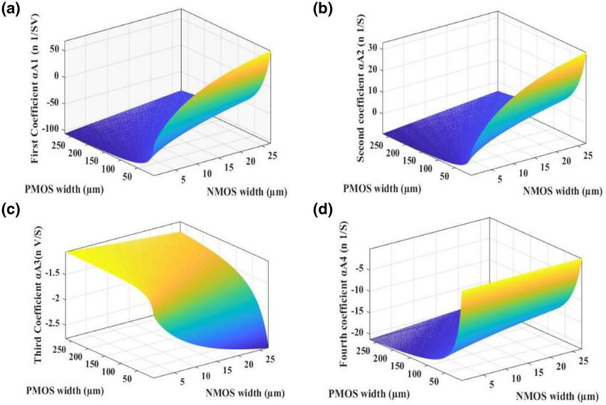
                                                                                                                                                                                                                                                                                                                                    performed and the variation of αA1–αA4 are computed and
                                                                                                                                                                                                                                                                                                                             ð11Þ   illustrated in Figure 7. As can be seen, all the coefficients are in
                                                                                                                                                                                                                                                                                                                                    the range of 10−9 with different dimensions. Except for αA3,
    Solving both Equations (10) and (11) for two variables,                                                                                                                                                                                                                                                                         the absolute values of all other ones are increased as the size of
Vm, and Vct, can be found. However, solving these two                                                                                                                                                                                                                                                                               PMOS increases. In the case of αA1 increasing the PMOS
strongly non‐linear equations simultaneously in terms of circuit                                                                                                                                                                                                                                                                    sized cause to sign change and change it from a positive value
parameters is very complicated and the results would not                                                                                                                                                                                                                                                                            to a negative one.
convey any useful qualitative information about the behaviour                                                                                                                                                                                                                                                                            Equation (2) models the variations of variable u from peak
of the output voltages. To overcome this problem, a compar-                                                                                                                                                                                                                                                                         value to the moment of jump upward, but in the proposed
ative study with reference [5] is made in the next section to                                                                                                                                                                                                                                                                       circuit a completely different process is followed to create the
show how a systematic model of pure mathematical environ-                                                                                                                                                                                                                                                                           equivalent of this portion of the signal.
ment could be implemented in the electronic word and its                                                                                                                                                                                                                                                                                 Referring to Figure 6, it is clear that, increasing Vct from
challenges.                                                                                                                                                                                                                                                                                                                         its minimum value until the beginning of the jump process
DALIRI   ET AL.
                                                                                                                                              -   181

FIGURE 7          Differential equation coefficients variations against NMOS (Mn1) and PMOS (Mp1) sizes. (a) αA1, (b) αA2, (c) αA3, (d) αA4

is done at a constant rate, which is dependent on the ratio                          In reality, two independent systems for one waveform are
of the excitation current to the equivalent capacitance of the                   impossible and surely, they will influence each other. As can be
node. Going down of Vct is also done by Mp3, which is                            seen in Table 2, B1–B4 are directly dependent on the size of
relatively faster than the variable u in Equation (2). Using                     NMOS and PMOS transistors. It shows that in each mathe-
interpolation techniques can certainly find a single function                    matical model the relation of these two parts should be
for modelling this part of the signal. Therefore, coefficient a                  clarified.
and b are not the main factors in determining the Vct                                Sharp jumping down could be obtained only in the WI
behaviour.                                                                       regime because of the exponential I‐V characteristic of tran-
                                                                                 sistors. This difference between polynomial approximation and
                                                                                 exponential relation is shown in Figure 6a. Polynomial
5 | DISCUSSION                                                                   approximation could model the rising part of waveform very
                                                                                 well but the second part of jumping down is not as precise as
Comparing circuit behaviour and mathematical models in                           exponential one. Due to power consumption limitation and
Equations (1)–(3), it becomes clear that there are some serious                  mimicking the biological system, using WI transistors are
challenges for implementing the mathematical equations in the                    inevitable. Using WI transistors cause the coefficients of the
electronics domain. These challenges have been attempted to                      differential equation to be in the nanoscale because they have a
be presented below in order to provide an overview, improving                    direct relationship with the size of the transistor. It shows that
the compatibility of mathematical models and implementation                      in spike dynamic modelling, the range of coefficients should be
criteria. Certainly, when implementation challenges are also                     considered.
taken into account, proposed models could be more applicable
and usable in circuit design.
     The model presented in reference [5] consists of two                        6 | CONCLUSION
completely separate and independent sections:
                                                                                 A comparative study between the circuit model and the
1. Spike initiation dynamics are modelled by two ordinary                        mathematical model of reference [5] is developed. To find a
   differential equations.                                                       more compatible mathematical neuron model with circuit
2. Auxiliary after spike resetting or jumping system in Equa-                    design, this paper provides the right conditions to be used as a
   tion (3).                                                                     reference for circuit design. For this purpose, a new topology
182
      -                                                                                                                                            DALIRI   ET AL.

for a differential AH artificial neuron is designed, which                        11. Hashimoto, S., Torikai, H.: A novel hybrid spiking neuron: bifurca‐tions,
doubles output spikes using fully differential structures. By                         responses, and on‐chip learning. IEEE Trans. Circuits Syst. I Reg. Papers.
                                                                                      57(8), 2168–2181 (Aug 2010)
comparing circuit behaviour and mathematical models, chal-
                                                                                  12. Gerstner, W., Kistler, W.M.: Spiking Neuron Models. Cambridge
lenges for implementing the mathematical equations in the                             University Press, Cambridge (2002)
electronics domain were addressed.                                                13. Zhang, L.: Building logistic spiking neuron models using analytical
                                                                                      approach. IEEE Access. 7, 80443–80452 (2019)
                                                                                  14. Abusnaina, A.A., Abdullah, R.: Spiking neuron models: a review. Int. J.
R EF ERE N CE S                                                                       Digi. Content Technol. Appl., 14–21 (Jun. 2014)
 1. Benjamin, B., et al.: Neurogrid: a mixed‐analog‐digital multichip system      15. Basu, A., Hasler, P.E.: Nullcline‐based design of a silicon neuron. IEEE
    for large‐scale neural simulations. Proc. IEEE. 102(5), 699–716 (May              Trans. Circ. Syst. I. 57(11), 2938–47 (2010)
    2014)                                                                         16. Joubert, A., et al.: Hardware spiking neurons design: analog or digital?
 2. Schemmel, J., et al.: A wafer‐scale neuromorphic hardware system for              2012 International Joint Conference on Neural Networks (IJCNN)
    large‐scale neural modeling. in Proc. IEEE Int. Symp. Circuits Syst.,             (2012)
    1947–1950 (May 2010)                                                          17. Cruz‐Albrecht, J.M., Yung, M.W., Srinivasa, N.: Energy‐efficient neuron,
 3. Merolla, P.A., et al.: A million spiking‐neuron integrated circuit with a         synapse and STDP integrated circuits. IEEE Trans. Biomed. Circuits
    scalable communication network and interface. Science. 345(6197),                 Syst. 6(3), 246–256 (2012)
    668–673 (2014)                                                                18. Indiveri, G., et al.: Neuromorphic silicon neuron circuits. Front Neurosci.
 4. Furber, S., et al.: The PiNNaker project. Proc. IEEE. 102(5), 652–665             5 (2011)
    (May 2014)                                                                    19. Mead, C.A.: Analog VLSI and Neural Systems. Addison‐Wesley. Reading,
 5. Izhikevich, E.M.: Simple model of spiking neurons. IEEE Trans. Neural             MA (1989)
    Netw. 14(6), 1569–1572 (Nov. 2003)                                            20. Galup, C., Schneider, M.: The compact all‐region MOSFET model:
 6. Zaghloul, K.A., Boahen, K.: A silicon retina that reproduces signals in           theory and applications. 2018 16th IEEE International New Circuits and
    the optic nerve. J. Neural Eng. 3(4), 257–267 (2006)                              Systems Conference (NEWCAS) (2018)
 7. Wen, B., Boahen, K.: A silicon cochlea with active coupling. IEEE Trans.
    Biomedical Circuits Syst. 3(6), 444–455 (2009)
 8. Sourikopoulos, I., et al.: A 4‐fJ/spike artificial neuron in 65 nm CMOS           How to cite this article: Daliri M, Ferreira PM,
    technology. Front Neurosci. 11(123), 1–14 (Mar 2017)                              Klisnick G, Benlarbi‐Delai A. A comparative study
 9. Danneville, F., et al.: A Sub‐35 pW Axon‐Hillock artificial neuron circuit.       between E‐neurons mathematical model and circuit
    Solid State Electron. 153, 88–92 (2019)
10. Ferreira, P.M., et al.: Energy efficient f J/spike LTS e‐Neuron using
                                                                                      model. IET Circuits Devices Syst. 2021;15:175–182.
    55‐nm node. Proc. ACM IEEE Symp. Integr. Circuits Syst. Design, 1–6               https://doi.org/10.1049/cds2.12017
    (Aug 2019)
You can also read