Introduction to Silicon Detectors - G.Villani STFC Rutherford Appleton Laboratory Particle Physics Department
←
→
Page content transcription
If your browser does not render page correctly, please read the page content below
Introduction to Silicon Detectors
                         G.Villani
           STFC Rutherford Appleton Laboratory
               Particle Physics Department

1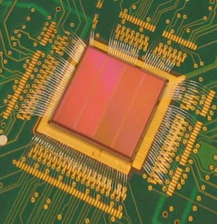
Outlook
    • Introduction to physics of Si and
      detection
    • Examples of detectors
    • Radiation effects and system issues
    • Conclusions

2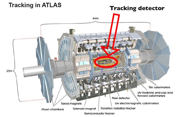
Introduction

                                                 The Si detection chain

              Sensing/        Charge transport                          Signal
    E       Charge creation    and collection
                                                      Conversion
                                                                      processing
                                                                                            Data TX

              Si physical                Si device properties         Si device topologies properties
              properties

                    all the boxes of the detection chain process based upon Silicon

        Detector physics:                          Detector examples:              Detector system issues:
        Silicon physical and electrical properties Strips, pixels                  Detection efficiency
        Detection principles                       MAPS                            Power
        Transport mechanisms                       ATLAS SCT
        Conversion

3
Silicon properties

                               After Oxygen, Silicon is the 2nd most abundant element
                               in Earth’s crust (>25% in mass)

                 The crystalline structure is diamond cubic (FCC), with lattice spacing of
                 5.43 A
                 •Polysilicon consists of small Si crystals randomly oriented; in α-Si there
                 is no long range order.
    Si
                 Apart from its abundance, that makes it also cheap, the key to success
                 of Si is related to its oxide SiO2, an excellent insulator (BV ~ 107 V/cm).
                 *Micro crystals but the flexible bond angles make SiO2 effectively an
                 amorphous: its conductivity varies considerably (charge transport in SiO2
         1.48A   via polaron hopping between non-bonding oxygen 2p orbitals)

4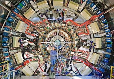
Silicon electrical properties
Silicon Band structure
The electronic band structure can be obtained by solving many-body SE in presence of periodic
potential of the crystal lattice: (normally 1 electron SE in periodic potential neglecting electron
interactions) : Bloch functions
(T + U )ψ = Eψ ⇒ ψ n,k (r ) = un,k (r )e jk⋅r En (k )
~ a wave associated with free motion of electrons modulated by the periodic solution un,k. The energy
E is periodic in k so is specified just within the 1st unit WS cell of the reciprocal lattice (the Brillouin
zone).
èThe appearance of Band Gap, separating CB
VB and VB
èThe 6 CB minima are not located at the center
CB
of 1st Brillouin zone, INDIRECT GAP
1st Brillouin zone of Diamond lattice
5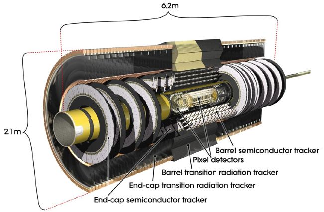
Silicon electrical properties
The detailed band structure is complicated: usually quasi-equilibrium simplifications
are sufficient to study the charge transport.
Assuming that the carriers reside near an extremum, the dispersion relationship
E(k) is almost parabolic:
2 * 3/ 2
E (k ) =
2 k
→ g (E ) =
(2m )
0
E − Eo
2m0* 2 3
2π
2
2 k 1 k 〈 p〉
E (k ) = *
→ v = ∇ k E (k ) = * = *
2m0 m0 m0
dk (t ) d 〈 p〉
= = − ∇ rV ≅ F
dt dt
èUnder the assumptions of small variation of the electric field, the carrier dynamics
resembles that one of a free particle, with appropriate simplifications.
èThe effective mass approximation takes into account the periodic potential of the
crystal by introducing an effective carrier mass ( averaged over different longitudinal
and transverse masses) . The lower the mass, the higher mobility (µ ∝ 1/m*)
A similar approach is used to calculate the E(k)
for phonons.
6
Silicon electrical properties
The carrier density is calculated from:
CB • The density of states g(E), which depends on dimension;
• The distribution function F(E);
Only partly filled bands can contribute to conduction: carrier
density in CB and VB.
VB At equilibrium the carrier density is obtained by integrating
the product:
nD = ∫ g D (E )F (E )dE ≅ N C /V e − ( Ec − Ev )/ kT = ni = pi
3
1
F (E ) =
⎛ E − EF ⎞
1 + exp⎜ ⎟
2 ⎝ kT ⎠
2 ( )
− E g / kT 20
pn = ni = N C N V e ≅10 @ T = 300K
1
*Fermi level: energy level @ 50% occupancy
In intrinsic Si a creation of e in CB leaves behind a hole in VB,
0 that can be treated as an e with positive charge and mobility of
the band where it resides
The density of states gD(E) depends on the dimension
7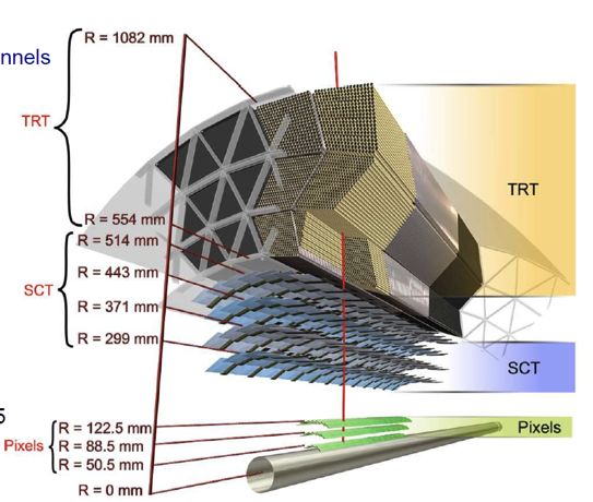
Silicon electrical properties
èConduction of Si intrinsic @ T = 300K:
σ = q(µn +µp) ni = 3.04x10⁻⁶mho-cm ->329kOhm-cm
èBy adding atoms of dopants, which require little
energy to ionize ( ~10’s mEV, so thermal energies @
ambient temperature are enough) we can change by
many orders of magnitude the carrier concentration.
èDoping concentration: 1012 to 1018 cm-3
In crystalline Si ~ 5*1022 atoms cm-3
In equilibrium and for non degenerate case
the relationship between carrier concentration and E
is the same as in the intrinsic case:
( )
− E g / kT
pn = ni2 = N C NV e ≅ 1020 @ T = 300 K
ni2
e.g. : N D = 1017 ⇒ pn ≅ pN D → p ≅ = 103
ND
8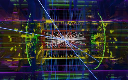
Detection principles
       Detection principles:

       A: Ionization: by imparting energy to break a bond, electrons are lifted from VB to CB then
       made available to conduction. Most exploited concept ( ionization chambers, microstrip, hybrid
       pixels, CCD, MAPS…)

       B: Excitation: Charge or lattice (acoustic or optical phonons) some IR detectors, bolometer
                                                                   α

                            MIP

                                                                         Photon interaction   I ( z ) = I o e −α ( E ) z

    Bethe-Bloch formula for stopping power gives the rate of energy loss/unit
    length for charged particles through matter

9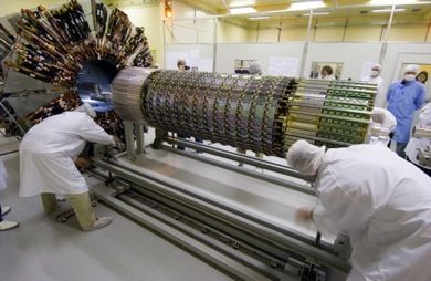
Detection
Ph: ΔQ~107 m-1
ΔQ~1010 m-1
π/a
The indirect BG semiconductors require higher energy than naively expected from their band
gap for charge excitation, because energy and momentum must be conserved (Phonon-
assisted pair creation/recombination)
è In Si an average of 3.6 eV is required for pair creation
10Detection
MIP charge density Photoelectric charge density
dE 1 1 I ( z ) = I o e −α ( E ) z
n= ρ 2
≅ 3 ⋅1015 cm −3
dx ε i π ⋅ R
γ ⋅v P −α (λ ) z
R= ≅ 110nm n ( z ) = in ηα (λ )e ≅ 5.6 ⋅10 6 e − / µm
I λ hν
A MIP forms an ionization trail of radius R
An optical power of -60dBm (= 1nW) of 1keV
when traversing Si, creating ~ 80e-/µm
photons generates ~ 6*106e-/μm
èHigh injection regime:
h Plasma effects
λ≅Detection
The variance in signal charge σi associated to the ionization process is related to the phonon excitation
Eo E pn ⎛ ε i ⎞
σi = ⎜⎜ − 1⎟⎟
εi Ei ⎝ Ei ⎠
Fano factor ~0.1 in Si
High resolution requires smaller band gap (εi ),
direct or small phonon excitation energy
Intrinsic resolution of Si and Ge based detectors
12Detection
B: Excitation:
60meV
Poly Si SiO2 Si
Ec
EF
~10’s meV
EV EF
Eigenvalues separation in quantized structures ~ 10’s meV
Dispersion relation for phonons in Si
Phonon excitation energy ~ 10 meV : much lower threshold
13Charge transport
Charge transport:
Once the charge has been created in the material, the next step is its collection:
The charge transport description relies on semi-classical BTE (continuity equation in 6D
phase space)
( )
∂f r , k , t 1 F
+ ∇ k E (k )⋅ ∇ r f (r , k , t ) + ⋅ ∇ k f (r , k , t ) =
(
∂f r , k , t ) + S (r , k , t )
∂t ∂t coll
1
( )
n r, t =
V ∫ f (r , k , t ) Q conservation
k
q
( )
J r, t = −
V ∫k
v(k ) f (r , k , t ) P conservation
1
( )
W r, t =
V ∫k
E (k ) f (r , k , t ) E conservation
14Charge transport
Under (many) simplifying assumptions the 1st moment of BTE gives the DD model
(The ‘semiconductor equations’):
Drift term
J n = qnµ n E (r ) + qDn∇n Diffusion term
J p = qpµ p E (r ) − qD p ∇p
∂n 1
= ∇ ⋅ Jn +Un
∂t q
∂p 1
= − ∇ ⋅ J p +U p
∂t q
∇ ⋅ ε∇V = −( p − n + N D+ − N A− )
èDD expresses momentum conservation: it becomes invalid when sharp variation in energy
of carriers occur (due to F for example: deep submicron devices)
When feature size is 0.’sµm the DD model becomes invalid: higher moments required
15Half summary
Under a number of assumptions, the description of the detection processes in semiconductor detectors
can be hugely simplified:
Sensing/ Charge transport
E Charge creation and collection
Conversion
Si physical Si device properties
properties
Physical characteristics: Charge generation: Charge transport:
Quasi equilibrium; Ionization: Small Big devices, DD
injection, QM not adequate;
Homogeneity;
needed;
Small injection, electric
‘Room’ temperature;
Stopping power, field as static;
Non degenerate Si; average ionization
energy
Under conditions of
• quasi stationary conditions
• non degenerate semiconductor
• not small feature size
• low injection
•…
16Detectors examples
Strip / pixel detectors
HEP, Scientific applications
PN junction
Monolithic Active Pixel Sensors (MAPS)
Consumer and scientific applications
Charge Coupled Devices (CCD)
Imaging, scientific and consumer applications
RAL PPD has (is) actively involved with all these detector technologies
17Detectors examples
Use of Si detectors
èAlmost all HEP experiments use Si detectors:
The high density track region usually covered by pixel detectors; by strip
at larger radius (cost reason)
18Signal conversion: The PN junction
Homojunction: two pieces of same semiconductor materials
with different doping levels:
• In equilibrium, the Fermi level equalizes throughout the structure
• thermal diffusion of charge across the junction leaves a depleted
region, with the ionized dopants : an electric potential Φ, and a field
F F, develops across
• the charge concentration depends exponentially on energy, or Φ:
Δϕ
Vt
0 = qnµ n E (r ) + qDn∇n → n = n0e
ϕ =0 In equilibrium J = 0 −
Δϕ
Vt
0 = qpµ p E (r ) − qD p∇p → p = p0e
• by applying a small voltage to decrease the barrier, the charge
increases exponentially
• by applying a voltage to increase the barrier, the depleted region
increases
èUnidirectionality of current characteristics
19Signal conversion: The PN junction
• when charge is generated in the depleted region is swept
across by the electric field sustained by the ionized dopants
and the biasing.
è PN junction as signal converter: capacitor with a F across
è A PN junction with a large depleted region can be used to
efficiently collect radiation generated charge (Solid state
ionization chamber)
W
2εVb N a + N d
Depletion width W=
q Na ⋅ Nd
To achieve large W high field region:
• Low doping (high resistivity),Na or Nd
• Large voltages Vb
20Detectors examples
Strip detectors
Pitch 10’s μm
≈ 300μm
(high res)
F
Q transversal diffusion RO
Vbias ~100’sV
Array of long silicon diodes on a high resistivity silicon substrate
A strong F in the high resistivity Si region helps collect charge efficiently.
è The high resistivity Si is not usually used in mainstream semiconductor industry:
Hybrid solution: sensor (high resistivity Si) connected (wire/bump-bonded) to the readout
electronic (low resistivity Si)
21Detectors examples
ATLAS SCT RO ASIC (ABCD3TA)
12 RO ASIC 128 channels/ASIC
768 Strip Sensors
RAD-HARD DMILL technology
ASICS glued to hybrid
40 MHz Ck
ATLAS SCT
4 single-sided p-on-n sensors
2x2 sensors daisy chained
Stereo angle 40 mrad
Strip pitch 80 µm
768 channels/side
Binary RO
Bias Voltage up to 500 V
Operating temperature -2 C
Space point resolution: rPhi 17µm / z 50 µm
Power consumption: 5.6 W (initially ) to 10 W ( after 10y)
Rad hard up to 2x10¹⁴ 1-MeV n eqv/cm2
22Detectors examples
ATLAS SCT
61 m2 of Si
6.3 * 106 channels
50 kW total power consumption
1 barrel
- 4 layers
- 2100 modules
2 endcaps
- 9 disks/each
- 988 modules
2 T solenoidal field
23Detectors examples
ATLAS Tracker overview
Pixel: (n+ on n) 1.8m2, 80M channels
SCT: 61 m2 6.3Mchannels
TRT: 0.4M channels
24Detectors examples
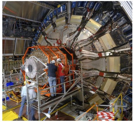
Barrel insertion in the ATLAS Cavern
ATLAS SCT - Red cables : power cables
25Detectors examples 26
Detectors in operation

               An ATLAS event with 4 muons. The four muons are picked out
               as long blue tracks.

27
Detectors in operation 28
Detectors examples
MAPS detectors ≈1’s µm
RO electronic
RO electronic
3T ( 3MOS) MAPS structure
2 D array of pixels
è Monolithic solution: detector and readout
integrated onto the same substrate
29Detectors examples
MAPS detectors
Vbias ~V’s
N++ (low res)
Electronics
0.’s µm
Active region P+ (low-med res)
‘s µm
P++ (low res)
Mechanical substrate
100’s µm
è The charge generated in the thin active region moves mainly by diffusion :
‘Long’ collection time
Small signal
Low radiation hardness
èHowever, complex circuit topologies allow DSP on pixels for low noise performances (≈ some e-
noise)
30Detectors examples
Example of MAPS detectors:
10-7
TPAC 1 pixel size 50x50 µm2
Chip size ~1cm2
Total pixels 28k
>8Meg Transistors
∂n 2 l2
≅ Dn∇ n + U n → tcoll ≅
∂t Dn
Charge collection time (s) in MAPS vs. perpendicular MIP hit
31Detectors examples
Example of charge collection in MAPS: simulated MIP vs.1064nm laser 2x2 µm2 5ns pulse
32Detectors example
Proposed use of MAPS (50x50 µm2) sensors in SuperB Vertex Tracker
33Radiation damage
In HEP and space applications the detectors are exposed to high level of dose of radiation:
LHC: 10’s Mrad (100kGy) over 10 years of operation
N.B.: 1 rad/cm3 Si ~1013e/h pairs
Lethal dose: 5 Gy Total Body Irradiation
34Radiation damage
Radiation environment in LHC experiment
TID Fluence
1MeV n eq. [cm-2] @ 10 years
ATLAS Pixels 50 Mrad 1.5 x 10¹⁵
ATLAS Strips 7.9 Mrad 2 x 10¹⁴
CMS Pixels ~24Mrad ~6 x 10¹⁴ *
CMS Strips 7.5Mrad 1.6 x 10¹⁴
ALICE Pixel 250krad 3 x 10¹²
LHCb VELO - 1.3 x 10¹⁴/year**
All values including safety factors.
35Radiation damage
Microscopic effects: Bulk damage to Silicon : Vacancy
Displacement of lattice atoms V
+
EK>25 eV
I Interstitial
èAtoms scattered by incoming energetic particles leave behind vacancies or atoms in
interstitial positions (Frenkel pairs).
Low energy particle ~ point defects
High energy particles ~ cluster defects
36Radiation damage
altered Band gap Altered
Energy Atoms
Lattice Spurious Electrical
deposition displacement
periodicity states characteristics
generation recombination
trapping Conduction band
Donor levels +++
compensation
-
Band gap
Acceptor levels
Valence band
èThe appearance of spurious band gap states affects the electro/optical characteristics of the device:
• Thermal generation of carriers (increased leakage current)
• Reduced recombination time ( quicker charge loss , reduced signal)
• Charge trapping
• Scattering
• Type conversion
37Radiation damage
Macroscopic effects:
Charge Collection Efficiency (CCE) is reduced by decreased recombination time and trapping
Noise increases because of increased leakage current
Depletion voltage increases because of type inversion ⎛ 1 ⎞
Qe,h (t ) = Q0 e,h exp⎜ − ⋅ t ⎟
⎜ τ ⎟
⎝ eff e,h ⎠
1015 1MeV n-eq.
1
∝ N defects
τ eff e,h
38Radiation damage
To increase the Radiation Hardness of Sensors:
• Operating conditions (cooler – lower leakage)
• Material engineering ( OFZ - Diamond detectors)
• Device engineering (n in n/p – 3D detectors):
• Electrodes in the bulk – lateral collection reduces the
drift distance
• Lower depletion voltage – less power consumption
• difficult to manufacture
•3D DDTC similar to 3D but easier to manufacture; also
Better mechanical strength.
n+
F
p+
39Detector systems
èHEP experiments: large detector systems
Challenging engineering issues Alternative powering schemes:
SP
DC2DC
A serial powering (SP) or DC2DC approach can increase
The ATLAS SCT (semiconductor tracker) detector.
efficiency in power distribution compared to a parallel approach
The thick red cables on show feed the detector with half of its
power
Low power solutions are crucial for future HEP ( and others) experiments:
Estimated lowest power consumption for simple generic pixel: ≈10 µW
10µW continuous -> 10µJ energy
Energy deposited by a MIP particle: 0.2 – 10fJ
Required energy/deposited energy >> 1010 !!!
‘Huge’ energy inefficiency
40Conclusions The field of semiconductor detectors encompasses different scientific and technology fields: solid state physics, nuclear and particle physics, electrical engineering, … Some of the issues relevant to particle and radiation detectors: • Development of new detection techniques based on novel and well established semiconductor material: ( phonon-based detectors, quantum detectors, compounds, low dimensional) • Integration with electronics (monolithic solution to achieve more compactness and reduce cost) , 3D structures • Topologies optimization (power reduction, noise reduction) • Simulation and modelling; • Radiation hardness 41
You can also read