Alligator clips to molecular dimensions - Nicholas Prokopuk1 and Kyung-Ah Son2
←
→
Page content transcription
If your browser does not render page correctly, please read the page content below
IOP PUBLISHING                                                                                    JOURNAL OF PHYSICS: CONDENSED MATTER
J. Phys.: Condens. Matter 20 (2008) 374116 (21pp)                                                    doi:10.1088/0953-8984/20/37/374116

Alligator clips to molecular dimensions
Nicholas Prokopuk1 and Kyung-Ah Son2
1
    NAVAIR Research Department, Chemistry Branch, China Lake, CA 93555-6100, USA
2
    Jet Propulsion Laboratory, Pasadena, CA 91109, USA

Received 13 May 2008
Published 26 August 2008
Online at stacks.iop.org/JPhysCM/20/374116

Abstract
Techniques for fabricating nanospaced electrodes suitable for studying electron tunneling
through metal–molecule–metal junctions are described. In one approach, top contacts are
deposited/placed on a self-assembled monolayer or Langmuir–Blodgett film resting on a
conducting substrate, the bottom contact. The molecular component serves as a permanent
spacer that controls and limits the electrode separations. The top contact can be a thermally
deposited metal film, liquid mercury drop, scanning probe tip, metallic wire or particle.
Introduction of the top contact can greatly affect the electrical conductance of the intervening
molecular film by chemical reaction, exerting pressure, or simply migrating through the organic
layer. Alternatively, vacant nanogaps can be fabricated and the molecular component
subsequently inserted. Strategies for constructing vacant nanogaps include mechanical break
junction, electromigration, shadow mask lithography, focused ion beam deposition, chemical
and electrochemical plating techniques, electron-beam lithography, and molecular and atomic
rulers. The size of the nanogaps must be small enough to allow the molecule to connect both
leads and large enough to keep the molecules in a relaxed and undistorted state. A significant
advantage of using vacant nanogaps in the construction of metal–molecule–metal devices is that
the junction can be characterized with and without the molecule in place. Any electrical
artifacts introduced by the electrode fabrication process are more easily deconvoluted from the
intrinsic properties of the molecule.
(Some figures in this article are in colour only in the electronic version)

1. Introduction                                                       vinylene), the organic molecules must be connected between
                                                                      electrical leads that interface the macroscopic dimensions.
As electronic circuits approach sub 50 nm dimensions, the             More complex circuits comprising hundreds or thousands
size constraints, fabrication cost, and physics of conventional       of molecular switches with the necessary interconnections
silicon chips face severe technological challenges [1].               between the nanodevices and external connections to input
Consequently, new materials with the desired electronic               and output leads pose even greater challenges to the field
properties and functionality are being pursued to construct           of molecular electronics. Reed and Tour [5] demonstrated
memory devices and logic circuits with dimensions on the              one of the first experimental measurements of a molecule’s
order of a few nanometers. Since Aviram and Ratner                    conductivity by constructing metal–molecule–metal junctions
first postulated that the electronic properties of a molecular
                                                                      from a mechanical break in a gold wire.             Although
dipole can mimic that of a diode [2], the field of molecular
                                                                      the mechanical break junctions are not easily incorporated
electronics was born and the prospects of constructing
                                                                      into more complex circuitry, they demonstrated that metal
transistors, switches, and resistors from molecules promised
                                                                      electrodes could be generated with the nanometer separations
an alternative to silicon based technologies with nanometer-
sized components [3, 4]. However, interfacing the molecular           necessary to bridge molecular circuits to macroscopic
nanostructures into integrated circuits requires controlled           leads. Subsequently, several approaches to generating metal–
placement of electrical contacts with subnanometer resolution.        molecule–metal devices have been developed for probing the
Reliably configuring metal electrodes with the necessary              electronic properties of organic elements and constructing
separations capable of linking nanometer-sized component              arrays of molecular junctions in complex circuits.
remains a major obstacle to generating molecular circuits.                 Careful manipulation and fabrication of metal electrodes
      In order to simply compare the electrical properties of         with well-defined separations that are on the order of a few
a saturated alkyl chain and a conjugated oligo(phenylene              nanometers is possible with varying degrees of complexity.

0953-8984/08/374116+21$30.00                                      1                          © 2008 IOP Publishing Ltd Printed in the UK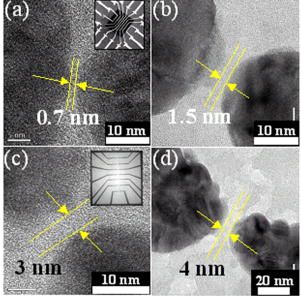
J. Phys.: Condens. Matter 20 (2008) 374116                                                                        N Prokopuk and K-A Son

Nanojunctions have been formed using electromigration                  the footprint of a single molecule. Consequently, the process
techniques [6], electrochemistry [7], nanolithography [8],             used to establish the top contact dictates the overall dimen-
scanning probes [9], break junctions [5], and crossed                  sions of the device. Lithographically patterned top contacts are
wires [10]. Levels of sophistication range from the surprisingly       convenient for constructing large integrated arrays of molec-
simple mercury drop contacts [11] that utilize nothing more            ular circuits with cross-sectional areas that are significantly
than ordinary lab equipment to make a top contact to a self-           larger than the dimensions of the molecular elements. By con-
assembled monolayer (SAM) on a metal film to more intricate            trast, scanning probes on SAMs can reduce the footprint of the
scanning probe and electron-beam lithographic techniques that          molecular junction to a single molecule. However, probe tech-
require dedicated instrumentation worth hundreds of thousands          niques are ill suited for constructing integrated circuits com-
or millions of dollars [12]. Despite these great differences,          prising hundreds or thousands of devices. Metal–molecule–
the various strategies for generating metal–molecule–metal             metal devices constructed with large top contacts contain mul-
junctions can be categorized into two basic approaches. In             tiple molecules in parallel within each junction. Significant
the first, a top-contact is made to a molecular film deposited         differences between the collective properties of these ensem-
on a conducting substrate. The second strategy involves                bles and the tunneling properties of a single-molecule junction
fabricating vacant nanogaps and subsequently inserting a               can contribute to unexpected conductance values. As a result,
molecular element between the nanospaced electrodes. There             the normalized conductance of molecular resistors varies with
are a number of variations within the two approaches and               the size and type of the top contact [15]. Moreover, devices
each unique process for connecting a molecule between two              with large footprints greatly increase the dimension of the cir-
electrodes entails its own set of advantages and disadvantages.        cuit element beyond the few square nanometers promised by a
The goal of this review is to highlight the different approaches
                                                                       single-molecule transistor.
for constructing nanojunctions suitable for studying electron
                                                                            Importantly, the method used to establish the top contact
tunneling in metal–molecule–metal devices.
                                                                       can have a dramatic effect on the organic layer and introduce
                                                                       electrical artifacts that are difficult to differentiate from
2. Top-contact junctions                                               the intrinsic properties of the molecule. The absence of
                                                                       obvious control experiments, such as obtaining the electric
In the top-contact method, a SAM or Langmuir–Blodgett
                                                                       response of the junction in the absence of the molecule
(LB) film containing the specific molecular component with
                                                                       or measuring the molecule’s conductance without the metal
the desired electrical properties is initially deposited on a
                                                                       contacts, further convolutes the resistivity of the molecule
conducting substrate. The interface between the substrate and
                                                                       with the effects of the top contact.            Once the top
SAM or LB film serves as one metal–molecule connection
                                                                       contact is in place, the spectroscopic tools available for
(bottom contact). A top contact is then made to the top
                                                                       characterizing the intervening molecule are greatly limited
or exposed surface of the organic film. The two contacts
                                                                       by the metallic properties of the metal electrodes which
connect the molecules in the SAM or LB film to external
                                                                       prevent the transmission of vibrational spectra. Inelastic
circuits. Several strategies for making the top contact have
been reported including conventional scanning probes [9],              tunneling spectroscopy can provide low-temperature structural
thermally deposited metal layers [13], mercury drops [11],             information on the molecular junction [16]. Knowledge of
metal colloids [14], and crossed-wire junctions [10]. The              the structure and function relationship of the organic film
key advantage of the top-contact approach is that the SAM              is important in identifying the mechanisms responsible for
and LB films containing the molecular component sets the               switching a molecule’s resistance between conducting and
electrode spacings at the precise distance needed to connect           nonconducting states. This is all the more important if the
the two ends of the molecule. In effect the molecular element          electronic properties of the metal–molecule–metal junction
acts as both circuit element and template for controlling the          are to be controlled by chemical changes in the molecular
metal–metal separation. Top-contact metal–molecule–metal               component.
connections are possible regardless of the molecule’s length or
thickness as long as the molecule is within a stable and robust        2.1. Scanning probes
SAM or LB film that prevents shorting when the top contact is
added. One benefit of employing the top-contact method is that         Scanning tunneling microscopy (STM) provided some of the
asymmetric molecules can be uniformly aligned normal to the            earliest attempts to connect macroscopic leads to molecular
surface to investigate the directional tunneling properties of a       circuits [17, 18]. STM and the more recently developed
molecular dipole. The flexibility in the types of molecules that       technique of conducting atomic force microscopy (c-AFM)
can be assembled into SAMs and LB films, control over their            operate on similar principles: a metallic tip is brought into
orientation within the film, and the straightforward methods for       close proximity to a conducting substrate and a bias is placed
adding a top contact make the top-contact approach extremely           between the tip and substrate [19]. Current flowing between
versatile for investigating charge transport through a diverse         the tip and surface is used to quantify the resistivity of
range of structures.                                                   molecules immobilized on the substrate. The advent of
     The length of metal–molecule–metal junctions con-                 scanning tunneling spectroscopy (STS), which monitors the
structed from the top-contact method is typically on the or-           change in current as a function of potential, allowed resistivity
der of a single-molecule layer or bilayer. However, the cross-         data of a molecular film to be obtained with subnanometer
sectional area of the metal leads are typically much larger than       spatial resolution [20]. One of the early uses of STS

                                                                   2
J. Phys.: Condens. Matter 20 (2008) 374116 N Prokopuk and K-A Son
on self-assembled monolayers adsorbed to gold substrates
demonstrated the rectification behavior of easily polarized
oligo(phenylene ethynylene) structure and, thus, confirmed
Aviram and Ratner’s prediction [21].
The spatial resolution of the scanning probes is well
suited for accessing arrays of molecular on/off switches for
memory storage. In this application, a molecular memory
unit is toggled between high and low conductive states with
a unipolar pulse. Individual molecules with cross-sectional
areas of a few nanometers are easily distinguished from
an insulating background [22]. Thus, the memory unit is
reduced to the dimensions of the molecular element and
the insulating (nonconducting) surrounding. Unfortunately,
metal–molecule–metal junctions formed with top contacts
made with a scanning probe lack the interconnectivity
necessary for logic operations and are not readily adaptable
for working collectively in tandem due to the piezoelectric
translational mechanism used to move the contacting tips.
In conventional STM experiments on SAMs bound to
gold surfaces, the metal tip is separated by some distance
from the molecular layer. A tunneling current flows via
overlap of the wavefunctions of the tip and molecule with an
applied bias. The tip–molecule distance can fluctuate over
the timescale of the STS or STM experiment. Due to the
exponential dependence of the tunneling current on distance,
a small deflection in the tip height significantly affects the
electric current. However, over shorter time periods, the
tip–molecule separation can be considered constant allowing
I –V measurements on a relatively static metal–molecule–
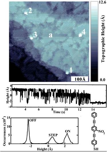
metal junction. The presence of a gap between the tip and Figure 1. STM topological map of a gold surface (top) modified
molecule introduces an additional resistive element that must with the nitro-oligo(phenylene ethynylene) in a host dodecanethiol
be deconvoluted from the electrical measurements in order to monolayer. The real-time height versus time plot (middle) indicates a
switching of the height of the oligomer. The occurrence versus height
extract the molecule’s conductance [23]. Mechanical contact plot (bottom) indicates ON, OFF, and STEP states [32]. Reprinted
between the tip and molecule can minimize the top contact- with permission from [32]. Copyright 2007 American Chemical
molecule resistance. However, care must be taken to limit Society.
tip-induced deformations in the molecular film such as bends
or conformational changes which can dramatically affect the to control the preferred conformation by altering the chemi-
tunneling resistances by several orders of magnitude [24, 25]. cal environment surrounding the oligomer [33]. Insights into
With a combination of current–voltage and current– a molecule’s electrical properties can still be acquired with
distance measurements, c-AFM, STM and STS can yield conventional scanning probe microscopy and spectroscopy de-
relative barrier heights [26–28], negative differential resis- spite the presence of a gap resistance between the probe tip and
tance [29, 30], phase differences [31], stochastic conductiv- molecular element.
ity switching [22, 32, 33], redox-activated switching [34], The distance between the probe tip and the molecular
photo-induced resonant tunneling [35], supramolecular cou- film can be effectively reduced to zero by forming a
pling [36], and conformational changes [37, 38] in a variety of covalent attachment between the SAM and the metal
molecular structures self-assembled on gold surfaces. In one tip. In this approach a symmetric bisthiol such as 1,6-
set of experiments, Tour’s group utilized a 10 kHz data collec- hexanedithiol extends from a gold substrate to a c-AFM or
tion with a fixed lateral position to monitor the conductivity of STM tip. The distill thiol attaches to the tip creating a
oligo(phenylene ethynylene) and related molecules as a func- covalent metal–molecule–metal junctions which lacks the gap
tion of time [32, 33, 37, 38]. Surprisingly, they found that the resistance between the top of the SAM and the probe tip.
apparent height of the oligomers varied stochastically between With the symmetric linkage, the metal–molecule interfacial
two values under constant current conditions, figure 1. These resistances are more easily identified from the current–distance
observations were ascribed to changes in the electronic struc- profiles [39]. However, in this close proximity to the
ture of the oligomer–metal interactions resulting from oscilla- surface, the probe tip is susceptible to covalent attachment to
tions in the molecule’s binding to the surface. As the molecule multiple molecules within the SAM layer. Single-molecule
fluctuates between two binding modes, the barrier height of the conductivities can be obtained by pulling the probe tip away
junction changes resulting in apparent increases or decreases from the surface and systematically breaking the covalent
in height (on/off states). Furthermore, Tour’s group was able linkages to the thiols [9, 25, 40–43]. As each organothiol
3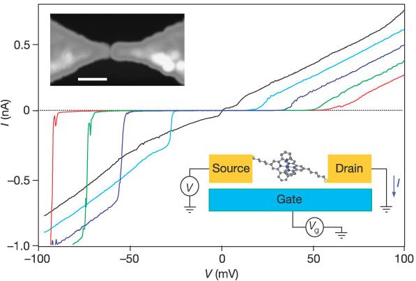
J. Phys.: Condens. Matter 20 (2008) 374116                                                                          N Prokopuk and K-A Son

                                                                         2.2. Permanent top contacts
                                                                         Integrated circuits of metal–molecule–metal junctions require
                                                                         robust electrode geometries that can be deposited or printed
                                                                         over large areas. Thermal deposition or contact printing of a
                                                                         top electrode on a SAM or LB film yields physically stable
                                                                         molecular circuits using simple lithography to pattern the
                                                                         electrodes. Top contacts in metal–molecule–metal junctions
                                                                         formed from deposited metal layers are not easily removed
                                                                         without destroying the circuit. While the size of these devices
                                                                         is not significantly improved over silicon based circuits, they
                                                                         demonstrate that molecular elements can be incorporated into
                                                                         working circuits that interface with external electronics. A
                                                                         significant benefit of these permanent top-contact junctions
                                                                         is that the lithography used to pattern the metal electrodes
                                                                         can also construct interconnects that join the molecular
                                                                         junctions to each other and to external circuits on macroscopic
                                                                         dimensions. For example, crossbar networks formed from
                                                                         orthogonal arrays of metal wires sandwiching molecular
                                                                         switches have been prepared and successfully demonstrated
                                                                         logic functions and memory storage [45, 46]. Junctions
                                                                         composed of 40 nm wide wires and cross-sectional areas of
                                                                         1600 nm2 containing approximately 1100 molecules each [47].
                                                                         Crossbar arrays have been prepared with device yields of
Figure 2. Histogram of conductance values (top left) obtained from       85% and a nonvolatile memory density of 6.4 Gb cm−2 .
metal–molecule–metal junctions formed with scanning probes on            While the mechanism responsible for conductivity switching
SAMs of 1,4-diaminobenzene (1) and 2,7-diaminofluorene (2) and
conductance traces obtained by raising the probe tip away from the       in these circuits is uncertain, the lithographically produced
surface [9]. Reproduced with permission from [9]. Copyright 2006         architectures demonstrate that functional electronics can be
Wiley-VCH Verlag GmbH & Co.                                              constructed from metal–molecule–metal circuits on a large
                                                                         scale.
disconnects from the surface or the tip, a covalent pathway                   A significant portion of the work on metal–molecule–
for electron tunneling is broken and the conductivity of the             metal junctions with permanent top contacts has been
junction drops. Since each thiol provides nearly the same                performed using thermally deposited metal leads. Studies on
resistance, the drop in current is stepwise and each drop in             the interactions of organic SAMs and LB films and metal
conductance corresponds to that of a single bridging bisthiol.           vapor such as that from thermally deposited titanium/gold
By repeatedly forming and breaking contact between the                   contacts indicate that the metal–molecule interface is not
probe tip and the surface-bound molecule, histograms of the              necessarily discrete. Specifically, interfacial reactions between
organic film’s conductance can be obtained with peak values,             the depositing metal film and the organic layer can introduce
figure 2. It should be noted that each drop in current is not            new chemical species with unknown electronic states. For
in perfect unity since the resistance of individual molecules            example, titanium patterned on alkyl layers results in metal
changes as the organothiol’s geometry deforms during the                 carbide formation [48, 49].          By contrast naphthalenes
stretching process. Interestingly, just prior to breaking a metal-       remain undamaged after titanium deposition keeping the
thiol connection, the conductance of the bridging alkyl chain            molecule’s electronic properties intact [50]. Extensive studies
increases. This small improvement in the alkyl’s resistance              on the effect of the head group of the organic film on
is attributed to changes in the confirmation of the chain                the reactivity of the SAM with vapor phase metal reveal
from gauche to the all-trans configuration [42]. Kushmerick              that monolayer degradation can occur by several different
and Bazan compared the conductivities of thiol-terminated                mechanisms [51, 52]. The electronic properties of metal
oligo(phenylene vinylene)s obtained with conventional STM                carbides within the gaps can dominate the energetics and
and contact-AFM [44]. In these experiments the coordination              charge transport properties of the metal–molecule–metal
of a single thiol to the gold surface in the asymmetric junctions        junctions and override any contributions of the molecular
of a non-contacted STM splits the low-lying molecular orbitals           complex. Importantly, the integrity of the organic film should
of one half of the organic fragment. In contrast the symmetric           not be assumed to remain intact as the deposition of the top
metal–molecule–metal junction formed with the c-AFM and                  contacts may introduce electronic artifacts into the nanogap
the bisthiols results in an even distribution of the molecular           and alter the chemical composition of the junction.
orbitals through the entire molecule and a higher conductance.                Despite complications arising from chemical reactions
The perturbation of the molecule’s orbitals by the sulfur’s              between the metal leads and the organic film, viable circuits
bonding to the surface suggests that the linking mechanism               have been fabricated with thermally deposited top contacts
between the molecular circuits and the electrical leads can              on redox active films of rotaxanes and catenanes. Metal–
greatly influence the device performance.                                molecule–metal junctions composed of these supramolecular

                                                                     4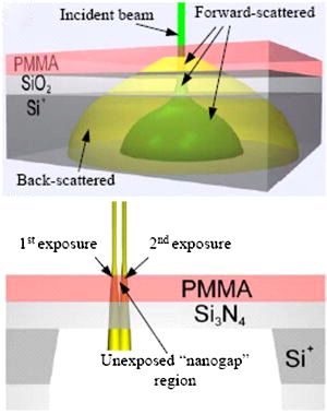
J. Phys.: Condens. Matter 20 (2008) 374116                                                                           N Prokopuk and K-A Son

complexes sandwiched between thermally deposited gold                    the underlying substrate. The cross section of the molecular
electrodes exhibit large hysteresis in their I –V curves [45, 46].       junctions and the available area for metal vapor to penetrate can
The conducting and nonconducting states of the rotaxanes and             be reduced with a nanopore to house the organic SAM [63–65].
catenane are sufficiently different that they can be assigned            This strategy reduces both the size of the molecular junction
binary values. The unipolar voltage-switching of the junction’s          and the possibility of deleterious interactions between the
resistance was initially attributed to changes in the oxidation          metal vapor and organic phase.
state of the molecules and any concomitant structural changes                  Metal–molecule–metal junctions fabricated with the top-
caused by the redox process. Subsequent studies on thermally             contact method require the effects of the top contact to be
deposited top-contact metal–molecule–metal devices revealed              considered when interpreting the electrical response of the
that the conductance switching is independent of the type of             device. Despite the successful construction of integrated
molecule in the junction. For example, metal–molecule–metal              circuits that demonstrate logic functions using molecular
junctions fabricated from LB films of fatty acids exhibit similar        switches and thermally deposited or printed leads, the structure
conductance switching properties as those constructed with the           and function of the molecular component and its role in
more complex rotaxane molecules despite lacking the redox                the conductance switching mechanism is not clear. By
activity of the rotaxanes [53]. Consequently, the mechanism              employing different methods for introducing the top contact,
for effectively toggling the resistivity of the rotaxane and             the conductivity of molecular resistors can be studied in
alkyl chain is most likely not molecular in nature. Rather,              a variety of configurations and testbeds. A combination
metal ion motion from the metal electrodes and filament                  of scanning probes, crossed-wire junctions, and metal bead
formation likely play a more significant role in determining             contacts with a series of alkyl chain, oligo(phenylene
the electronic properties and conductivity switching in these            ethynylene)s, and oligo(phenylene vinylene)s reveal the same
junctions with thermally deposited top contacts [54–58]. Both            trend in conductance regardless of the technique [66]. Similar
phenomenons can result in the unipolar switching behavior                multi-prong approaches can more readily identify gross effects
observed in the fatty acid and rotaxane films. While these               of a top contact in any one testbed and help isolate the electrical
devices demonstrate practical control over the conductance               properties that are intrinsic to the molecule.
of a molecular circuit for memory and logic operations,
the nonmolecular explanations of the switching mechanism                 2.3. Crossed-wire junctions
suggest that the molecular properties of the junctions are not
being fully utilized. Fine tuning of the chemical component in           Crossed-wire junctions are a unique approach to fabricating
these junctions is unlikely to produce rational improvements             metal–molecule–metal circuitry.       Crossed-wire tunneling
in device performance. More gentle means for making the                  junctions form when two orthogonal gold wires (10 μm
top contact such as contact printing of the metal electrodes             diameter) approach each other within tunneling distance.
can also result in unexplained hysteresis effects [59]. A                One of the wires is chemically modified with a SAM [10].
more thorough understanding of the metal–molecule interfaces             The wires are brought close to each other by a Lorentz
is needed before conclusions about the molecule’s electronic             force between the dc current in one wire and an external
properties and switching mechanism can be made from                      magnetic field. The Lorentz force deflects the wire eventually
thermally deposited top contacts. Additionally, concerns with            reducing the separation between them. When the wires
filament formation and metal ion migration may not be limited            come into contact, a tunneling junction is formed with the
to thermally deposited and printed top-contact devices and               gold wires acting as leads. The interwire current passes
are potentially a problem for other nanometer-sized junctions            through the SAM providing information on the electrical
operating under similar temperatures and current densities.              properties of the organic layer, figure 3. The diameter of
     Perhaps more problematic for metal–molecule–metal                   the gold wires determines the cross-sectional area. Thinner
junctions formed with thermally deposited top contacts is                wires produce junctions containing fewer molecules and more
evidence that the metal vapor can penetrate the SAMs and                 narrow tunneling pathways. Since the wire diameters are large
react with the underlying substrate [52, 60, 61]. Compromises            compared to the molecule’s footprint, collective properties
in the integrity of the organic film can lead to significant             of the molecular ensemble contribute to the junction’s
deviations from the discrete metal–molecule–metal model as               conductance. As expected, the interwire currents were found to
the metal vapor pushes into the molecular layer and provides             be highly dependent on the electronic structure of the organic
an alternative, or nonmolecular, pathway for electron transfer.          molecules with oligo(phenylene vinylene) monolayers yielding
Interestingly, the penetration depth of the metal vapor not only         interwire currents that are several orders of magnitude larger
depends on the organic film but also on the composition of               than the more insulating alkyl chains [10]. These results
the underlying substrate material and its effect on the integrity        are qualitatively consistent with molecular conductivities
of the LB film. Cadmium stearate LB films formed on gold                 obtained with other testbeds including STM and metal bead
decompose when exposed to titanium vapor [62]. By contrast,              contacts [66].
the same LB film on platinum oxide surfaces remains intact                    The crossed-wire experiments are ideal for studying subtle
after titanium deposition. The sensitivity of the organic films          effects such as the importance of pressure exerted by the
to metal vapor requires that care must be taken to ensure                top contact on the conductance of molecular resistors in
that the molecular elements form a robust film capable of                a metal–molecule–metal junction. Since the top contacts
preventing metal atoms from penetrating to and reacting with             rest on the molecular layer, the force exerted normal to the

                                                                     5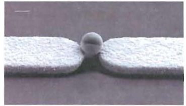
J. Phys.: Condens. Matter 20 (2008) 374116                                                                          N Prokopuk and K-A Son

Figure 3. I – V properties of a metal–molecule–metal junction
formed by crossed wires with oligo(phenylene ethynylene)s [156].
Reprinted with permission from [156]. Copyright 2004 American
Chemical Society.

                                                                           Figure 4. Schematic of a gold cluster top-contact junction.
molecular film can lead to physical deformation in the bridging
molecules. The molecular component responds to the force
of the top contact through a simple conformational change in           metal junction [69]. Small gold clusters of a few nanometers
the molecule’s geometry or a contraction of the molecule’s             in diameter can serve as electrical leads that cover relatively
bonds and angles. Physical changes in the geometry of the              few molecules in the organic film compared to lithographically
molecule readily affect the molecule’s electronic structure            patterned top contacts, figure 4. To complete the metal–
and conductance compared to a stress-free junction [24, 25].           molecule–metal cluster circuit, the tip of a scanning probe
In a crossed-wire junction, the load between the wires can             connects to the individual metal clusters. A mechanism for
be changed by increasing or decreasing the Lorentz force.              anchoring the metal beads to the SAM such as covalently
With increasing pressure the conductance of oligo(phenylene            attaching the particles to the organic film is employed to
vinylene)s increase by a factor of 100 beyond what is expected         limit lateral motion of the metal particles. For gold clusters,
for a simple change in the contact area [10]. Presumably,              monolayers composed of symmetrically terminated bisthiols
deformations of the SAM layer results in a compression                 provide a distal thiol group disposed away from the surface
or stretching of the molecular elements and a change in                that is available to bind the metal cluster [15, 69]. The
the HOMO and LUMO energies and the molecule’s barrier                  number of molecular elements that bridge the conducting
height. Additionally, the formation of alternative (through            substrate and the metal particle can be further reduced by
space) pathways cannot be ruled out in these compressed                diluting the bisthiols in a monolayer composed primarily
systems. A similar pressure dependence is observed for                 of monothiols which lack the secondary thiol needed to
c-AFM measurements on SAMs of alkanethiols at high                     attach to the metal bead [15]. The conductance of metal–
force conditions [67]. In metal–molecule–metal junctions               molecule–metal cluster junctions constructed with carotenes
with more static configurations such as the top contacts               dispersed in highly resistive docosanthiol films are integer
formed by the thermal deposition of a metal layer on a                 multiples of a parent conductance that is assigned to that
LB film, subtle pressure effects can still contribute to the           of a single carotene [15]. Resistance between the probe
variability in the configuration and tunneling properties of the       tip and the metal particle can lead to charging or Coulomb
organic component. Consequently, the measured resistance of            blockade events which manifest in the I – V properties of
molecular wires varies depending on the specific experimental          the junction and require deconvolution from the inherent
conditions used to connect the molecule to electrical leads.           properties of the molecular component. Larger gold particles
For example, scanning probe measurements (c-AFM and                    (>5 nm) can reduce both the tip bead resistance and Coulomb
STM) and Hg-drop experiments on monolayers of alkyl                    charging barriers [70]. Unlike the break junctions formed by
bis and monothiols result in molecular conductivities that vary        direct contact between the scanning probes and bisthiols in
by several orders of magnitude for alkyl chains of similar             a monolayer or the crossed-wire platform, the conductance
length [68].                                                           values of molecular junctions formed with metal beads are not
                                                                       as strongly dependent on the force exerted by the contacting
                                                                       probe used to connect the metal cluster to the external circuit.
2.4. Metal beads
                                                                            Integrated circuits constructed from metal bead top
Metal beads or colloidal metal particles dispersed on a SAM            contacts require that the clusters assemble in an organized
provided one of the early top contacts for metal–molecule–             and controlled fashion.       Monolayers of pure bisthiols

                                                                   6
J. Phys.: Condens. Matter 20 (2008) 374116 N Prokopuk and K-A Son
Figure 5. Micrograph of a magnetic bead bridging two Ni80 Fe20
electrodes. The scale bar is 1 μm [14]. Reused with permission
from [14]. Copyright 2005, American Institute of Physics. Figure 6. Photograph of a mercury top contact on a SAM-coated
silver surface [78]. Reprinted with permission from [78]. Copyright
2002 Elsevier.
serve as sticking boards to gold clusters without providing
any means to limit or manage the placement of the top
contacts. Bisthiols dispersed in monothiol layers limit the Subsequent work [77–81] with mercury top contacts
gold cluster deposition only to the sites where the bisthiols demonstrated that liquid leads can be employed with solid
are located [70]. However, selecting the placement of silver and gold bottom contacts with organic thiols and
the bisthiols within a film of monothiols poses it’s own disulfide monolayers, figure 6. In these devices the
challenges. Kushmerick demonstrated the directed assembly morphology of the solid metal electrode greatly influences
of metal colloid top contacts with magnetic particles made the conductance of the junction [81]. The interface of
by sequentially coating silica microspheres with nickel and highly crystalline silver films in a mercury-bilayer-silver
gold [14]. The ferromagnetic nickel layer contributes a device yields more reproducible I –V behavior with a narrower
magnetic moment which provides a mechanism for controlling current density distribution than interfaces formed with
the placement and orientation of the particle. The Au/Ni less crystalline silver. Unlike the mercury-bilayer-mercury
particles undergo directed assembly on arrays of magnetic junctions that contain SAMs of the same molecule on each
electrodes coated with SAMs, figure 5. In this geometry, metal surface, junctions with mercury and a solid metal contact
the metal beads span two electrodes coated with a SAM can be constructed with dissimilar SAMs on the two leads
and two metal–molecule–metal junctions are formed in series. allowing for asymmetric bimolecular circuits. Rectification in
Parsons used dielectrophoresis to trap nanoparticle–molecule– tunneling currents between mercury-bilayer-silver (and gold)
nanoparticle dimers between electrodes [71]. The gold was observed with bilayers composed of two different SAMs,
nanoparticle dimers exhibit stable I –V properties with bridged one containing a tetracyanoquinyl group and the second an n -
oligomeric phenylenes. Electrostatic trapping of single gold alkyl chain [79]. Bilayers composed of alkyl chains of two
nanoparticles between metal electrodes separated by tens different lengths also exhibit rectification [80]. Interestingly,
of nanometers [72] and coated with organic monolayers a single layer of alkyl thiolate between two mercury drops
also forms stable metal–molecule–colloid–molecule–metal produce symmetric I –V curves indicating no rectification
bijunctions [73, 74]. Directing large numbers of metal particles despite the two different metal–molecule interfaces (covalent
between patterned electrodes promises a straightforward, if Hg–S and noncovalent Hg... CH3 –) [82]. The resistance of
cumbersome, method for generating arrays of molecular the single-molecule junction is an order of magnitude greater
junctions. than that obtained for bilayers containing the same number of
carbon atoms indicating that the nonbonding methyl–mercury
2.5. Mercury drops junction is significantly more resistive than the methyl–methyl
While neither structurally robust nor easily integrated into interface of a Hg-bilayer-Hg device.
micro-or nano-sized circuits, liquid mercury contacts to While mercury top contacts are unlikely to find
molecular resistors and switching elements provide a simple applications in the construction of integrated circuits, a number
and low-cost method for studying metal–molecule–metal of metal–molecule–metal junctions generated with liquid
junctions. Mercury contacts to molecular circuits were first mercury top contacts have produced particularly significant
reported by Whitesides [75] with SAMs of organothiols results for molecular and solid-state electronics. In one set of
or disulfides separating two mercury drops. The initial experiments [83, 84], the conductance of electroactive bilayer
work focused on the alkyl layers as nanoscale dielectrics films of (NH3 )5 Ru(pyridyl) sandwiched between mercury
in capacitors [11, 75]. In these experiments, the liquid drops was observed to change by several orders of magnitude
mercury surfaces provide smooth and defect-free platforms upon oxidation of the Ru-centers with a three-electrode
for SAMs of organosulfur compounds coating the two Hg- configuration, figure 7. The oxidation potential of the Ru-
droplets. Electrical measurements across the SAM-coated centers within the junction is not significantly shifted from
mercury drops yield conductance values for the organic bilayer that of the molecule dispersed in solution suggesting that
separating the liquid metal including the resistivity of the changes in the Ru-centers’ electronic structures are responsible
noncontacting gap between the SAM layers [76]. for the conductance increase. Mercury top contacts have
7J. Phys.: Condens. Matter 20 (2008) 374116 N Prokopuk and K-A Son
the metal–metal separation is crucial for the vacant nanogaps
to reliably form metal–molecule–metal junctions with consis-
tent and predictable properties. This added challenge poses a
significant hurdle to the development of vacant nanogaps in
molecular electronics applications. However, within the last
few years several new and promising methods have been re-
ported for generating nanospaced electrodes with well-defined
separations that are on the order of a few nanometers. Al-
though some of these new techniques have not been specif-
ically used to fabricate covalent metal–molecule–metal junc-
tions, their metal–metal spacings are readily suited for study-
ing electron tunneling across molecular dimensions.
Generating vacant nanogaps between metal electrodes
Figure 7. Transistor-like behavior of a requires a mechanism for controlling metal–metal separations
Hg-(pyridyl)Ru(NH3 )...5 (NH3 )5 Ru(pyridyl)Hg junction [83].
with subnanometer precision. To control and manipulate the
Reproduced with permission from [83]. Copyright 2004, John Wiley metal–metal distances with the necessary accuracy requires
& Sons, Inc. novel fabrication methods as these feature sizes are beyond
the limits of conventional lithography. Two strategies are
commonly employed for introducing nanogaps between metal
also been used to investigate Schottky diodes at Hg-molecule- electrodes. In one method, a feed back loop monitors in situ an
semiconductor junctions [85]. Diodes formed from mercury electronic signal during the deposition or erosion of metal that
drops on silicon surfaces that are chemically modified with ultimately forms the electrical leads. The fabrication process
insulating n -decyl chains exhibit near-ideal rectifying behavior is immediately stopped once a predetermined resistance is
that is superior to similar devices fabricated with the native obtained. For example, electrochemically plating metal atoms
silicon dioxide layer as the insulator. The excellent diode on lithographically patterned leads reduces the separation
behavior and model energetics observed for the Hg-decyl- between the electrodes and the conductance of the junction
silicon junctions indicates that Hg atom migration and silicide rises when the electrodes approach the tunneling distance and
formation are not contributing to the dynamics of the charge the current rapidly increases. The feedback loop can be used
transfer process at these Schottky junctions. The simplicity of in conjunction with a variety of techniques for depositing or
forming liquid mercury top contacts provides a simple route removing metal in the junction fabrication. In the second
to metal–molecule–metal and metal–molecule-semiconductor method, a sacrificial layer is used to temporarily separate the
junctions with few electrical artifacts resulting from the two electrodes during the fabrication process. The spacer
introduction of the top contact. layer determines the electrode separations and is subsequently
removed leaving a vacancy between the metal electrodes. In
3. Vacant nanogaps order to obtain separations of 1–3 nm, the spacer itself must
be molecular or atomic in nature. Both thin atomic films and
Constructing vacant nanogaps with specific electrode geome- molecular layers have been used as the templating agent for
tries and separations that are suitable for molecular electronic generating vacant nanogaps and arrays of empty junctions. The
application is somewhat more challenging than the top-contact level of control over the electrode separations and geometries
approach. Unlike the top-contact method in which the metal varies with the specific method and materials used to form the
contacts are built around a specific molecular element that dou- nanogaps.
bles as a template for defining the metal–metal separation, fab- Despite the significant challenges of fabricating vacant
ricating vacant gaps with nanometer dimensions requires al- nanogaps, the benefit of being able to characterize the
ternative strategies to control the metal–metal distance (gap molecule-free junction and compare it to the completed metal–
sizes) with great precision. Small deviations in the electrode molecule–metal device provides substantial motivation for
separations can prevent the molecular component from span- pursuing the vacant nanogap strategy. By first characterizing
ning the two electrodes. For example, biphenyl-4,4 -dithiol the electronic properties of the pristine empty gap ‘as made’,
can effectively bridge gold electrodes that accommodate the the resistance or switching characteristics of the molecular
10.7 Å separating the sulfur atoms. A deviation of 1 Å in component can be investigated with the knowledge that any
the metal–metal separation can prevent the molecule from co- changes in the gap’s resistivity are due to the molecular
valently bridging the metal leads. Smaller gaps require the element. Vacant gaps with dubious electrical properties are
molecule to adopt a tilted orientation to fit within the available easily identified and discarded prior to the molecular studies.
space which may provide alternative tunneling pathways or de- Since the molecular component is inserted only after the
formations in the molecule and the molecular orbitals involved fabrication of the metal leads is complete, complications
in electronic coupling [25]. For molecular electronic applica- arising from the deposition of metal vapor on the organic films
tions, a large distribution in electrode spacings can compro- are not a concern with vacant nanogaps.
mise device yields as gaps that are too large or too small may A second advantage of constructing metal–molecule–
result in irregular electrical properties. Thus, spatial control of metal junctions from vacant nanogaps is the accessibility of
8J. Phys.: Condens. Matter 20 (2008) 374116 N Prokopuk and K-A Son
generate covalent gold–molecule–gold contacts. The molecu-
lar element is often a symmetric bisthiol with the two sulfur
groups disposed at opposite ends of the molecule. This geom-
etry allows the molecule to spontaneously bridge the metal–
metal gap. One disadvantage of inserting the molecular com-
ponent into a premade nanogap is that asymmetric molecules
will randomly orient within the junctions instead of aligning
their dipoles in parallel. More sophisticated methods are re-
quired to spontaneously align the molecule dipoles such as the
use of an electric field between the electrodes during the self-
assembly process. Also, exposing the entire circuit to an organ-
othiol solution will coat all exposed gold surfaces with the
thiol. To some extent, thiolate coverage can be electrochem-
ically deposited on specific electrodes [92]. Specific strate-
gies for generating the vacant nanogaps are discussed in more
Figure 8. Three-electrode devices formed with electromigration gaps
and Co-polypyridyl complexes. The topographic micrograph (top detail.
left) shows the nanogaps with a scale bar of 100 nm. The I – V curves
are acquired at gate voltages raging from −0.4 V (red) to −1.0 V 3.1. Mechanical break junctions
(black) at −0.15 V intervals [107]. Reproduced with permission
from [107]. Copyright 2002 Nature Publishing Group. One of the first experiments to directly probe the electronic
properties of a metal–molecule–metal junction employed a
mechanically-induced break in a gold wire as the nanogap [5].
horizontal electrode geometries. With coplanar electrodes, the In these mechanical break junctions, a metal wire is deposited
underlying substrate can serve as a third electrical contact to on a flexible isolation substrate which rest on a piezoelectric
the molecular component bridging two metal leads, figure 8. fulcrum. The piezoelectric rod pushes upward and bends the
In these architectures, the insulating layer on the substrate flexible substrate fracturing the wire, figure 9. The size of the
serves as a dielectric separating a gate electrode from the gap in the broken wire can be controlled with subpicometer
bridging molecule. The gate toggles the electronic properties resolution by varying the force of the piezoelectric rod [93].
of the bridging molecule by inducing a polarizing electric field. In the initial experiments, the break in a gold wire was
The three-electrode configuration is similar to a conventional introduce with the wire immersed in a solution of benzene-
field effect transistor with the molecular component serving 1,4-dithiol which bridged the nanogap forming covalent
as the channel [86]. Importantly, the connection of the third linkages to the electrodes [5]. The molecular resistance in
electrode to the molecular circuit provides rational control over these experiments exhibited stepwise jumps of approximately
the electrical properties of the molecular channel. Mirrored 9 M as the gap size was increased suggesting that this
charges in the electrode can serve as counter charges to the was the inherent resistance of a single benzene-1,4-dithiol.
oxidized or reduced states of the molecular component. As Subsequent research has employed mechanical break junctions
the electronic structure of the molecule changes, the orbitals to measure the relative conductance of a variety of molecular
that participate in electronic coupling are altered resulting in structures [94, 95]. Since the cross-sectional area of the break
concomitant changes in the molecule’s conductivity. Care junctions are not well characterized, the number of molecules
must be taken to insure that the gap between the nanospaced bridging these nanogaps can only be estimated in order to yield
electrodes is free of electrical defects. Surface states on normalized conductances for the connecting molecules. By
the insulating dielectric layer can contribute to the electrical expanding the gap and breaking contact with the molecular
response of the device. In a molecule-sized device, only bridges, stepwise changes in the junction’s conductance reflect
a single surface defect is needed to replicate the electronic the electrical properties of the molecular components similar
properties of a molecule dominating the conductance of a to the top-contact experiments with scanning probe break
gap. By carefully characterizing the electronic properties of junctions. The mechanical break junctions are poorly suited
the vacant junction prior to introducing the organic thiols, the for building extended arrays of molecular circuits due to
absence of surface states can be confirmed to ensure that the the inherent size of the piezoelectric mechanism. Riel has
molecular element is providing the electrical response. successfully demonstrated the mechanical break junctions as
Nanogaps between metal leads can be fabricated using platforms for unipolar switches composed of oligo(phenylene
a variety of techniques including electromigration [87], elec- ethynylene)s [93]. Unless the piezoelectric components are
trodeposition/dissolution [88], shadow masking [89], focused significantly reduced in size, the mechanical break junctions
ion beams [90], or selective chemical etches [91]. Once the are unlikely to find more significant applications towards
metal electrodes are formed with the desired nanometer sepa- constructing integrated circuits of molecular electronics.
rations, the molecular component is subsequently inserted be-
tween the two electrodes. Importantly, the introduction of the
3.2. Electromigration
organic element must not disrupt the electrode geometries or
significantly change their composition. Organic thiols are of- Electromigration has been viewed for much of the last 100
ten used to take advantage of the soft gold-sulfur affinity and years as a detriment to integrated circuits and a source of
9J. Phys.: Condens. Matter 20 (2008) 374116 N Prokopuk and K-A Son
Figure 9. SEM image of a mechanical break junction (left) and schematic showing the introduction of a nanogap by the bending of a
substrate (right) [93]. Reproduced with permission from [93]. Copyright 2006 Wiley-VCH Verlag GmbH & Co.
void, hillock, and whisker failures [96]. More recently the molecule-free nanogaps are attributed to the presence of mag-
phenomenon has been exploited to create nanometer-sized netic impurities in the gold islands and gold clusters between
gaps in conducting wires [87]. Electromigration results from the electrodes. The perceptible similarity in the electrical prop-
the transfer of momentum from an electrical current to the erties of the molecular components and metal clusters compli-
atoms and ions of the conductor. The momentum causes the cate the assignment of the Kondo effect’s origin.
metal atoms to move and, at high enough current densities, the The early work with conventional electromigration gaps
continuity of the wire is broken as gaps appear. The interest of produced relatively low yields of nanogaps (∼10–20%) that
electromigration to molecular electronics stems from the size provide measurable currents [6, 107, 110–112]. Moreover,
of the gaps which can be on the order of a few nanometers. each junction must be individually addressed during the
The importance of Joule heating in the migration of metal fabrication process. Modifications of the electromigration
atoms should not be ignored [97, 98] as the temperature of procedure have yielded simpler and more reliable routes
gold wires exposed to the current densities necessary for gap to fabricating arrays of nanogaps. Strachan and Johnson
creation can reach temperatures in excess of the melting point developed a strategy for fabricating vacant nanogaps in parallel
of the metal [99]. using a feedback-controlled electromigration method [103].
Electromigration-induced gaps can be inserted into gold The concurrent fabrication technique enables the generation
wires deposited on an insulating substrate by ramping of large arrays of nanospaced junctions. Similar fabrication
the current through the wire until the resistance suddenly
methods were demonstrated to produce clean and particle-
increases [87]. Feedback loops coupled with a nonlinear
free junctions [113]. Interestingly, the formation of
current ramp provide additional control over the electrical
electromigration gaps continues after the bias is removed
current and resistive heating [100, 101] which yields a smaller
and the gold atoms relax with significant movement in the
spread in the gap sizes and more control over the device
gold wire continuing [114]. Wires broken after the applied
dimensions [100, 102–104]. Scanning and transmission
voltage is stopped tend to result in cleaner gaps lacking the
electron microscopies have revealed the electromigration
process in situ with real-time video [105, 106]. metal clusters typical of the electromigration process. The
A significant concern with metal–molecule–metal junc- electrode separations can be controlled with field-emission
tions formed with electromigration gaps is the presence of currents that move gold atoms to further reduce the gap size
residual metal clusters or metal islands remaining between the after it has already been introduced [115]. With a combination
electrodes after the gap formation is complete. Electronic ar- of nonlinear current ramps, feedback loops, and field-emission
tifacts arising from the metal clusters can mask or mimic the currents, arrays of electromigration gaps can be fabricated that
electrical properties of the molecular component. Park’s early exhibit near-identical electrical properties.
studies with metal–molecule–metal junctions formed by elec- Perhaps, the most significant application of electromigra-
tromigration techniques demonstrated Coulomb blockade and tion nanogaps is the construction of three-electrode molecular
Kondo effects in chromium and vanadium complexes bridging devices [6, 107, 110–112]. Introducing vacant gaps in gold
the electrodes that are consistent with single-atom and single- wires deposited on a planar substrate allows the underlying
molecule devices [6, 107]. However, subsequent experiments material to serve as a third contact to the molecular compo-
on pristine nanogaps formed by electromigration revealed that nent. Single-molecule transistors have been fabricated from
the apparent vacant junctions also exhibit Coulomb blockade electromigration junctions with a variety of organic and in-
and Kondo effects despite the absence of the molecular ele- organic compounds serving as the channel material including
ment [104, 108, 109]. Electrical artifacts stemming from the redox active transition metal complexes and oligo(phenylene
10J. Phys.: Condens. Matter 20 (2008) 374116 N Prokopuk and K-A Son
Figure 11. TEM of nanojunctions fabricated by electron-beam
Figure 10. Back scattering from standard substrates (top) results in lithography with ultra-thin Si3 N4 membranes. Inset in (a) and (c)
exposure of large sections of the PMMA resist. Thin Si3 N4 substrates show the full device with leads to external connections [12].
limit the exposure of the PMMA resist [12]. Reprinted with Reprinted with permission from [12]. Copyright 2006 American
permission from [12]. Copyright 2006 American Institute of Physics. Institute of Physics.
separations. Deep UV-photolithography offers an inexpensive
ethynylene)s [6, 107, 110–112]. The redox properties of the approach for patterning metal electrodes but the available
transition metals and conjugated organics provide a rational resolution limits feature sizes down to 50 nm. Conventional
mechanism for tuning the electronic structure and, hence, the electron-beam lithography can push the limit to 10 nm.
conductance of the bridging molecule. In these experiments, While these dimensions are still too large for measuring
gold wires are chemically modified with the molecular element tunneling currents through single molecules, they are well
prior to introducing the gaps via electromigration. After the suited for investigating the electronic properties of polymers,
current is ramped and the gap forms, a relatively small yield nanocrystals, and liquids [116–119]. Photolithographically
of devices (10–20%) exhibit electrical properties that are con- patterned leads often serve as starting points for generating
sistent with a metal–molecule–metal junction. The underlying smaller molecular-sized gaps by depositing additional metal
gate electrode is used to toggle the conductance of the molec- on the electrodes. Nanometer-sized features are possible with
ular bridge between on/off states. For example, the resistivity advanced lithographic techniques which adapt conventional
of polypyridyl cobalt complexes change by several orders of photo- and electron-beam lithography for generating nanogaps
magnitude upon applying a gate voltage of 0.6 V [107]. How- with molecular dimensions.
ever, the exact mechanism responsible for the observed switch- Fischbein and Drndić developed a strategy for generating
ing is inconclusive [111], as the presence of gold clusters or subnanometer features using conventional electron-beam
particles in the electromigration gap has not been eliminated lithography coupled with a thin-film substrate [12]. The
vida supra [104, 108, 109]. Additionally, the effect of the high resolution of electron-beam lithography is primarily limited
temperature in the gold wire during the ramping of the elec- by electron back scattering from the substrate [120, 121],
tromigration current is likely to adversely affect the molecules figure 10. By utilizing a 100 nm thick silicon nitride membrane
adsorbed to the surface [97–99]. Any solid carbides that might as the substrate, the back scattering of the electron-beam
form from deleterious chemical reactions between the molecu- was considerably reduced allowing a significant improvement
lar components and the gold electrodes or underlying substrate in the resolution of the irradiated area. Metal leads with
can also contribute electrical artifacts to the current profiles of subnanometer spacings can be patterned and imaged directly
the junctions. with a TEM using the thin membranes, figure 11. However,
the thin substrates required for the transparent electron-beam
lithography are very fragile and the prospects of scaling
3.3. Lithography
the technology for mass production necessitate a significant
Integrated circuits containing hundreds of thousands or engineering effort.
millions of nanogaps require a reliable and low-cost method Oblique angle shadow evaporation of metal vapor offers
for generating the metal electrodes with the necessary an alternative approach to constructing large arrays of
11You can also read