Low-Temperature Synthesis of Vanadium Dioxide Thin Films by Sol-Gel Dip Coating Method
←
→
Page content transcription
If your browser does not render page correctly, please read the page content below
Hindawi
Journal of Nanotechnology
Volume 2021, Article ID 4868152, 7 pages
https://doi.org/10.1155/2021/4868152

Research Article
Low-Temperature Synthesis of Vanadium Dioxide Thin Films by
Sol-Gel Dip Coating Method

          Ladawan Chotirat ,1,2,3 Sutham Niyomwas,1,2,4 Witthawat Wongpisan,5
          and Sitthisuntorn Supothina 5
          1
            CENE Center of Excellence in Nanotechnology for Energy, Prince of Songkla University, Hat Yai 90112, Thailand
          2
            CEMME Center of Excellence in Metal and Materials Engineering, Prince of Songkla University, Hat Yai 90112, Thailand
          3
            Department of Mining and Materials Engineering, Faculty of Engineering, Prince of Songkla University, Hat Yai 90112, Thailand
          4
            Department of Mechanical Engineering, Faculty of Engineering, Prince of Songkla University, Hat Yai 90112, Thailand
          5
            National Metal and Materials Technology Center, Thailand Science Park, Pathum Thani 12120, Thailand

          Correspondence should be addressed to Sitthisuntorn Supothina; sitthis@mtec.or.th

          Received 5 April 2021; Accepted 4 June 2021; Published 17 June 2021

          Academic Editor: Hongmei Luo

          Copyright © 2021 Ladawan Chotirat et al. This is an open access article distributed under the Creative Commons Attribution
          License, which permits unrestricted use, distribution, and reproduction in any medium, provided the original work is
          properly cited.
          The vanadium dioxide (VO2) thin films were synthesized by sol-gel dipping on a glass slide substrate at low temperature of 500°C
          in a vacuum tube furnace at a pressure of 2 × 10⁻³ mbar by 2-step calcination without an intermediate gas purging. Synthesis
          conditions, including temperature, vacuum pressure, and calcination steps in the vacuum tube furnace, were investigated to find
          the optimum condition that promoted the formation of VO2 phase. It was found that the 2nd calcination step was very important
          in realizing the monoclinic vanadium dioxide (VO2 (M)). The results of the valence electron analysis revealed the outstanding
          phase of VO2 and a small amount of V2O5 and V2O3 phases. The small crystallites of the VO2 were homogeneously distributed on
          the surface, and the grain was of an irregular shape of ∼220−380 nm in size. The film’s thickness was in a range of 69−74 nm. The
          film exhibited a metal-to-insulator transformation temperature of ∼68oC and good thermochromic property. Visible optical
          transmittance remained at ∼40−50% when the sample’s temperature changed from 25 to 80°C for a near infrared (NIR) region.

1. Introduction                                                         transmittance, makes the vanadium dioxide a promising
                                                                        candidate as thermochromic coating for a variety of devices
Vanadium oxide presents a partly-filled 3d orbital, leading to           such as smart windows, tunable absorbers and emitters, and
the formation of several oxides such as VO, V2O3, V4O7,                 thermal rectification [4, 5].
VO2, V2O5, and V6O13, which all belong to the series of                     The thermochromic VO2 (M) thin films have been
Magneli (VnO2n-1) and Wadsley (V2nO5n-2) systems [1–3].                 prepared by several methods. The most typical methods
Among these oxides, monoclinic vanadium dioxide (VO2                    include physical vapor deposition, chemical vapor deposi-
(M)) has gained most attention owing to its fascinating                 tion, and sol-gel method. The physical and chemical vapor
thermochromic property that can switch a phase structure                depositions can precisely control the stoichiometry of films
reversibly between a monoclinic (semiconductor) and a                   by monitoring oxygen partial pressure. However, the
rutile (metal) phase at about 68°C [3, 4] in response to                complex deposition processes and expensive equipment
external stimuli, leading to dramatic changes in the electrical         significantly limit their practical applications [6, 7]. The sol-
and optical properties. The change of optical property from             gel method has been widely employed for material inves-
infrared-transmitting at low temperature to infrared-                   tigation because of several advantages. For instance, it can be
reflecting at temperatures higher than the monoclinic-rutile             coated on complex shape, large substrate. The process is of
phase transition temperature, while maintaining the visible             low cost, and there is easy control of reaction kinetics and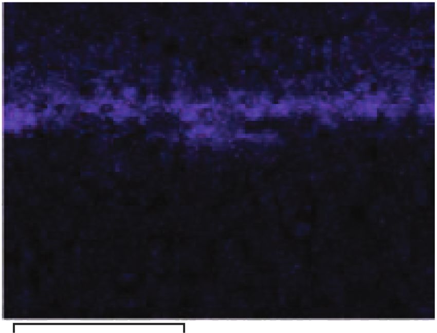
2                                                                                                     Journal of Nanotechnology

atomic doping. In addition, lower calcination temperature is        deposited thin films were dried in ambient air for 24 h. The
typically required to obtain crystalline structure [8–10]. In a     dried thin films were calcined at room temperature, 400, 450,
typical sol-gel process for VO2 preparation, a V5+-con-             and 500°C, in vacuum tube furnace at pressures of 2 × 10⁻²
taining precursor is firstly prepared, and then the precursor        and 2 × 10⁻³ mbar. To investigate an effect of heat treatment,
is deposited onto a clean, hydrophilic substrate through dip        calcination was conducted by 1- and 2-step calcination, in
or spin coating. The obtained sample is dried and calcined          which each step employed a heating rate of 2°C/min and
typically at ≥600°C [11–13] to transform an amorphous               soaking time of 3 h. For the 1-step calcination, the thin films
phase to a desired crystalline structure. Meanwhile, part of        were heated in a tube furnace to 400, 450, and 500°C, soaked
V5+ ions was reduced to V4+ ions [8, 11].                           at this temperature for 3 h, and cooled down to room
    For commercial applications, such as smart window               temperature. The 2-step calcination was carried out in a tube
coating, glass is the desirable substrate. The soda lime glass is   furnace at 500°C using the same heating and cooling cycles,
the most common and cheapest one [14, 15]. Considering              noted that the glass slide substrate employed in this work
that, for wet-chemical processes, the crystalline VO2 phase is      began to soften at a temperature of ∼500°C; thus, calcination
typically formed by a high-temperature treatment process.           temperature did not exceed 500°C. Process parameters for
This would restrict the calcination of VO2 thin films on the         film deposition are provided in Table 1.
soda lime glass substrate which is generally tempered at
approximately 600oC. The glass begins to soften at this             2.2. Thin Film Characterization. Crystal structure charac-
temperature. The strength of the tempered glass would be            terization of the thin films was performed by using an X-ray
weakened after VO2 thin film deposition at temperatures              diffractometer (XRD; Rigaku TTRAX III). Morphology and
higher than its softening temperature. Therefore, for soda          thickness were studied by using a scanning electron mi-
lime glass panel substrates, low-temperature deposition             croscope (SEM; Quanta 400 FEI) performed in a top and
(
Journal of Nanotechnology 3
Table 1: Fabrication parameters of VO2, V2O5, and V6O13 thin films.
Phase Furnace temperature (oC) Vacuum pressure (mbar) Calcination (step)
Amorphous Room temperature 2 × 10⁻² 1
V2O5 400 2 × 10⁻² 1
V2O5 450 2 × 10⁻² 1
VO2+V2O5 500 2 × 10⁻² 1
VO2+V2O5+V6O13 500 2 × 10⁻³ 1
VO2 500 2 × 10⁻³ 2
Relative intensity (a.u.)
Relative intensity (a.u.)
500°C
450°C
2 × 10⁻³ mbar
400°C
Room temp 2 × 10⁻² mbar
15 20 25 30 35 40 45 50 55 60 15 20 25 30 35 40 45 50 55 60
2 theta (degree) 2 theta (degree)
VO2 VO2
V2O5 V2O5
V6O13
(a) (b)
Relative intensity (a.u.)
2-step calcination
1-step calcination
15 20 25 30 35 40 45 50 55 60
2 theta (degree)
VO2
V2O5
V6O13
(c)
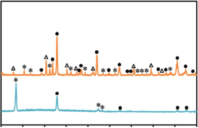
Figure 1: XRD patterns of the vanadium oxide thin films prepared at various conditions: (a) T � RT, 400, 450, and 500°C (P � 2 × 10⁻² mbar, 1-step
calcination), (b) P � 2 × 10⁻² and 2 × 10⁻³ mbar (T � 500°C, 1-step calcination), and (c) 1- and 2-step calcination (P � 2 × 10⁻³ mbar, T � 500°C).
patterns of the vanadium oxide thin films after calcined at amorphous nature signified by the absence of diffraction
various conditions summarized in Table 1. peak. XRD patterns of the thin films calcined at 400 and
For the 1-step calcination (Figure 1(a)), the temperatures 450oC show diffraction peaks at 18.7o, 20.1o, 24.7o, 26.2o,
were controlled at 400, 450, and 500oC, respectively, and the 30.1o, 31.3o, 32.4o, 34.8o, 37.6o, 38.6o, 48.6o, and 51.1o, which
pressure was fixed at 2 × 10⁻² mbar. XRD analysis of the correspond to the (001), (101), (201), (110), (301), (400),
dried thin film (denoted as “room temperature”) revealed (111), (211), (401), (311), (302), and (012) planes,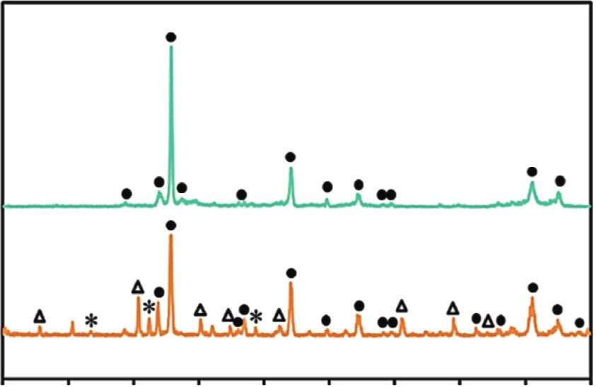
4 Journal of Nanotechnology
respectively, of the orthorhombic V2O5 (ICCD card no. 04- 2.6, and 0.6 At.%, respectively. The V and O correspond to
015-2250). Increasing the calcination temperature results in the VO2 thin film, and the others (and part of O) correspond
an increased intensity of the XRD peaks, indicating an in- to the glass slide substrate. The elemental mappings of Si
crease of film’s crystallinity. For the thin film calcined at from the glass substrate and V from the VO2 film
500oC, its XRD pattern reveals the peaks at 27.7o, 42.5o, (Figures 2(e) and 2(f )) reveal homogeneous distribution of
55.7o, and 57.8o corresponding to the (011), (210), (220), and the VO2 grains in the thin film.
(211) planes, respectively, of the monoclinic VO2 (ICCD Typical surface XPS spectra of the VO2 sample are
card no. 00-043-1051). Diffraction peaks of the V2O5 at depicted in Figure 3. Detail-scan spectra were employed to
18.7o, 37.6o, and 38.6o, which correspond to the (001), (401), investigate the valence electron of the V and O and to
and (311), planes, respectively, of the orthorhombic V2O5 confirm phase purity of the thin films. According to the
(ICCD card no. 04-015-2250) are also observed. This result standard binding energy, a typical two-peak structure (2p3/2
indicates a coexistence of the V2O5 and VO2 phases by the 1- and 2p1/2) due to the spin-orbit splitting was observed [19].
step calcination at 500oC. To further investigate the effect of The peaks at 516.1 and 523.8 eV shown in Figure 3(a)
4+ 4+
calcination condition, the pressure of the vacuum tube correspond to binding energies for V2p3/2 and V2p1/2 , re-
furnace was varied to 2 × 10⁻³ mbar, while the temperature spectively. The peaks at 517.6 eV and 525.2 eV correspond to
was maintained at 500oC. As shown in Figure 1(b), XRD 5+
V2p3/2 5+
and V2p1/2 , respectively. This result indicated atmo-
patterns of the orthorhombic V2O5 are dramatically reduced spheric oxidation of a small amount of V5+ at the surface of
while those of the monoclinic VO2 are enhanced. In addi- the sample. The binding energy of O1s appears at 530.0,
tion, diffraction peaks at 17.9o, 25.7o, 30.3o, 32.6o, 36.3o, 531.8, and 532.8 eV, which correspond to the V-O bonding,
45.8o, 50.1o, and 52.3o corresponding to the (002), (110), O–-H bonding, and part of physically adsorbed H2O, re-
(400), (−402), (−113), (005), (020), and (220) planes, re- spectively, as shown in Figure 3(b). Besides these major
spectively, of the V6O13 phase (ICCD card no. 04-008-4854) energy levels, a number of less intense satellite peaks are also
are present. This result indicates that lower vacuum pressure, present. These V2p satellite peaks are attributed to the V2O3.
the less amount of oxygen, promoted the formation of the The XPS composition analysis result confirms the presence
VO2, as well as the V6O13 minor phase. This reduction of VO2, as well as a small amount of V2O5 and V2O3 [25, 26].
condition at a temperature above 400oC and a pressure
below 2 Pa (2 × 10⁻² mbar) which caused the conversion of
3.2. Electrical Properties of VO2 (M) Thin Films.
V2O5 thin films to VO2 has been reported by Ningyi et al.
Figure 4(a) illustrates the temperature dependence of
[22]. It was observed that the reduction process followed the
electrical resistance of the VO2 thin films on the soda lime
sequence as V2O5⟶V3O7⟶V4O9⟶V6O13⟶VO2,
glass prepared by the 2-step calcination process at 500oC
namely, from VnO2n+1 (n � 2–4, 6) to VO2. Therefore, lower
with the pressure of 2 × 10⁻³ mbar. The hysteresis loop
pressure favoured VO2 formation caused by the oxygen
indicates the metal-to-insulator transformation and the
deficiency [22, 23]. To further investigate the effect of cal-
quality of the thin film. It was observed that surface re-
cination time, the calcination soaking time was increased
sistance of the thin film decreased upon the heating
from 3 to 24 h. It was found that the thin film consisted of
process and increased upon the cooling process. The
only V2O3 phase.
transition temperature, determined according to equation
Figure 1(c) shows XRD patterns of the thin films pre-
(1), was approximately 68oC (Tc � (80oC + 56oC)/2).
pared by means of 1-step and 2-step calcination in the
Furthermore, resistivity profile of the VO2 thin films was
vacuum tube furnace at 500oC with the pressure of
nearly flat above the room temperature (semiconductor
2 × 10⁻³ mbar. It is evident that only diffraction peaks of the
phase), indicating that the transition occurs at 68oC
monoclinic VO2 are present in the film prepared by 2-step
(metal-insulator transition phase) and constant at 80oC
calcination caused by the reduction process of V2O5 and
(metal phase), respectively [7, 27]. The VO2 thin films
V6O13.
were transformed from monoclinic to tetragonal (rutile)
SEM surface analysis of the VO2 thin film prepared by
phase at the transition temperature.
the 2-step calcination process at 500oC with the pressure of
2 × 10⁻³ mbar (Figures 2(a) and 2(b)) reveals very fine VO2
grains with irregular shape of ∼220–380 nm in size sur- 3.3. Optical Properties of VO2 (M) Thin Films. Figure 4(b)
rounded by an amorphous phase of anhydrous vanadium illustrates the optical transmittance spectra measured at
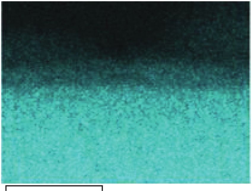
oxide from gelation [24]. Film’s thickness determined from a 25 and 80oC of the VO2 thin films. Visible optical
cross-sectional image (Figure 2(c)) is approximately transmittance remains at ∼40–50% when the sample’s
69–74 nm. Elemental composition analyzed by EDS temperature changes from 25 to 80oC. However, for a near
(Figure 2(d)) reveals that the sample comprises of Si, O, Na, infrared (NIR) region wavelength range of 800–2500 nm,
Ca, V, Mg, and Al at the amount of 30.1, 51.0, 8.5, 5.7, 1.5, the optical transmittance measured at 25oC is clearly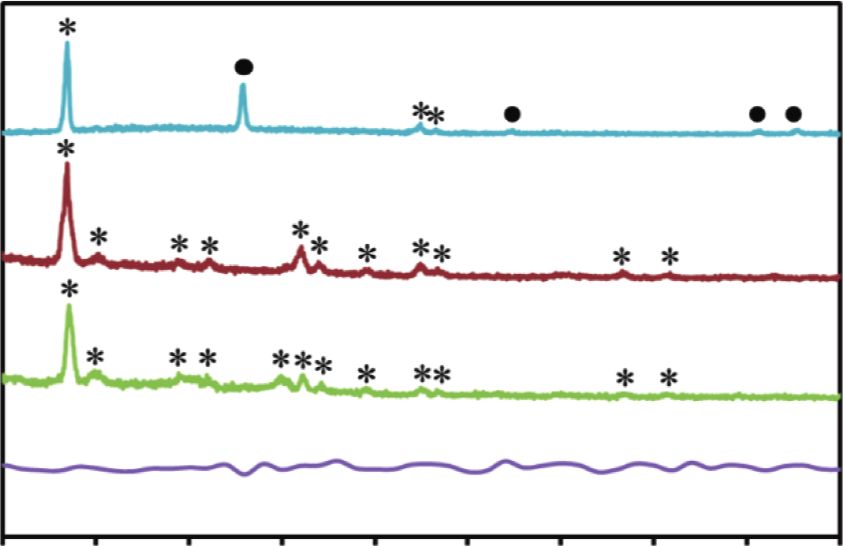
Journal of Nanotechnology                                                                                                               5

                                                         1μm                                                      1 μm

                                    (a)                                                           (b)

                                                                            O        Si
                                                                            V

                    74nm    71 nm              69 nm     71 nm   71nm

                                                                                Na

                                                                                 Mg
                                                                                  Al            Ca
                                                                           Ca                            V
                                                       500 nm

                                    (c)                                                           (d)

                                                                                                             V

                                          Si

                 500nm                                                          500 nm
                                    (e)                                                           (f )

Figure 2: SEM images of the surfaceVO2 thin films at a resolution of x10,000 (a) and x50,000 (b) and cross-sectional image at x100,000 (c).
Film’s elemental composition analyzed by EDS (d), Si mapping (e), and V mapping (f ).

higher than that measured at 80oC. Moreover, the optical                indicating phase transition when the temperature is raised
transmittance increases with increasing wavelength at                   from 25 to 80oC. Thus, the thin film exhibits thermo-
25oC, while it reduces with increasing wavelength at 80oC,              chromic properties [28–30].
6 Journal of Nanotechnology
V(4+)2P3/2 V-O
V(5+)2P3/2
Intensity (cps)
Intensity (cps)
V(4+)2P1/2
V(5+)2P1/2 H2O O-H
V(3+)2P1/2
V(3+)2P3/2
528 526 524 522 520 518 516 514 512 535 533 531 529 527
Binding energy (eV) Binding energy (eV)
(a) (b)
Figure 3: XPS spectra of the VO2 thin film; curve-fitted V2p (a) and O1s (b) core level spectra.
100
1000000 90
80
Resistivity (Ω-cm)
Transmittance (%)
70
Hea
60
Tc ~ 68°C
ting
50
100000
Co
olin
40
g
30
20
10
10000 0
30 40 50 60 70 80 90 100 110 500 1000 1500 2000 2500
Temperature (°C) Wavelength (nm)
25°C
80°C
(a) (b)
Figure 4: Thermal hysteresis loop (a) and the optical transmittance spectra (b) of VO2 thin films.
4. Conclusions a conventional soda lime glass panel. In addition, as no
intermediate gas was employed during calcination, the
A simple and effective synthesis method for the preparation process would be suitable for large-scale fabrication.
of the vanadium dioxide thin films on the glass slide sub-
strate has been demonstrated by a sol-gel dip coating at low
temperature of 500oC in a vacuum tube furnace at a pressure Data Availability
of 2 × 10⁻³ mbar. The calcination was performed by 2 steps,
The data used to support the finding of this study are in-
in which thin films were heated in a tube furnace to 500oC at
cluded within the article.
a heating rate of 2oC/min, soaked for 3 h, and cooled down
to room temperature, and the same process was repeated.
The analyses revealed that the thin films consisted of Conflicts of Interest
monoclinic VO2 phase and a small amount of V2O5 and The authors declare that there are no conflicts of interest
V2O3 phases. The very fine VO2 grains with irregular shape regarding the publication of this paper.
of ∼220−380 nm in size were homogeneously distributed on
the surface. The film’s thickness was in a range of 69−74 nm. Acknowledgments
The monoclinic to tetragonal (rutile) phase transition
temperature was 68oC. The thin films exhibited good This study was financially supported by the Thailand
thermochromic properties. The low-temperature synthesis Graduate Institute of Science and Technology (TGIST, no.
would be beneficial for thermochromic thin film coating on SCA-CO-2559-2296-TH) in National Science and
Journal of Nanotechnology                                                                                                                      7

Technology Development Agency (NSTDA), Center of                               plasma-treated glass slides by aqueous sol-gel method,” Ap-
Excellence in Nanotechnology for Energy (CENE), Center of                      plied Surface Science, vol. 357, pp. 2069–2076, 2015.
Excellence in Metal and Materials Engineering (CEMME),                  [15]   L. Chotirat, S. Niyomwas, S. Supothina, W. Wongpisan, and
Graduate School of Engineering, Prince of Songkla Uni-                         K. Waree, “Synthesis and electrical resistance property of
                                                                               vanadium oxide thin films by DC magnetron sputtering,”
versity. The authors extend their thanks to the Department
                                                                               Materials Science Forum, vol. 998, pp. 185–190, 2020.
of Mining and Materials Engineering, Faculty of Engi-                   [16]   P. Phoempoon and L. Sikong, “Phase transformation of VO2
neering, Prince of Songkla University.                                         nanoparticles assisted by microwave heating,” The Scientific
                                                                               World Journal, vol. 2014, Article ID 841418, 8 pages, 2014.
                                                                        [17]   S. E. Zaki, M. A. Basyooni, M. Shaban et al., “Role of oxygen
References                                                                     vacancies in vanadium oxide and oxygen functional groups in
                                                                               graphene oxide for room temperature CO2 gas sensors,”
 [1] M. M. Seyfouri and R. Binions, “Sol-gel approaches to                     Sensors and Actuators A: Physical, vol. 294, pp. 17–24, 2019.
     thermochromic vanadium dioxide coating for smart glazing           [18]   T. Ivanova, A. Harizanova, M. Surtchev, and Z. Nenova,
     application,” Solar Energy Materials and Solar Cells, vol. 159,           “Investigation of sol-gel derived thin films of titanium dioxide
     pp. 52–65, 2017.                                                          doped with vanadium oxide,” Solar Energy Materials and
 [2] P. Ashok, Y. S. Chauhan, and A. Verma, “Vanadium dioxide                  Solar Cells, vol. 76, no. 4, pp. 591–598, 2003.
     thin films synthesized using low thermal budget atmospheric         [19]   Z. Liang, L. Zhao, W. Meng et al., “Tungsten-doped vanadium
     oxidation,” Thin Solid Films, vol. 706, Article ID 138003, 2020.          dioxide thin films as smart windows with self-cleaning and
 [3] S.-E. Chen, H.-H. Lu, S. Brahma, and J.-L. Huang, “Effects of              energy-saving functions,” Journal of Alloys and Compounds,
     annealing on thermochromic properties of W-doped vana-                    vol. 694, pp. 124–131, 2017.
     dium dioxide thin films deposited by electron beam evapo-           [20]   P. Deepak Raj, S. Gupta, and M. Sridharan, “Nanostructured
     ration,” Thin Solid Films, vol. 644, pp. 52–56, 2017.                     V2O5 thin films deposited at low sputtering power,” Materials
 [4] W. Li, S. Ji, K. Qian, and P. Jin, “Preparation and charac-               Science in Semiconductor Processing, vol. 39, pp. 426–432, 2015.
     terization of VO2(M)-SnO2 thermochromic films for appli-            [21]   Y. Li, P. Jiang, W. Xiang, F. Ran, and W. Cao, “A novel
     cation as energy-saving smart coatings,” Journal of Colloid               inorganic precipitation-peptization method for VO 2 sol and
     and Interface Science, vol. 456, pp. 166–173, 2015.                       VO 2 nanoparticles preparation: synthesis, characterization
 [5] S. Taylor, L. Long, and L. Wang, “Fabrication and charac-                 and mechanism,” Journal of Colloid and Interface Science,
     terization of furnace oxidized vanadium dioxide thin films,”               vol. 462, pp. 42–47, 2016.
     Thin Solid Films, vol. 682, pp. 29–36, 2019.                       [22]   Y. Ningyi, L. Jinhua, and L. Chenglu, “Valence reduction
 [6] M. Kong, K. Egbo, Ch. P. Liu et al., “Rapid thermal annealing             process from sol-gel V2O5 to VO2 thin films,” Applied Surface
     assisted facile solution method for tungsten-doped vanadium               Science, vol. 191, no. 1–4, pp. 176–180, 2002.
     dioxide thin films on glass substrate,” Journal of Alloys and       [23]   K. Shibuya and A. Sawa, “Optimization of conditions for
     Compounds, vol. 833, Article ID 155053, 2020.                             growth of vanadium dioxide thin films on silicon by pulsed-
 [7] D. Li, Y. Shan, F. Huang, and S. Ding, “Sol-gel preparation and           laser deposition,” AIP Advances, vol. 5, Article ID 107118,
     characterization of SiO2 coated VO2 films with enhanced                    2015.
     transmittance and high thermochromic performance,” Ap-             [24]   Y. Liu, J. Liu, Y. Li et al., “Effect of annealing temperature on
     plied Surface Science, vol. 317, pp. 160–166, 2014.                       the structure and properties of vanadium oxide films,” Optical
 [8] J. Wu, W. Huang, Q. Shi et al., “Effect of annealing tem-                  Materials Express, vol. 6, no. 5, Article ID 259637, 2016.
     perature on thermochromic properties of vanadium dioxide           [25]   K. Li, M. Li, C. Xu et al., “VO2(M) nanoparticles with con-
     thin films deposited by organic sol-gel method,” Applied                   trollable phase transition and high nanothermochromic
     Surface Science, vol. 268, pp. 556–560, 2013.
                                                                               performance,” Journal of Alloys and Compounds, vol. 816,
 [9] Q. Song, H. Pang, W. Gong et al., “Enhancing phase-tran-                  Article ID 152655, 2020.
     sition sensitivity of tungsten-doped vanadium dioxide by
                                                                        [26]   D. Mukherjee, A. Dey, A. C. M. Esther et al., “Reversible,
     high-temperature annealing,” Materials Letters, vol. 161,
                                                                               repeatable and low phase transition behaviour of spin coated
     pp. 244–247, 2015.
                                                                               nanostructured vanadium oxide thin films with superior
[10] A. Pergament, G. Stefanovich, O. Berezina, and D. Kirienko,
                                                                               mechanical properties,” Ceramics International, vol. 44, no. 8,
     “Electrical conductivity of tungsten doped vanadium dioxide
                                                                               pp. 8913–8921, 2018.
     obtained by the sol-gel technique,” Thin Solid Films, vol. 531,
                                                                        [27]   Z. Huang, S. Chen, B. Wang et al., “Vanadium dioxide thin
     pp. 572–576, 2013.
                                                                               film with low phase transition temperature deposited on
[11] O. Berezina, D. Kirienko, A. Pergament, G. Stefanovich,
                                                                               borosilicate glass substrate,” Thin Solid Films, vol. 519, no. 13,
     A. Velichko, and V. Zlomanov, “Vanadium oxide thin films
                                                                               pp. 4246–4248, 2011.
     and fibers obtained by acetylacetonate sol-gel method,” Thin
                                                                        [28]   R. Li, S. Ji, Y. Li, Y. Gao, H. Luo, and P. Jin, “Synthesis and
     Solid Films, vol. 574, pp. 15–19, 2015.
                                                                               characterization of plate-like VO2(M)@SiO2 nanoparticles
[12] N. Wang, S. Magdassi, D. Mandler, and Y. Long, “Simple sol-
                                                                               and their application to smart window,” Materials Letters,
     gel process and one-step annealing of vanadium dioxide thin
                                                                               vol. 110, pp. 241–244, 2013.
     films: synthesis and thermochromic properties,” Thin Solid
                                                                        [29]   C. Liu, S. Wang, Y. Zhou et al., “Index-tunable anti-reflection
     Films, vol. 534, pp. 594–598, 2013.
                                                                               coatings: maximizing solar modulation ability for vanadium
[13] A. Velichko, A. Pergament, V. Putrolaynen, O. Berezina, and
                                                                               dioxide-based smart thermochromic glazing,” Journal of
     G. Stefanovich, “Effect of memory electrical switching in                  Alloys and Compounds, vol. 731, pp. 1197–1207, 2018.
     metal/vanadium oxide/silicon structures with VO2 films
                                                                        [30]   Z. Qu, L. Yao, Y. Zhang, B. Jin, J. He, and J. Mi, “Surface and
     obtained by the sol-gel method,” Materials Science in Semi-               interface engineering for VO2 coatings with excellent optical
     conductor Processing, vol. 29, pp. 315–320, 2015.
                                                                               performance: from theory to practice,” Materials Research
[14] S.-D. Lan, C.-C. Cheng, C.-H. Huang, and J.-K. Chen,                      Bulletin, vol. 109, pp. 195–212, 2019.
     “Synthesis of sub-10 nm VO2 nanoparticles films with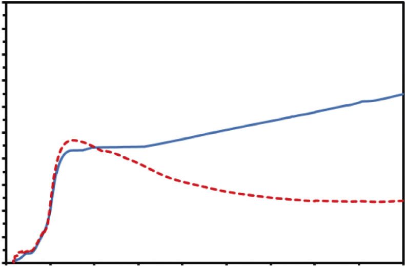
You can also read