Millimeter Wave Digital Arrays (MIDAS) - Proposers Day Dr. Timothy M. Hancock, MTO Program Manager - Defense Advanced Research ...
←
→
Page content transcription
If your browser does not render page correctly, please read the page content below
Millimeter Wave Digital Arrays (MIDAS)
                             Proposers Day

     Dr. Timothy M. Hancock, MTO Program Manager

                            January 26, 2018

           DISTRIBUTION A. Approved for public release: distribution unlimited.   1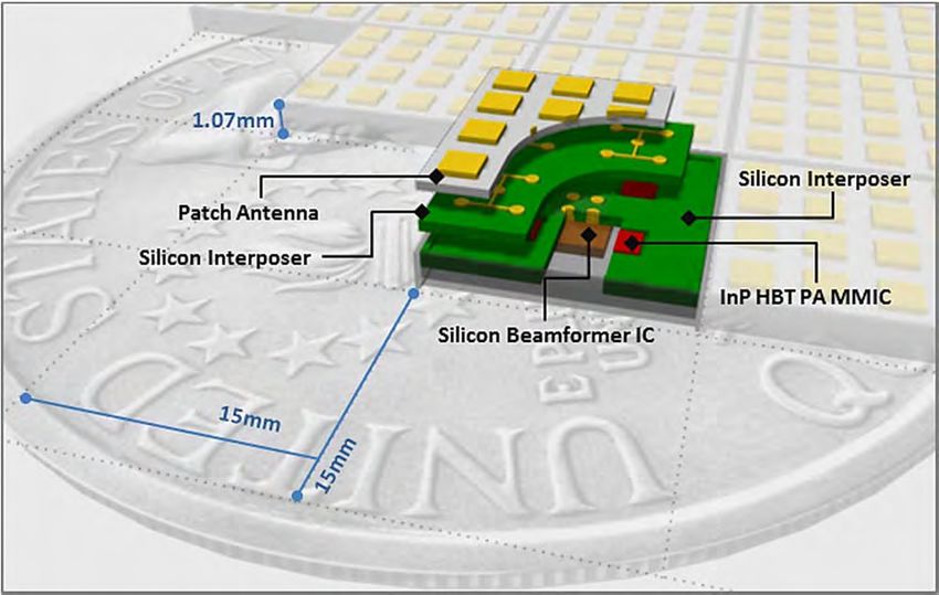
Agenda

•   0800-0900: Check-In
•   0900-0905: Welcome & Security
•   0905-0925: Contracting with DARPA
•   0925-1000: MIDAS Overview & Program Structure
•   1000-1015: Break
•   1015-1100: Q&A / Discussion
•   1100-1300: Poster & Networking Session

                          DISTRIBUTION A. Approved for public release: distribution unlimited.   2
Program Overview

DISTRIBUTION A. Approved for public release: distribution unlimited.   3
Evolution of Phased Arrays
                            1960’s              1970’s              1980’s             1990’s              2000’s                           2010’s       2020’s        2030’s
                λ/2
            Element                 Passive                                                Active Analog                                                     Digital
            Spacing
                                  Beamforming                                              Beamforming                                 THz                Beamforming
                                                                                                                                             MFRF
  W-band    1.5 mm                                                                                                                   NEXT

                                                                                                                                                     MIDAS        Leverage
  V-band    2.5 mm                                                                                          SMART                                                 device, circuit
                                                                                                                                                     mmW          & packaging
                                                                                      MAFET                                            ELASTx        Digital      investments
                                                                                                               AEHF
 Ka-band      4 mm
                                                                                                                (Pout = 5   W/cm2)

                                                                                                                                                     Arrays       to enable new
                                                                                HDMP                                                   DAHI                       architectures
                                                                         MIMIC                       WBGS-RF HEALICs
Ku/K-Band     8 mm
                                                             B-1B            JSTARS                TEAM COSMOS

  X-band    15 mm                                                                                                                                         ASIC development
                                                                                                                                        ACT               with commercial IP
                                                                                                 F-22         F-35
  C-band    20 mm                                                                Patriot
                                                                                 AN/MPQ-65

  S-band    40 mm                                                                                                                                       Enabled by
                                                                          AN/SPY-1                                                                      COTS & GaN
                          HAPDAR
   L-band   80 mm                                               Cobra                                                                   Space Fence
                                                                Dane

     UHF    400 mm                                                  PAVE
                                                                    PAWS

                                AN/FPS-85
             Adapted from: J. S. Herd and M. D. Conway, "The Evolution to Modern Phased Array Architectures," in Proceedings of the IEEE, vol. 104, no. 3, pp. 519-529, March 2016.

                                                   DISTRIBUTION A. Approved for public release: distribution unlimited.                                                        4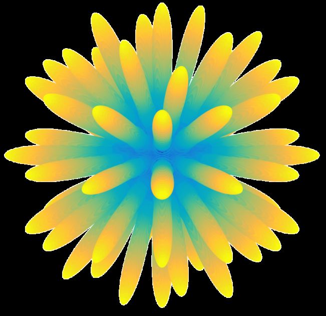
Millimeter Wave Systems

Physical Security Through Narrow Beams                                               Increased Throughput & Reliability
                                                                   Legacy     LegacySingle-Beam         Multi-Beam Multi-Beam
                                                                                               Single-Beam
                                                                Line Topology      Mesh Topology
                                                                           Line Topology               Mesh Topology
                                                                                              Mesh Topology      Mesh Topology

                             F-22
                       Intra-Flight Data                                                            10x          10-100x10x
                                                                                                               10x                  10x
                          Link (IFDL)
                                                            • Single beam         • Single beam
                                                                        • Single beam                     • Multiple beams
                                                                                              • Single beam             • Multiple beams
                                                            • One or two• link    • Multiple
                                                                          One or two  link link           • Multiple link
                                                                                              • Multiple link           • Multiple link
                                                                              Decreased
                                                              choices per choices
                                                                           node     choices
                                                                                  per         Discovery
                                                                                       node per node per
                                                                                                choices         Time
                                                                                                            choices
                                                                                                              node   per choices
                                                                                                                          node per node

                                                                              1000

                                                                  Neighbor Discovery Time
                                                                                                      Single-Beam
                                                                                   100                Multi-Beam

                                                                           (sec)
                                                                                       10
           F-35
                                                                                                                                  1000x
      Multi-function                                                                        1
     Advanced Data
                                                                                     0.1
      Link (MADL)
                                                                                0.01
                                                                                                0      50       100       150        200      250
                                                                                                      Number of Directional Sectors to Scan

    Millimeter wave links provide physical security, but pose networking challenges

                          DISTRIBUTION A. Approved for public release: distribution unlimited.                                                      5
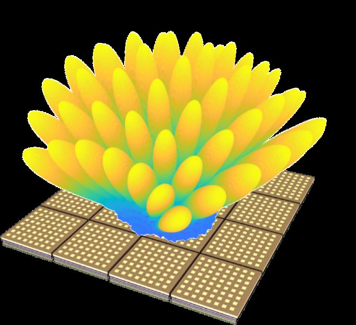
Multi-Beam Digital Arrays at Millimeter Wave

  Provide 4p Steradian Coverage for                                                The Common Digital Array Tile
 Multi-Beam Networked Communication                                                     at Millimeter Wave

                                                                                                        2 Core Tech Areas
                                                                                                      • Digital RF silicon tile
                                                                                                        at 18-50 GHz
                                                                                                      • Wideband antenna &
                                                                                                        T/R components

• High-gain in all directions for improved                                    Scalable Solution for Multiple Applications
  network performance                                                       • Line-of-sight tactical communications
• Wide bandwidth & frequency agility to                                     • Low-profile SATCOM
  adapt to future needs                                                     • Emerging LEO SATCOM

       Dominate the millimeter wave spectrum with wideband digital beamforming

                               DISTRIBUTION A. Approved for public release: distribution unlimited.                               6
Millimeter Wave Phased Arrays

            Analog Beamforming                                                                               Digital Beamforming
• Lowest power implementation                                                           • Challenging implementation requires R&D at mmW
• Single mixer/ADC after beamforming                                                    • Mixer/ADC at every element with beamforming DSP
• Challenging mmW design to manage phase & loss –                                       • mmW design kept to antenna front-end, minimal mmW
  leads to narrowband resonant designs                                                    routing/loss & line amps/distortion
• True-time-delay challenging & physically large
                              Passive (Lossy)                                           • Digital true-time-delay & multi-beam support

                     Φ

                                                                                                                                   Beamforming
                                                                                                                             ADC
                                Combiner

                    Φ                                                                                                    ADC

                                                                                                                                      DSP
                   Φ                                                                                                    ADC

                   Φ                                                                                                   ADC
                              Passive (Lossy)

                     Φ

                                                                                                                                   Beamforming
                                                                                                                             ADC
                                Combiner

                    Φ                                                                                                    ADC

                                                                                                                                      DSP
                   Φ                                                                                                    ADC

                                                                                                                                                 Beamforming DSP
                   Φ
                                                       Passive (Lossy)

                                                                                                                       ADC
                                                         Combiner
                              Passive (Lossy)

                     Φ

                                                                                                                                   Beamforming
                                                                                                                             ADC
                                Combiner

                    Φ                                                                                                    ADC

                                                                                                                                      DSP
                   Φ                                                                                                    ADC

                   Φ                                                                                                   ADC
                              Passive (Lossy)

                     Φ

                                                                                                                                   Beamforming
                                                                                                                             ADC
                                Combiner

                    Φ                                                                                                    ADC

                                                                                                                                      DSP
                   Φ                                                                                                    ADC

                   Φ                                                                                                   ADC

                                                DISTRIBUTION A. Approved for public release: distribution unlimited.                                               7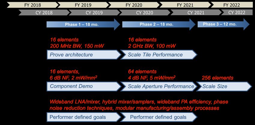
Multi-Beam Beamforming
Analog Beamforming Digital Beamforming
• Multiple copies of analog beamformer • No change in RF front-end with number of beams
• Power directly increases with number of beams • Size/power impact of additional DSP is small and scales
• Size directly increases with number of beams with technology
• Not scalable • Size/power scalable if front-end can be implemented
Passive (Lossy)
Φ
Combiner
Passive (Lossy)
Beamforming
ADC
Φ Φ
Combiner
Passive (Lossy)
ADC
Φ Φ Φ
DSP
Combiner
Passive (Lossy)
ADC
Φ Φ Φ Φ
Combiner
ADC
Φ Φ Φ
Φ Φ
Passive (Lossy)
Φ Φ
Combiner
Passive (Lossy)
Beamforming
ADC
Φ Φ
Combiner
Passive (Lossy)
ADC
Φ Φ Φ
DSP
Combiner
Passive (Lossy)
ADC
Φ Φ Φ Φ
Passive (Lossy)
Beamforming DSP
Combiner
Combiner
ADC
Φ Φ Φ
Passive (Lossy)
Combiner
Φ Φ
Passive (Lossy)
Passive (Lossy)
Φ Φ
Combiner
Passive (Lossy)
Combiner
Passive (Lossy)
Beamforming
ADC
Φ Φ
Combiner
Combiner
Passive (Lossy)
ADC
Φ Φ Φ
DSP
Combiner
Passive (Lossy)
ADC
Φ Φ Φ Φ
Combiner
ADC
Φ Φ Φ
Φ Φ
Passive (Lossy)
Φ Φ
Combiner
Passive (Lossy)
Beamforming
ADC
Φ Φ
Combiner
Passive (Lossy)
ADC
Φ Φ Φ
DSP
Combiner
Passive (Lossy)
ADC
Φ Φ Φ Φ
Combiner
ADC
Φ Φ Φ
Φ Φ
Φ
DISTRIBUTION A. Approved for public release: distribution unlimited. 8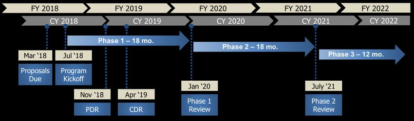
Program Overview

Program Objectives
• Explore the extent to which multi-beam systems can be employed at millimeter wave
  over extremely wide ranges of frequencies
• Digitization within the array itself enabled by ultra compact RF & mixed-signal design
  at millimeter wave
• A reduction in size and power of digital transceivers at millimeter wave that meet the
  high linearity requirements
• Develop and demonstrate a tile building block sub-array (>16 elements) that supports
  scaling to large arrays in the 18-50 GHz band and does not eliminate spatial degrees of
  freedom within the sub-array

Expected Areas of Research
• Innovative sampling and frequency conversion schemes with high linearity for receive and
  transmit
• Distributed LO/clock generation and synchronization for each element
• Wideband/efficient transmit/receive amplifiers & radiating apertures
• Novel manufacturing to realize the integration and packaging all of these components into
  a scalable tile building block

                          DISTRIBUTION A. Approved for public release: distribution unlimited.   9
Program Structure

DISTRIBUTION A. Approved for public release: distribution unlimited.   10
Program Structure

                                         Technical Area 3
                            Millimeter Wave Array Fundamentals
• Ultra-low power wide-band data converters              • Tunable & frequency selective RF front-ends
• Potential hybrid combinations of mixing &              • Streaming digital beamforming processing
  sub-sampling transceiver architectures

                          DISTRIBUTION A. Approved for public release: distribution unlimited.           11
Program Schedule Anticipated Budget: $65M Options to Respond • $30-40M for TA1 • TA1 proposal or joint TA1/TA2 proposal • $20-30M for TA2 • No TA2 only proposals •
TA1 Wideband Millimeter Wave Digital Tiles

        Develop a wideband millimeter wave element-level digital beamformer (EDBF)

                Metric                                     Phase 1                                        Phase 2     Notes
Frequency of operation                                                           18 – 50 GHz                            1
Transceiver element pitch at λhigh                                                ≤ λ/2 at λhigh                        2
Transmit & receive functionality                                                          Yes                           3
Polarization                                                                             Dual                           3
Number of elements at (2D array)                                                         ≥ 16                           4
Element receiver noise figure                                                         ≤ 10 dB                           5
Element transmitter power density                                               ≥ 0.1 mW/mm                             6
Instantaneous bandwidth                                    ≥ 200 MHz                                      ≥ 2 GHz       7
Receiver IIP3                                               ≥ 10 dBm                                      ≥ 15 dBm      8
Transmitter OIP3                                            ≥ 15 dBm                                      ≥ 20 dBm      8
Beam-bandwidth product                                     ≥ 400 MHz                                      ≥ 3.2 GHz     9
Power consumption per channel                              ≤ 150 mW                                       ≤ 100 mW     10
                                                     Prove Architecture         Scale Performance
                                                                  Phase 1 ➙ Phase 2
                                                      10x increase in bandwidth & dynamic range
                                   DISTRIBUTION A. Approved for public release: distribution unlimited.                     13
TA1 Wideband Millimeter Wave Digital Tiles
1. The minimum required frequency band to cover is 18-50 GHz, 7. Instantaneous bandwidth is the digitized bandwidth after any
supporting additional bandwidth below or above this band is also frequency conversion, sampling, filtering or decimation. This
acceptable. is the bandwidth that will be post/pre-processed by any Rx/Tx
beamformer.
2. It is expected that in a tile configuration, to minimize grating lobes,
while meeting the desired scan performance as outlined in TA2, it will 8. It is expected the harmonically related intermodulation distortion will
be necessary that each dual-polarized element be spaced on grid at a be the dominate source of non-linearity for the receiver and
half of a free space wavelength or less at the highest frequency, i.e. transmitter, especially after digital beamforming and therefore the
≤3 mm at 50 GHz. IIP3 and OIP3 is specified for the receiver and transmitter
respectively. In the case of both the IIP3 and OIP3, these are in-
3. It is required to implement two polarization channels on both transmit
band measurements.
and receive to support emerging MIMO coding schemes, active
polarimetric sensing or polarization calibration over scan angle as well 9. Beam-bandwidth product is chosen to allow a range of potential
as legacy linear, left and right hand circular polarizations. performance trade-offs depending on the application. At one
extreme is 1-2 beams at the full element bandwidth however the
4. Number of elements ≥16 corresponds to the minimum number of
other extreme would be to provide many spatial degrees of freedom
spatial channels. This implies ≥32 transceiver channels to
at a reduced bandwidth for signal search and link acquisition
support dual polarization operation.
applications. For example, with 16 spatial degrees of freedom and
5. The noise figure is to be measured de-embedded to the RF pads of single polarization, 25 MHz of bandwidth per beam should be
the tile integrated circuit. This will include the noise figure of the achievable in phase 1 with a 400 MHz beam-bandwidth product.
entire receive chain from RF to bits and may contain the effects Likewise, in phase 2, 200 MHz of bandwidth should be achievable for
of any switches, amplifiers, mixers, analog-to-digital converters 16 beams. Beamforming strategies will be left to performers to
(ADCs), or digital signal processing (DSP) decimation strategies. propose. Some strategies may warrant DSP hardware intimately
integrated within transceivers in the tile building block, while other
6. The transmit power is to be measured de-embedded to the RF pads
strategies may be best addressed with package level DSP
of the tile integrated circuit. This is specified as a frequency
implemented under TA2 after data is moved off of the tile. The
independent number that assumes the radiators will be on a regular
purpose of specifying the beam-bandwidth product is to guide
grid in an array. For example, if the tile is designed to support 18-50
proposers with respect to the required I/O throughput.
GHz and the pitch is chosen to be 3 mm, then the power per element
would be 0.1 mW/mm2 x 9 mm2 = 0.9 mW or -0.5 dBm. If 10. This is the total power consumption when in transmit or receive
instead, the design, was chosen to support 18-100 GHz, then the mode. It is not expected that a tile will need to transmit and receive
pitch of each element must shrink to 1.5 mm, but the power per simultaneously (STAR), so only the transmitter or receiver will be in
element is also reduced by a factor of 4x or 6 dB, making the use at any given time. If the tile is designed to support 16 elements,
required power per element only -6.5 dBm, which produces the same or 32 channels, then this number is the total power consumption
power density at all frequencies. of the tile (in Tx or Rx mode) divided by 32. This metric should
be met in both transmit or receive mode
DISTRIBUTION A. Approved for public release: distribution unlimited. 14TA2 Wideband Millimeter Wave Apertures
Develop array of wideband T/R front-ends & radiators integrated with TA1 EDBF
Metric Phase 1 Phase 2 Phase 3 Notes
Frequency of operation 18 – 50 GHz 1
Element pitch ≤ λ/2 at λhigh 2
Transmit & receive functionality Yes 3
Polarization Dual 3
Scan performance ≥ ±60° ≥ ±70° ≥ ±70° 4
Number of elements (2D array) ≥ 16 ≥ 64 ≥ 256 5
System noise figure ≤ 7 dB ≤ 4 dB ≤ 4 dB 6
Radiated power density ≥ 2 mW/mm2 ≥ 5 mW/mm2 ≥ 5 mW/mm2 7
Target Power Amplifier Efficiency ≥ 35% ≥ 45 % ≥ 45% 8
Prove Scale Scale
Architecture Performance Size
Phase 1 ➙ Phase 2
7 dB increase component performance
with improved efficiency
DISTRIBUTION A. Approved for public release: distribution unlimited. 15TA2 Wideband Millimeter Wave Apertures
1. The minimum required frequency band to cover is 18-50 GHz, 6. In phase 1, the noise figure is to be measured assuming the
supporting additional bandwidth below or above this band is also simulated performance of the tile implementation from TA1. This
acceptable. should include any interconnect loss, or any degradation due to
antenna efficiency. In phase 2 and phase 3, these should be
2. It is expected that in a tile configuration, to minimize grating lobes
complete antenna to bits measured results.
while meeting the desired scan performance as outlined in TA2, it will
be necessary that each dual-polarized transceiver element will need 7. The transmit power is to be characterized to include interconnect
to be spaced on grid at a half of a free space wavelength or less at losses and antenna efficiency and shall be measured with the
the highest frequency, i.e. ≤3 mm at 50 GHz. transmit amplifier in saturation. This is specified as a frequency
independent number that assumes the radiators will be on a regular
3. It is required to implement two polarization channels on both transmit
grid in an array. For example, if the tile is designed to support 18-50
and receive to support emerging MIMO coding schemes, active
GHz then the pitch is chosen to be 3-mm, then the power per
polarimetric sensing or polarization calibration over scan angle as well
element would be 5 mW/mm2 x 9 mm2 = 45 mW or 16.5 dBm. If
as legacy linear, left and right hand circular polarizations.
instead, the design, was chosen to support 18-100 GHz, then the
4. A scan performance of ±70° is desired that is free of grating lobes pitch of each element must shrink to 1.5 mm, but the power per
and scan blindness in the horizontal, vertical and diagonal scan element is also reduced by a factor of 4x or 6 dB, making the
planes. required power per element only 10.5 dBm, which produces the same
power density at all frequencies.
5. Number of elements ≥16 in phase 1 corresponds to the minimum
number of spatial channels and is chosen to align with the 8. The target efficiency at the end of the program is chosen such that
performance metrics in TA1. It is expected that in phase 1, the focus the power amplifier consumes the same amount of power as a
will be on T/R component development, antenna design and transmit or receive channel in phase 2 of TA1. Note that 45 mW /
packaging strategies. As the program progresses, phase 2 is 0.45 = 100 mW. This is specifically so that neither the tile power
expected to double the size in two dimensions and integrate 4 tiles consumption nor the PA power consumption grossly dominate the
from TA1. Phase 2 will also address how the tiles will interact with total system power consumption. This is a very aggressive goal when
each other, for example clock distribution, data aggregation, considering the wide bandwidth, interconnect losses and antenna
beamforming/networking approach, etc. For phase 3, TA2 will efficiency but is something that should be strived for in the design.
demonstrate scalability and use 16 tiles to implement a ≥256 element
array and refine any necessary firmware or software to implement a
successful multi-beam demonstration that takes advantage of the
element level digital beamforming at millimeter wave frequencies with
a strong path toward technology transition.
DISTRIBUTION A. Approved for public release: distribution unlimited. 16Expected Deliverables
• Reports with description of hardware, component lab and/or field test results
• Charts and explanation of how well system meets, exceeds or falls short of specified
program goals
• Hardware deliverables as enumerated below
• Sufficient documentation and support for testing at government lab (AFRL, etc.)
Technical Area Phase 1 Phase 2 Phase 3
MIDAS TA1 Wideband
3 copies of tile 3 copies of tile N/A
mmW Digital Tiles
MIDAS TA2 1 copy of aperture prototype 1 copy of integrated 1 copy of scaled
Wideband mmW Apertures (TA1 tile not necessarily installed) TA1/TA2 aperture aperture
MIDAS TA3
Not required N/A
mmW Array Fundamentals
DISTRIBUTION A. Approved for public release: distribution unlimited. 17Proposal Evaluation Criteria
In Order of Importance:
1. Overall Scientific and Technical Merit
2. Proposer’s Capability and/or Related Experience
• Collaborative efforts/teaming are strongly encouraged. As the program emphasizes
multidisciplinary approaches, a successful proposal must demonstrate sufficient expertise
in all requisite technical specialties
• RF system design, RF and mixed-signal circuit design in advanced CMOS processes
• RF transmit and receive component development in compound semiconductor processes
• Advanced packaging and manufacturing techniques to include electromagnetic design of
wideband antenna arrays and thermal design considerations
• Phased-array testing and calibration experience
• Demonstrated capability to transition the technology to the research, industrial, and/or
operational military communities in such a way as to enhance U.S. defense
3. Potential Contribution and Relevance to DARPA Mission
4. Cost Realism
DISTRIBUTION A. Approved for public release: distribution unlimited. 18Program Timeline
Important Dates
• FAQ Submission Deadline: March 12, 2018
• Proposal Due Date: March 26, 2018
• Estimated period of performance start: July 2018
BAA Coordinator: HR001118S0020@darpa.mil
DISTRIBUTION A. Approved for public release: distribution unlimited. 19MIDAS Question and Answer Session
DISTRIBUTION A. Approved for public release: distribution unlimited. 20Frequently Asked Questions
Q: Does DARPA intend to have multiple awards?
A: Yes
Q: Does DARPA intend to down select the performers at each program
phase and what will be the evaluation criteria?
A: DARPA plans to evaluate the technical progress against the program metrics
and make program decision based on the available funding. Among the metrics,
the element pitch and power consumption are the major goals to be
assessed to achieve the multi-beam, scalable, element-level digital array
program objective!
Q: Do you really want element-level digital beamforming?
A: Yes, as stated in the BAA for TA1/TA2, the use of analog beamforming
techniques that eliminate spatial degrees of freedom at the sub-array level will
be considered non-responsive to this BAA. Alternative approaches in TA3 are
acceptable if technically compelling.
DISTRIBUTION A. Approved for public release: distribution unlimited. 21Image Credits
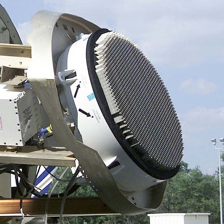
HAPDAR – https://commons.wikimedia.org/wiki/File:HAPDAR_array_installation.jpg
AN/FPS-85 – https://en.wikipedia.org/wiki/Eglin_AFB_Site_C-6
Cobra Dane – https://en.wikipedia.org/wiki/Cobra_Dane
PAVE PAWS – https://en.wikipedia.org/wiki/PAVE_PAWS
AN/SPY-1 – https://missilethreat.csis.org/defsys/an-spy-1-radar/
AN/MPQ-65 – https://en.wikipedia.org/wiki/MIM-104_Patriot
B-1B – http://www.northropgrumman.com/Capabilities/ANAPQ164Radar/Pages/default.aspx
JSTARS – https://en.wikipedia.org/wiki/Northrop_Grumman_E-8_Joint_STARS
F-22 – http://fullafterburner.weebly.com/next-gen-weapons/anapg-77-radar-modes
F-35 – http://www.mwrf.com/systems/radar-systems-make-historyAEHF –
Space Fence – https://www.globalsecurity.org/space/systems/space-fence.htm
IFDL – http://fullafterburner.weebly.com/aerospace/lockheed-f22-raptor-the-definition-of-stealth
MADL – https://www.harris.com/sites/default/files/downloads/solutions/f-35-solutions.pdf
F-35 – http://www.togethertruax.com/#sthash.P6D5bibB.dpbs
DISTRIBUTION A. Approved for public release: distribution unlimited. 22www.darpa.mil DISTRIBUTION A. Approved for public release: distribution unlimited. 23
You can also read