Materials and devices for fundamental quantum science and quantum technologies - Fermilab ...
←
→
Page content transcription
If your browser does not render page correctly, please read the page content below
FERMILAB-PUB-22-046-SQMS

                                                        Materials and devices for fundamental quantum science and quantum technologies
                                                           Marco Polini,1, 2, ∗ Francesco Giazotto,3, † Kin Chung Fong,4 Ioan M. Pop,5, 6 Carsten Schuck,7, 8, 9
                                                            Tommaso Boccali,10 Giovanni Signorelli,10 Massimo D’Elia,1, 10 Robert H. Hadfield,11 Vittorio
                                                               Giovannetti,12 Davide Rossini,1, 10 Alessandro Tredicucci,1, 3 Dmitri K. Efetov,13 Frank
                                                               H. L. Koppens,13, 14 Pablo Jarillo-Herrero,15 Anna Grassellino,16 and Dario Pisignano1, 3
                                                                     1 Dipartimento di Fisica, Università di Pisa, Largo Bruno Pontecorvo 3, I-56127 Pisa, Italy
                                                                        2 Istituto Italiano di Tecnologia, Graphene Labs, Via Morego 30, I-16163 Genova, Italy
                                                                         3 NEST, Istituto Nanoscienze-CNR and Scuola Normale Superiore, I-56127 Pisa, Italy
                                                         4 Quantum Engineering and Computing Group, Raytheon BBN Technologies, Cambridge, Massachusetts 02138, USA
                                                 5 Institute for Quantum Materials and Technology, Karlsruher Institute of Technology, 76344 Eggenstein-Leopoldshafen, Germany
                                                                          6 Physikalisches Institut, Karlsruhe Institute of Technology, 76131 Karlsruhe, Germany
                                                                    7 Institute of Physics, University of Münster, Wilhelm-Klemm-Str. 10, 48149 Münster, Germany
                                                                           8 Center for Nanotechnology (CeNTech), Heisenbergstr. 11, 48149 Münster, Germany
                                                                             9 Center for Soft Nanoscience (SoN), Busso-Peus-Str. 10, 48149 Münster, Germany
                                                                                  10 INFN, Sezione di Pisa, Largo Bruno Pontecorvo 3, I-56127 Pisa, Italy
arXiv:2201.09260v1 [quant-ph] 23 Jan 2022

                                                                  11 James Watt School of Engineering, University of Glasgow, Glasgow G12 8QQ, United Kingdom
                                                                          12 NEST, Scuola Normale Superiore and Istituto Nanoscienze-CNR, I-56127 Pisa, Italy
                                                                      13 ICFO-Institut de Ciències Fotòniques, The Barcelona Institute of Science and Technology,
                                                                                 Av. Carl Friedrich Gauss 3, 08860 Castelldefels (Barcelona), Spain
                                                         14 ICREA-Institució Catalana de Recerca i Estudis Avançats, Passeig Lluı́s Companys 23, 08010 Barcelona, Spain
                                                              15 Department of Physics, Massachusetts Institute of Technology, Cambridge, Massachusetts 02139, USA
                                                                                    16 Superconducting Quantum Materials and Systems Center,
                                                                                Fermi National Accelerator Laboratory, Batavia, Illinois 60510, USA
                                                                                                     (Dated: January 25, 2022)
                                                               Technologies operating on the basis of quantum mechanical laws and resources such as phase coherence
                                                            and entanglement are expected to revolutionize our future. Quantum technologies are often divided into
                                                            four main pillars: computing, simulation, communication, and sensing & metrology. Moreover, a great
                                                            deal of interest is currently also nucleating around energy-related quantum technologies. In this Per-
                                                            spective, we focus on advanced superconducting materials, van der Waals materials, and moiré quantum
                                                            matter, summarizing recent exciting developments and highlighting a wealth of potential applications,
                                                            ranging from high-energy experimental and theoretical physics to quantum materials science and energy
                                                            storage.

                                               Quantum information science, a very active research field              the fabrication of high-quality devices for quantum computa-
                                            stemming from the convergence of quantum mechanics and                    tion, quantum communication, quantum sensing and metrol-
                                            information science that developed towards the end of the                 ogy, and quantum simulation. One of the key elements of this
                                            twentieth century, has led us to a “second quantum revolu-                Perspective is that we treat on equal footing these four pil-
                                            tion” [1–3]. The promised outcome is a portfolio of next-                 lars together with recent progress in quantum thermodynam-
                                            generation quantum technologies that can outperform current               ics, highlighting a number of topics related to the interplay
                                            systems based on the discoveries made during the “first quan-             between quantum mechanical resources and energy/work. We
                                            tum revolution,” such as semiconductor devices and lasers.                focus on materials science discoveries and related devices,
                                               In these present times, the acceleration of the second quan-           which will hopefully yield scalable architectures, in the same
                                            tum revolution is truly tangible. We are currently witnessing             way that the transistor, integrated circuits and magnetic hard
                                            an overwhelming proliferation of sensational headlines about              disks have led to a revolution in computing power, portable
                                            game changing developments in quantum technology. Fur-                    electronics and the ability to store and handle huge amounts
                                            thermore, quantum technology programs are heavily financed                of data. We do not analyze quantum coherent systems such
                                            throughout the globe, from the United States [4] to the United            as cold atoms [8], trapped ions [9], and Rydberg atoms [10],
                                            Kingdom [5], Europe [6], and China [7]. In the midst of                   for which recent Reviews and Perspective articles are already
                                            this global excitement, with scientists urged to raise barri-             available.
                                            cades against marketing zingers, this Perspective has a very
                                            humble and down-to-earth scope. We simply offer an inter-
                                            disciplinary view on recent materials science efforts towards                 I.   SUPERCONDUCTING CAVITIES, QUBITS, AND
                                                                                                                                          MEMORIES

                                            ∗ marco.polini@unipi.it                                                      Superconducting materials are considered key candidates
                                            † francesco.giazotto@sns.it                                               for a number of cutting-edge applications in quantum tech-
                                            This manuscript has been authored by Fermi Research Alliance, LLC under
                                            Contract No. DE-AC02-07CH11359 with the U.S. Department of Energy,
                                            Office of Science, Office of High Energy Physics.
2

                                                                               B.   Disordered superconductors for qubits
nology, particularly in the fields of quantum computation and
radiation sensing. In this Section we summarize the most re-
                                                                        In the last decade several disordered superconducting ma-
cent trends towards the implementation of high-performance
                                                                     terials, such as NbN [21], NbTiN [22], TiN [23], and granular
qubits based on three-dimensional (3D) superconducting cav-
                                                                     aluminum (grAl) [24] have entered the scene and will proba-
ities, disordered and high-Tc superconducting films, and two-
                                                                     bly play an important role in future devices. These materials
dimensional (2D) van der Waals (vdW) materials—see Fig. 1.
                                                                     share at least two valuable attributes for quantum circuits: i)
We then briefly address recent designs for superconducting
                                                                     Disorder in their structure is directly proportional to charac-
memories, which also represent a pivotal asset for the realiza-
                                                                     teristic sheet inductance, enabling the realization of so-called
tion of an energy-efficient superconducting computer.
                                                                     superinductors, inductors with a characteristic impedance ex-
                                                                     ceeding the resistance quantum R0 ≡ h/(4e2 ) ' 6.45 kOhm
                                                                     (where h is Planck’s constant and e is the elementary charge),
                                                                     without the use of mesoscopic Josephson junctions [25]; ii)
                                                                     Thanks to their relatively large London penetration depth,
                                                                     disordered superconductors can withstand in-plane magnetic
                 A.   Superconducting cavities                       fields, allowing them to be used in hybrid circuits to imple-
                                                                     ment couplers, readout resonators, and qubits [26, 27].
                                                                        Due to their complex internal structure, however, disor-
   Substantial progress has been made in the 3D circuit quan-        dered superconductors are in principle more exposed to dis-
tum electrodynamics (cQED) architecture [11–13] whereby              sipation and dephasing mechanisms [28]. Understanding and
coupling between 3D superconducting radio frequency (SRF)            mitigating decoherence mechanisms in homogeneously disor-
cavities and 2D superconducting qubits is achieved. This ar-         dered (NbN, NbTiN, TiN, InO, etc.) and grAl superconduc-
chitecture offers several advantages with respect to conven-         tors is a significant challenge, and it will probably be linked
tional 2D architectures for quantum computing and sensing.           to the exploration of a rich landscape of quantum phenom-
These include: i) A lower surface-to-volume ratio, minimiz-          ena [29].
ing the effect of dielectric losses; ii) A clean electromagnetic
environment, the enclosing superconducting cavity serving as
an effective shield; and iii) The possibility to encode several                     C.   High-Tc superconducting qubits
qubits inside each of the cavity-transmon modules. The latter
allows to substantially decrease the required number of mi-
                                                                        Phase slip nanowires (PSNs), made from high-Tc materials,
crowave channels for system control/manipulation.
                                                                     are promising for novel qubit implementations because they
   Recently, a large leap was achieved at Fermilab in the co-        feature long-lived excited states at temperatures that exceed
herence times of 3D SRF resonators in the quantum regime,            the operating point of most low-Tc devices by 2-3 orders of
reaching lifetimes on the order of 2 s [14]. These were pos-         magnitude.
sible thanks to materials science advancements, in particular           In nanowires made from cuprate superconductors, such as
the abatement of two-level-system (TLS) losses in niobium            yttrium barium copper oxide (YBCO), several quantized en-
via in-situ baking and dissolution of the amorphous niobium          ergy levels of Josephson plasma oscillations can persist due
pentoxide layer. Thanks to this breakthrough, SRF cavities           to the fact that the superconducting energy gap is much larger
are now orders of magnitude more coherent than state-of-             than that of their low-Tc counterparts. Different from tunnel
the-art superconducting qubits, creating a promising approach        Josephson junctions, such PSNs with finite critical current are
to build cavity-based logical qubits where superpositions of         superconducting weak links with direct conductivity and non-
Fock states of the cavity can be engineered to encode a qubit        linear current-phase relations [30, 31].
or even a register. A simple example consists in encoding               For sufficiently small nanowire cross sections and a low
the |0i and |1i states into the presence or absence of mi-           density of Cooper pairs, large fluctuations of the order param-
crowave photons in specific cavity quantum states. This ap-          eter make phase slippage the dominant mechanism for resis-
proach has been pioneered and successfully demonstrated by           tive states [32]. Small nanowire cross sections also transform
several leading groups—see e.g. Refs. [15, 16]—and could             the d-wave symmetry of the order parameter with zero-gap
be used for error correction on qubit registers living in the 2D     nodes into fully gapped states with dramatically reduced num-
Fock space of an SFR cavity [17, 18]. Furthermore, the proof-        bers of quasiparticles at low temperature, thereby yielding
of-concept demonstration of a “random-access” quantum pro-           millisecond-long excited state lifetimes and very high quality
cessor [19] based on controlling a multi-cell 3D cavity with a       factors [33]. Employing current-biased PSNs as qubits that
single transmon opens up a promising pathway for fast scale-         are resilient to charge and critical current noise [34] hence
up via applications of multi-cell high-coherence SRF cavities        provides a perspective for a significant improvement over the
as multi-qubit quantum processor units. The fact that there is       coherence times of current low-temperature superconducting
plenty of room available in the quadrature space of an oscilla-      circuits, thus benefiting the number of executable gate opera-
tor offers a tantalizing, possibly hardware efficient, alternative   tions.
to quantum error correction compared to extended 2D qubit               Progress with high-Tc PSNs will depend on better control
fabrics [20].                                                        over the material properties as well as improving the theoret-
3

ical description of superconducting fluctuation phenomena in                      E.   Superconducting memories
high-Tc systems.
                                                                      Although superconducting processors both in the quantum
                                                                  and classical regimes promise increased computational power,
                                                                  it is recognized that dense arrays of fast memory cells are one
                                                                  of the main limiting factors to achieve a complete supercon-
                                                                  ducting computer.
      D.   Quantum devices built by using vdW materials               As a matter of fact, fast and scalable superconducting mem-
                                                                  ories have not yet been implemented, since their operation
                                                                  typically relies on the inductance of their superconducting
   Advancements in materials research can potentially im-         loop [49], the latter being on the order of a few microm-
prove qubit coherence and functionality. To date, conven-         eters of diameter. In the context of fully-superconducting
tional superconducting qubits are mostly fabricated by using      memories, some improvements were achieved in the last few
amorphous aluminum and its oxide, which can host TLSs,            years by exploiting either Nb-based current-controlled non-
limiting qubit coherence. Several possible paths have been        volatile kinetic inductance memory elements [50, 51] or Al-
recently followed to increase coherence: i) Replacing the ox-     based persistent non-volatile Josephson phase-slips memory
ide [35]; ii) Employing crystalline epitaxial materials such as   cells [52]. Yet, the use of magnetic memories enables minia-
GaAs [36] and nitrides [37, 38]; and iii) Employing 2D vdW        turization down to the nanometer scale, but in such a case hy-
materials [39–43].                                                brid ferromagnet-superconductor elements are exploited. In
                                                                  particular, the operation of either Nb-based Josephson memo-
   Unlike epitaxial materials, vdW crystals are usually           ries containing Ni [53] or PdFe [54] ferromagnetic layers was
grown by chemical vapor deposition/transport or by the flux       recently demonstrated. The realization of Nb-based Joseph-
method [44], before being assembled to a designed het-            son junctions integrated with a magnetic spin valve was also
erostructure by stacking. Scalable growth, transfer and wafer-    reported [55], providing an alternative prototype for a non-
scale integration have become quite mature [45, 46] in the        volatile nanoscale memory device. Very recently, an Al-based
recent years. The vdW materials platform presents an inter-       superconducting, flux-tunable, non-volatile thermal memory
esting case because the weak vdW force between the layers         cell was also reported [56], which could prove its potential for
allows for atomically sharp interfaces despite the lattice mis-   applications in energy harvesting and thermal logic architec-
match and because no chemical bonds form between the lay-         tures [57].
ers. Moreover, the gate tunability of vdW materials can be
useful in modulating quantum devices [39, 41]. Recently,
transmons using vdW parallel-plate capacitors have demon-                II.   QUANTUM COMPUTING APPLICATIONS
strated quantum coherence [42, 43]. To avoid energy relax-
ation of qubits by phonon emission, non-piezoelectric crys-
                                                                    Scientific computing is more and more important in ex-
tals with inversion symmetry are preferred. Research on
                                                                  perimental and theoretical hard sciences, where the need to
piezoelectric devices such as high-overtone bulk acoustic res-
                                                                  process vast amounts of data or perform complex and long
onators (HBAR) and related materials such as LiNbO3 is im-
                                                                  ab-initio calculations increases faster than technology. Quan-
portant though for the realization of quantum transduction and
                                                                  tum Computing (QC) is a candidate solution, at least in the
memories [47].
                                                                  medium-to-long time frame.
   To suppress the loss of quantum information, research for
next-generation qubits will need to focus on low-loss ma-
terials, as measured by the so-called “loss tangent”, which       A.   Computational quantum chemistry and many-body physics
is inversely proportional to the maximum possible T1 relax-
ation time of a qubit. In the microwave frequency range              It is widely believed that QC has the potential to tackle clas-
where superconducting qubits operate, losses increase as the      sically intractable problems in chemistry, physics, and ma-
probe power decreases due to mechanisms involving TLSs            terials science, where electronic structure calculations play a
and quasiparticles. The maximal loss when the probe power         key role [58]. In fact, due to the increasing ambition to sim-
corresponds to a single photon is most relevant to qubit relax-   ulate complicated chemical compounds, chemical processes
ation because qubits operate in the single-photon regime. This    (e.g. in electrochemical batteries) and quantum materials, and
aspect highlights the need for materials research under the       to identify molecules that exhibit significant therapeutic ac-
very challenging conditions of low signal and low-noise en-       tivity against a disease, electronic structure calculations are
vironment. As discussed above, higher superconducting tran-       becoming more and more computationally expensive. The
sition temperatures are also desirable because a larger super-    aim is to find the eigenstates and corresponding eigenvalues
conducting gap may suppress quasiparticle generation, which       of an electronic Hamiltonian, including electron-electron (e-e)
is often a dominant mechanism of qubit relaxation. New con-       interactions. For example, in computational quantum chem-
cepts, such as merged-element transmons [48] and gate tun-        istry one needs to deal, for a given nuclear configuration, with
able qubits [41], critically demand for materials development.    an electronic Hamiltonian describing electrons in a molecule,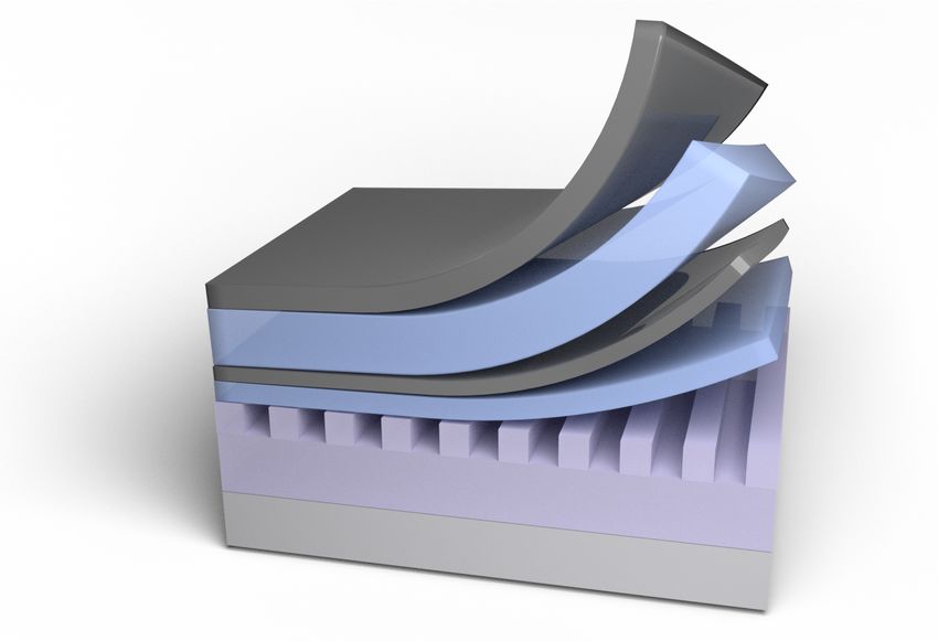
4

                                                                         Memories
                   SRF cavities                                               Al, Nb
                        Nb

                                                                                                                                 SNSPDs
                                                                                                           NbN, NbTiN, MoGe, MoRe, NbRe, TaN, NbSi, MoSi, WSi, MgB2

                                                                                                                                      Magnetometers
                                                                                                                                         (SQUID)
                                                                                                                                             Nb, YBCO

                      1mK              10mK                  100mK                     1K                  10K                100K           Temperature

                                                                                                                                 Qubits
                                                                                                                                   YBCO

                                                                              MKIDs, TESs
                                                                      Al, W, MoAu, Nb, Ti/Al, NbN, NbTiN

                                             Qubits
                                  Al, grAl, Nb, InO, Ta, NbN, NbTiN

FIG. 1. Superconducting quantum devices for quantum technologies and their operating temperature ranges. Top left panel: A
Nb SRF cavity for, e.g., dark axion searches. Top central panel: Pseudo-color scanning electron micrograph of a prototypical persistent
Josephson phase-slip memory cell (PSMC) with topological protection. The inset shows a blow-up of the PSMC in the Josephson weak-link
region (green nanowire). The color legend indicates the material used for each circuit element: yellow and green for aluminum, and red
for AlMn-Ox. The PSMC has been operated from 25 mK up to about 1K. Adapted from Ref. [52] under the terms of the CC 4.0 license
(http://creativecommons.org/licenses/by/4.0). Bottom left panel: Scanning electron micrograph image of a fluxonium qubit built by using a
granular Al (grAl) superinductor. The qubit consists of a Josephson junction shunted by a 300-µm-long grAl superinductor, and it is coupled
through a shared inductance LS to a microwave resonator consisting also of a grAl inductor Lr and a coplanar capacitor. The color legend
indicates the material used for each circuit element: blue for aluminum, red for grAl and purple for aluminum covered with grAl. Adapted
by permission from Ref. [25]. Copyright © Springer Nature (2019). Bottom right panel (courtesy of Matvey Lyatti, University of Münster,
Germany): Scanning electron micrograph of a YBCO phase-slip nanowire (PSN) produced by focused ion beam milling. The large intrinsic
capacitance C between the direct current-carrying (orange) PSN and the superconducting electrodes is required to readout the nanowire
quantum state. We have also plotted typical spatial fluctuations of the order parameter |Ψ| along the nanowire. Regions where |Ψ| is strongly
suppressed are akin to dynamical Josephson weak links. Scale bar: 500 nm. List of acronyms present in the figure: SRF = Superconducting
Radio Frequency; SNSPDs = Superconducting Nanowire Single-Photon Detectors; SQUID = Superconducting Quantum Interference Device;
Qubits = Quantum bits; MKIDs = Microwave Kinetic Inductance Detectors; TESs = Transition Edge Sensors.

                                                                                            Wigner [59] and Bravyi-Kitaev encodings [60]. After the
interacting with the nuclei and among each other. Solving                                   mapping has been carried out, a quantum algorithm needs to
the corresponding Schrödinger equation for a range of nu-                                  be used for finding the ground and excited states of the chem-
clear configurations yields the potential energy surfaces of the                            ical/physical system of interest. Examples include the vari-
molecule. Mapping out these potential energy curves explic-                                 ational quantum eigensolver (VQE) [61] and quantum phase
itly is exponentially costly in the number of degrees of free-                              estimation [62, 63]. Finally, one needs to use suitable tech-
dom of the molecule. In condensed matter physics and materi-                                niques to mitigate the effects of noise in non-error-corrected
als science, instead, one typically deals with crystals featuring                           QC platforms (such as Google “Sycamore”, IBM Quantum
Bloch translational invariance and a given number of atoms                                  “System One”, Rigetti “Aspen”, “Zuchongzhi”, etc), which
per unit cell. When the single-particle Bloch bands are narrow                              will be crucial for achieving accurate simulations. Indeed, it
or flat (as in the case of the moiré quantum materials discussed                           is to date under debate and a topic of research whether or not
below in Sect. V), e-e interactions lead to strong correlations,                            such noisy intermediate-scale quantum (NISQ) devices [64]
which are difficult to tackle analytically or numerically.                                  will be able to solve classically-intractable problems of chem-
   A QC approach starts by encoding first- or second-                                       ical and physical interest.
quantized fermionic Hamiltonians of chemical and physical                                      Recently, Arute et al. [65] have implemented a VQE on the
interest onto a collection of qubits. An encoding method is                                 Google Sycamore superconducting quantum processor using
a map from the fermionic Fock space to the Hilbert space of                                 up to 12 qubits. More precisely, the experiment implements
qubits such that every fermionic state can be represented by                                the mean-field Hartree-Fock method for calculating the bind-
a qubit state. Several different encoding protocols are avail-                              ing energy of hydrogen chains and the isomerization of di-
able. For example, second-quantized fermionic Hamiltonians                                  azene. While it is totally feasible to solve the exact same
can be mapped onto qubit Hamiltonians by using the Jordan-                                  problem on a classical computer, this work demonstrates sev-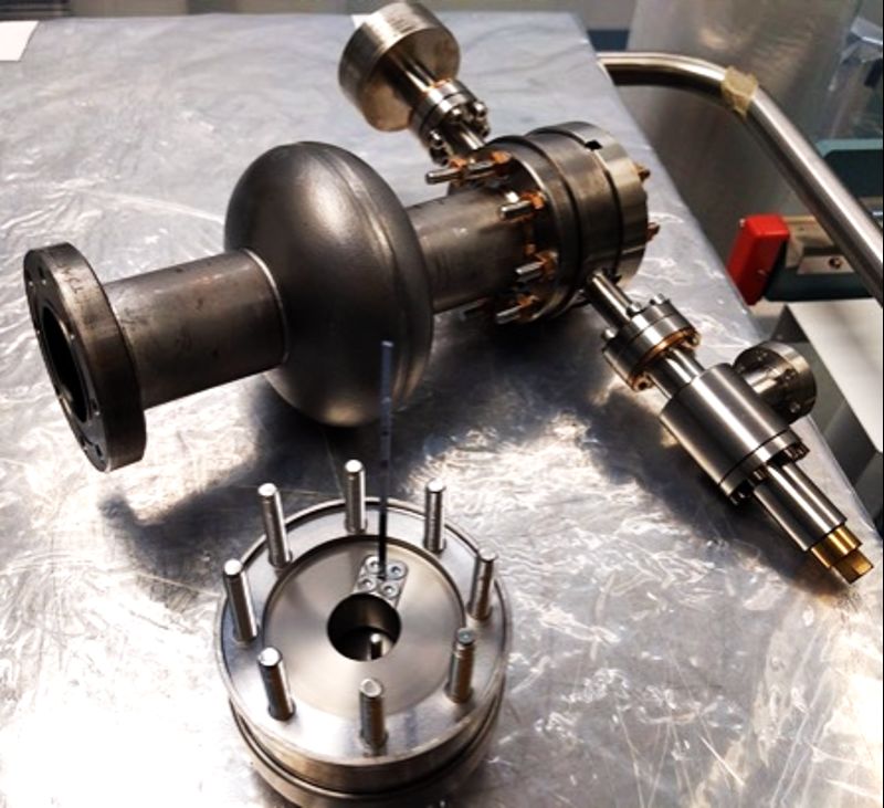
5

eral key building blocks for quantum chemistry simulations             In this respect, a quantum computer would represent the
and paves the way for achieving quantum advantage for prob-         ideal solution to the problem [71], as originally envisioned by
lems of chemical interest. We refer the reader to the excellent     Richard Feynman. Indeed, the sign problem is not an intrinsic
recent review by McArdle et al. [58] for more details on com-       problem of the physical system by itself, but just a wrong but
putational quantum chemistry and an exhaustive list of refer-       compelling choice of the computational basis on a classical
ences.                                                              computer. A quantum computer would ideally be able to ex-
   In the realm of many-body physics and in view of their           plore the space of quantum states of the system, e.g. through
limited size and coherence, it seems wise in the short term         a quantum Markov chain [72, 73] or by other suitable algo-
to identify particular physical phenomena that NISQ devices         rithms [74, 75], so as to provide us with the information we
can immediately and naturally realize, as opposed to physics        are presently missing.
they could realize universally. For example, Ippoliti et al. [66]      In perspective, realistic applications would need to digital-
have demonstrated that the architecture of Google Sycamore          ize a 3D lattice with at least ten sites in each direction, with
is ideal to realize an elusive non-equilibrium state of matter,     fermion fields living on each site and an SU(3) gauge link
i.e. the so-called “discrete time crystal” [67]. Another possible   variable for each site and direction. The number of required
near-term application of NISQ devices is to analyze quantum         qubits, considering also error correction issues, largely ex-
critical systems [68, 69]. The collective behavior of a quantum     ceeds those that can be realistically predicted for real quantum
many-body system near a quantum phase transition (QPT)              machines in the next few years. The road for algorithmic and
can be described, both at and out-of equilibrium conditions         technological development is however open now.
induced by unitary or dissipative mechanisms, via a unified
scaling picture that may hold in the thermodynamic and finite-
size scaling limits [68]. For continuous QPTs such framework
is based on the renormalization-group theory of critical phe-
nomena, while in the case of first-order quantum transitions it
                                                                         C.   Data analysis in high-energy physics experiments
is ruled by the avoided crossing of two levels, being character-
ized by an extreme sensitivity to the boundary conditions. The
emerging scenario is amenable to direct laboratory testing in          In the last three decades, high-energy physics (HEP) experi-
available NISQ devices as e.g. finite-size scaling emerges in       mental and theoretical sectors have increasingly become more
small-sized systems, with a few tens of lattice sites [68]. To      computing hungry, with needs that have largely surpassed a
mention a concrete example, the critical properties of the one-     “constant cost envelope”, even in presence of very effective
dimensional (1D) quantum Ising model have been probed on            technological improvements from the vendors [76]. The next
a Rigetti (Aspen-9) superconducting quantum processor via a         big jump in resource needs is expected to happen when the
Kibble-Zurek process (a dynamically-driven phenomenon to            High Luminosity Large Hadron Collider (LHC) [77] will en-
access quantum criticality), obtaining scaling laws and esti-       ter operations, around 2028. Current estimates indicate that
mating critical exponents despite inherent sources of errors        the cost of computing will be up to three times the amount of
on the hardware [69].                                               money spent yearly at the present [78].
                                                                       QC is potentially one of the groundbreaking technologies
                                                                    that can drastically change the picture, in both experimental
            B.   Computational high-energy physics                  and theoretical HEP. Possible solutions have been sketched in
                                                                    a series of recent papers, which show the power of QC in ar-
   The Standard Model of particle physics is based on quan-         eas including computationally heavy algorithms [79, 80], im-
tum gauge theories. Its predictions affect a wide range of          proved selection of physics signatures [81–83] and more effi-
phenomena, ranging from the physics of the early universe           cient and precise theoretical modelling [84]. In general, QC
to hadron phenomenology. In some cases, like e.g. in the            seems the natural solution to substitute heavily combinatorial
case of low-energy quantum chromodynamics (QCD), they               algorithms, like those used in track finding in silicon devices
can only be obtained by numerical means. Lattice QCD sim-           and in the clustering of deeply segmented calorimeter signals.
ulations have been representing a major challenge for high          On top of this, the availability of large dimension minimiza-
performance computing in the past few decades. They usu-            tion systems, as those from adiabatic annealing machines, can
ally proceed through a Monte Carlo sampling of the QCD              serve as a drop-in replacement for multiple reconstruction and
path integral, a task which is feasible on a classical com-         analysis algorithms, based on χ 2 or likelihood minimization.
puter, even if requiring resources close to the exascale. How-      The same tool would be the holy grail if applicable to ma-
ever, in some conditions, like for QCD at finite baryon den-        chine learning training [85]. QC algorithms could in princi-
sity or for non-equilibrium phenomena, the approach fails, be-      ple be usable in online systems, for example in the discrim-
cause the path integral measure becomes complex and Monte-          ination between useful and background events (the so-called
Carlo methods are not applicable. This is the (in)famous “sign      “trigger”). On top of the problems described above, their im-
problem”, which has similar counterparts in condensed mat-          plementations have presently to cope with the bottleneck of
ter physics [70], and strongly limits our present knowledge,        the time-consuming preparation of the initial state and hence
for instance about neutron star physics.                            seem futuristic [81].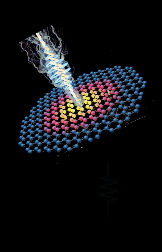
6
a) b)
c)
LETTERS NATURE NANOTECHNOLOGY
d) a
Top mirror Gaussian beam
NA = 0.28
b
e) 10 9
Mirror pairs
8 7 6 5 f)
1.0
–4 –2 0 2 4
0.9
x (µm)
Efficiency 0.8
0.7 β
κtop/(κ + γ)
0.6
κtop/(κ + γ) β
κopt
•
0.5
101 102
H κ/2π (GHz)
z V
c
(x,y) QD Vg
H-mode
V-mode
QD Intra-cavity pulse
Intensity
Laser pulse
Bottom mirror
xyz nano-positioner
–100 –50 0 50 100 150
∆ν (GHz)
Fig. 1 | Concept of the single-photon source. a, The semiconductor heterostructure consists of a GaAs/AlAs Bragg mirror, the bottom mirror and a p–i–n
diode. The InGaAs quantum dots (QDs) are located in the intrinsic region, in tunnel contact with the Fermi sea in the n layer. An electric voltage (Vg) is
FIG. 2. Quantum communications. The past decade has seen huge interest in ambitious quantum key distribution (QKD) implementations
applied between the p and the n regions of the diode. The position of the heterostructure can be adjusted (↔, ↕) with respect to the top mirror, a concave
mirror in a silica substrate, using an xyz nano-positioner. A simulation (red points) shows that the output is very close to a Gaussian beam (black line,
and has spurred the development of quantum devices and platforms. Panel a) Handheld QKD transmitter (courtesy of Dominic O’Brien, joint
R2!=!99.95%). NA, numerical aperture. b, Calculated conversion efficiency of a quantum dot exciton to photon exiting the top mirror, as a function of
the decay rate through the top mirror κtop for ‘atom’–photon coupling g/(2π)!=!4.3!GHz, atom decay rate γ/(2π)!=!0.30!GHz and rate of unwanted loss
κloss/(2π)!=!0.72!GHz. The efficiency η is given by η!=!κtop/(κ!+!γ)!×!β (with κ!=!κtop!+!κloss); β!=!FP/(FP!+!1) with FP!=!4g2/(κγ). The number of mirror pairs refers
work of University of Bristol & University of Oxford, UK quantum communications hub, United Kingdom). Panel b) Satellite QKD linking
to the top mirror. c, Excitation scheme. The quantum dot is in resonance with the H-polarized microcavity mode; the laser is blue-detuned and V-polarized.
The driving intensity as experienced by the quantum dot is shown. Δν, detuning from the quantum dot.
to long distance fiberlossesoptic networks [102, 122] (courtesy of Jian-Wei Pan, University of Science and Technology of China). Adapted by
reduce the Q-factor only for r ≲ 6 μm. At the radius of curva- birefringence arising mostly from some residual uniaxial strain in
used here, r =I 12 μm, the calculated Q-factor is 99% of the Q the semiconductor (Supplementary Information Section III); the
permission from Ref.ture [102].
-factor Copyright
in the large-r limit. I
These simulations ©up Springer
back Nature
the experi-I spectrum of the laser pulses(2017). Panel
is larger than this splitting (Fig. 1c). c)
The Chip-to-chip QKD with integrated photonics [106]. Adapted
mental result that κ is small. With the highly reflective top mir- quantum dot is tuned into resonance with the higher-frequency,
from Ref. [106] under the
ror, the terms of
quantum-dot/cavity systemthe
loss
enters CC
the strong4.0 license
coupling H-polarized (http://creativecommons.org/licenses/by/4.0).
mode. The laser is V-polarized and blue-detuned with
regime of cavity-quantum electrodynamics , allowing a precise respect to both microcavity modes such that the tails of the laser
7
Panel d) High efficiency semiconductor
of the coupling, g/(2π) = 4.3 GHz. In the experiments spectrum and the V-polarized microcavity mode overlap at the
quantum dot coherentmeasurement
single-photon
reported emitter
here, we use a modest reflectivity [94]. Adapted
top mirror (transmission by permission
frequency of the H-polarized mode (Fig. 1c). The quantum from dot Ref. [94]. Copyright © Springer Nature (2021). Panel e) QKD
10,300 ppm per round trip, according to the design) chosen such emits preferentially into the H-polarized microcavity mode. The
receiver with waveguide integrated
that κ lies close superconducting
to the efficiency maximum nanowire
(Fig. 1b). The measured cross-polarized scheme (suppressionsingle-photon
10 for pulsed excitation) now detectors (SNSPDs) (courtesy of Robin Terhaar, University of
Q-factor is 12,600 (κ/(2π) = 25.92 GHz), matching closely the value separates the V-polarized laser pulses from the H-polarized single
6
Münster, Germany). expected
Panel
I
f) Ultra low jitter SNSPD [103]. Adapted by permission from Ref. [103]. Copyright © Springer Nature (2020).
from the design of the two mirrors in the large-r limit photons with a loss depending only on the unwanted coupling of the
(Supplementary Information Section V). This analysis shows that quantum dot to the V-polarized mode (Supplementary Information
κloss/(κ + γ) ≈ 3%. Section V). Provided that the mode splitting is larger than the mode
The semiconductor heterostructure contains thin n- and p-type linewidths13, this loss is small.
layers with the quantum dots in tunnel contact with the n-type We choose a quantum dot and maximize the coupling of the X+
layer such that a Coulomb blockade is established (Supplementary resonance to the microcavity. To do this, we record a decay curve
Information Section I). Contacts to the n- and p-type layers are following resonant excitation: the radiative decay rate is largest at
made at the edge of the chip, far from the microcavity itself. The maximum coupling. The quantum dot and microcavity frequencies
chip is positioned relative to the top mirror in situ (Fig. 1a).
A challenge in all optically driven quantum dot single-photon
are tuned to establish a resonance (Fig. 2a). The Purcell factor FP
is determined by scanning the microcavity frequency: on resonance
ties to boost the rate of information transmission above the
sources is to separate the single-photon output from the driving laser with a microcavity mode, the decay time is 47.5 ps; far detuned, the
light. A standard scheme is to excite and detect in a cross-polarized
configuration. Applied to a charged exciton for which the transi-
decay time tends to 520 ps, resulting in FP = 10 for quantum dot
number one (QD1), and FP = 12 for quantum dot six (QD6) (Fig. 2b).
threshold one would assign to a transmission line by purely
tions are circularly polarized, this scheme leads to a 50% loss in On resonance with the H-polarized microcavity mode, we deter-
the collection efficiency. Here, we avoid this loss by exploiting the
mode splitting in the microcavity13. We work with the positively
mine βH, the probability of emission into the H-polarized mode, to
be βH = 86% (Fig. 2b and Supplementary Information Section V).
classical considerations; finally, the quantum key distribution
charged exciton, X+, which has circularly polarized transitions (σ+
III. QUANTUM COMMUNICATION
for hole spin-⇓, σ− for hole spin-⇑). The microcavity mode splits
We now maximize the flux of single photons. Implementing the
excitation scheme (Fig. 1c), the central frequency of the laser is tuned (QKD) algorithm, which instead enables distant users to dis-
into two modes, horizontally-polarized and vertically-polarized to find the maximum signal. As a function of laser power, the quan-
(H- and V-polarized), separated by 50 GHz, on account of a small tum dot signal exhibits oscillations, indicative of Rabi oscillations till a common private key to be employed for the encryp-
400 NATURE NANOTECHNOLOGY | VOL 16 | APRIL 2021 | 399–403 | www.nature.com/naturenanotechnology
Quantum communication (Fig. 2) is arguably one of the tion of messages [90], by carefully exploiting coherent super-
most mature sectors of quantum technology. Progress has positions of input signals that travel over a public line (possi-
been advanced by extensive collaborations across academia bly monitored by eavesdroppers).
and industry. Quantum communication deals with the pos- Quantum communication has been a major driver for re-
sibility of exploiting effects such as entanglement, squeez- search into novel quantum devices. Considering the canonical
ing, and, more generally, coherent superpositions of quantum QKD link between Alice and Bob over fiber or free space [91],
states, to improve signaling processes between distant parties there are several main components. The source (Alice), the
both in terms of transmission efficiency and security [86]. The link, and the detector (Bob). The source may comprise a solid
overarching goal of quantum communication is the realization state laser attenuated to the single photon level, photon pair
of an augmented version of the current global communica- sources [92] or single photon emitters (such as semiconductor
tion network (the quantum secure communication network) quantum dots [93, 94] or diamond NV centres [95] or defects
that would enable one to incorporate some of the most ex- in 2D materials [96, 97]). 2D materials are very appealing for
otic, yet effective protocols ever conceived in quantum infor- on-chip quantum devices for quantum integrated photonic cir-
mation theory. These include the quantum teleportation algo- cuits, because of the ease and low-cost of integration with the
rithm [87] which, by exploiting pre-shared entanglement be- Si and SiN photonic platforms, and because emitters, modu-
tween the sender and the receiver enables them to efficiently lators, and detectors are all based on the same material plat-
exchange the quantum state of a quantum memory, effectively form [98, 99].
overcoming the limit imposed by the no-cloning theorem [88]; The link can comprise low loss optical fibers or free space
the superdense coding algorithm [89] which, again by exploit- (in the atmosphere, space, or underwater). QKD schemes
ing pre-shared entanglement, allows the communicating par- commonly rely on single photon detectors [100]. For free
7

                                                                        A. Superconducting nanowire single-photon detectors,
                                                                       transition edge sensors, and microwave kinetic inductance
space QKD, including recent space-to-ground QKD demon-                                          detectors
strations [101, 102], photon counters such as Si single-photon
avalanche diodes (SPADs) are the common choice in the 600-
900 nm wavelength range. The optimal transmission window               In the near-infrared regime, superconducting single-photon
for optical fibers is 1550 nm (losses as low as 0.15 dB per km      detectors (SPD), such as SNSPDs (see Sect. III), transition
in silica fibers) spurring development of InGaAs SPADs or           edge sensors (TESs), and microwave kinetic inductance de-
low noise, low jitter superconducting nanowire single-photon        tectors (MKIDs) have been key building blocks for quantum
detectors (SNSPDs) [103, 104]. Recently transmission at             technologies, i.e. for revolutionary free-space quantum com-
longer (mid-infrared) wavelengths has been considered, for          munication protocols [122]. Popular choices of materials for
satellite or photonic crystal fiber QKD [105]. As QKD ar-           these detectors include [123] Al, Nb, MoSi, WSi, NbN, and
chitectures become more mature and ambitious, there are re-         NbTiN. Further studies on the details of the underlying detec-
quirements for materials development in other related areas:        tion mechanisms and superconductor properties [124, 125] are
integrated photonics for on-chip QKD [106–110], hybrid on-          shedding light on how to optimize the performance of these
chip integration, random number generators based on quan-           detectors. For example, they will teach us how to operate at
tum devices, high-performance low-loss interconnects, mod-          higher temperatures, i.e. by capitalizing on the recent efforts
ulators, filters and switches, quantum memories and repeaters.      employing materials like MgB2 , bismuth strontium calcium
A major imperative for wider rollout of quantum communica-          copper oxide (BSCCO), and YBCO [33, 126], or at lower pho-
tions is the threat to conventional public key encryption meth-     ton energies, i.e. in the mid- and far-infrared spectral regions,
ods (such as the RSA algorithm [111]) posed by the near-            where the number of quasiparticles generated by a single pho-
term realization of practical quantum computers capable of          ton decreases.
implementing powerful factorization algorithms [112]. Sen-
sitive governmental, financial or personal data from past or
future communications is under threat of capture and decryp-
tion. We anticipate there will be increasing demand for mass
produced secure quantum communications platforms for sce-
narios such as satellite-to-ground communications, handheld                                B.   vdW sensors
devices, fiber optic networks and future data centres. There-
fore, there is little doubt quantum communication is likely to         In the new frontier of single-photon detection in the THz
remain a catalyst for quantum device research for the coming        and microwave regimes, vdW materials are emerging as a
decades.                                                            promising platform for quantum sensing [127]. These materi-
                                                                    als can be only one or a few atomic layers thick, with ultrahigh
                                                                    photoconductive gain [128] and minute thermal conductance,
                                                                    resulting in a relatively large bolometric temperature rise upon
                                                                    photon absorption. Specifically, for graphene, its electron heat
                                                                    capacity can be vanishingly small near the charge neutrality
       IV.     QUANTUM SENSING PLATFORMS AND                        point due to its pseudo-relativistic band structure. By over-
             INTERDISCIPLINARY APPLICATIONS
                                                                    coming the challenge of photon coupling and thermal readout
                                                                    based on the Josephson effect [129], it has been demonstrated
   Exploiting their sensitivity to the external environment,        that the sensitivity of graphene bolometers can reach the fun-
quantum sensors can outperform detectors that rely on clas-         damental limits imposed by thermal fluctuations [130], suit-
sical principles alone [113] (see Fig. 3). Examples such as su-     able for quantum circuits [131]. Single-photon detection of
perconducting interference devices, atomic systems, and NV          near-infrared photons has recently been demonstrated using a
centers in diamond [114–117] have demonstrated how quan-            graphene-based Josephson junction [129]. Due to graphene’s
tum phenomena can achieve unprecedented sensitivities in            capability of coupling to electromagnetic waves in a wide
measuring time, electric, and magnetic fields.                      range of frequencies, the fast thermalization time of its car-
                                                                    riers, and its ultrafast response, graphene-based detectors rep-
   More recently, quantum sensing is becoming more inter-           resent an attractive solution for broadband quantum sensing,
disciplinary with applications going well beyond quantum in-        provided that device fabrication will be improved and made
formation science and traditional areas of condensed matter         scalable.
physics. An exciting frontier is that of applications to as-
troparticle physics, i.e. to the search of dark matter axions via      Finally, as we will discuss in Sect. V, we highlight that
magnetic topological insulators [118], Josephson parametric         moiré superconductors created in vdW heterostructures offer
amplifiers [119, 120], and superconducting qubits [121].            interesting opportunities for quantum sensing. Indeed, these
                                                                    systems have large kinetic inductances that can be useful for
   Materials research will continue to advance quantum sens-        the development of MKIDs or TESs [132], since the super-
ing by improving coherence and suppressing losses, as well as       conducting carrier density can be lower than conventional su-
to expand applications to a broader range.                          perconductors by 5 orders of magnitude.
8

          a)                                                                                                                                                                                                                                                                                                                                                                                                                                                                                                                                                                                                                                                                                                                                                                                                                                                                                                                                                                                                                                                                        b)           c)
                                                                                                                                                                                                                                                                                                                                                                                                                                                                                                                                            photon

                                                                                                                                                                                                                                                                                                                                                                                                                                                                                                                                                     graphene

                                                                                                                                                                                                                                                                                                                                                                                                                                                                                                                                                                                                                                                                                                                                                                                                                                                                                                                                                                                                                                                                                    e)           d)
               Ce                                                                                                                                                                                                                                                                                                                                                                                                                                                                                                                                       Rth
               sha1_base64="DksNXFSBmjZbb8xcBYNXDurYPTc=">AAAB8HicbVBNS8NAEJ3Ur1q/qh69LBbBU0lE1GOxF48V7Ie0oWy2k3bpbhJ2N0IJ/RVePCji1Z/jzX/jts1BWx8MPN6bYWZekAiujet+O4W19Y3NreJ2aWd3b/+gfHjU0nGqGDZZLGLVCahGwSNsGm4EdhKFVAYC28G4PvPbT6g0j6MHM0nQl3QY8ZAzaqz0WO9nPSUJTvvlilt15yCrxMtJBXI0+uWv3iBmqcTIMEG17npuYvyMKsOZwGmpl2pMKBvTIXYtjahE7Wfzg6fkzCoDEsbKVmTIXP09kVGp9UQGtlNSM9LL3kz8z+umJrzxMx4lqcGILRaFqSAmJrPvyYArZEZMLKFMcXsrYSOqKDM2o5INwVt+eZW0LqreVfXy/rJSu83jKMIJnMI5eHANNbiDBjSBgYRneIU3RzkvzrvzsWgtOPnMMfyB8/kDfHSQNw==
               AAAB8XicbVBNS8NAEJ3Ur1q/qh69LBbBU0lE1GPRi8cq9gPbUDbbTbt0swm7E6GE/gsvHhTx6r/x5r9x2+agrQ8GHu/NMDMvSKQw6LrfTmFldW19o7hZ2tre2d0r7x80TZxqxhsslrFuB9RwKRRvoEDJ24nmNAokbwWjm6nfeuLaiFg94DjhfkQHSoSCUbTS430v6+qI4HDSK1fcqjsDWSZeTiqQo94rf3X7MUsjrpBJakzHcxP0M6pRMMknpW5qeELZiA54x1JFI278bHbxhJxYpU/CWNtSSGbq74mMRsaMo8B2RhSHZtGbiv95nRTDKz8TKkmRKzZfFKaSYEym75O+0JyhHFtCmRb2VsKGVFOGNqSSDcFbfHmZNM+q3kX1/O68UrvO4yjCERzDKXhwCTW4hTo0gIGCZ3iFN8c4L8678zFvLTj5zCH8gfP5A3B5kMc=
9

                                                                   candidates for the accurate investigation of these strongly cor-
at the part per trillion level. The coherence of the quantum de-   related quantum phases. For example, the onset of a quantum
vices employed in this class of experiments is a critical factor   spin liquid phase of the paradigmatic toric code [144] type
in determining the sensitivity of the particle search or prop-     was detected in 2D arrays of 219 87 Rb atoms individually
erty measurement. Important materials advancements and re-         trapped in optical tweezers and positioned on the links of a
search directions include coating these 3D structures with thin    kagome lattice [145]. Similarly, toric code states have been
films of superconductors, such as Nb3 Sn, NbTi or higher-Tc        prepared and analyzed by using a quantum circuit compris-
materials such as rare-earth barium copper oxide (also known       ing 31 superconducting qubits [20]. While these systems are
as ReBCO), that minimize microwave losses in the presence          highly controllable and can faithfully realize certain quantum
of high magnetic fields [136, 137], since the presence of a        Hamiltonians, engineering tunable long-range interactions re-
large magnetic field (up to several Teslas) will increase the      mains an outstanding experimental challenge. For example,
discovery potential of the experiments.                            two atoms in Rydberg states interact with each other through
                                                                   a vdW potential decaying like the inverse sixth power of the
                                                                   relative distance. On the contrary, the relevant e-e interaction
             D.   New device concepts and designs                  potential in solids decays like the inverse first power of the
                                                                   relative distance (Coulomb law). The quantum simulation of
   Some novel superconducting platforms for sensing have           a plethora of strongly correlated phases of matter therefore
been envisioned and experimentally realized in the last            requires controllable and ultra-clean quantum many-particle
few years. Among them, one original approach is to ex-             systems interacting through Coulomb forces.
ploit the principle of temperature-to-phase [138] conversion,         In this respect, a breakthrough is represented by the discov-
which is based on the exploitation of superconductor/normal        ery of correlated insulators and superconductivity in magic-
metal/superconductor DC proximity SQUIDs. Here, absorp-            angle twisted bilayer graphene [146, 147]. These findings
tion of radiation yields heating of one of the two junctions       have led to the emergence of a new platform, which has been
of the SQUID, thereby inducing a change of the phase drop          dubbed moiré quantum matter [148] (MQM), to investigate
across the other junction, which is detected via a tunnel probe    strongly correlated and topological physics of 2D electron
connected to it—see Fig. 3d).                                      systems (see Fig. 4). MQM refers to long-wavelength su-
   Other alternative device concepts rely on the use of ferro-     perlattices obtained by stacking or rotating relatively to each
magnetic insulators-based superconducting tunnel junctions         other two or more 2D crystals such as graphene, hexagonal
exploiting, for instance, thin EuS layers coupled to the su-       boron nitride, and transition metal dichalcogenides. A peri-
perconductor so as to induce a sizable thermoelectric effect       odic modulation of the inter-layer electron hopping in these
in the structure [139]. Heating one part of the junction due       stacks leads to band flattening [149] (bandwidth of the flat
to radiation absorption translates into a thermovoltage output     bands on the order of 10-20 meV), which, in turn, results into
signal, which can then be detected. Still in the context of su-    strong correlations (on-site Hubbard interaction energy scale
perconducting tunnel junctions, a single-photon thermal de-        on the order of 50-100 meV).
tector operating in the dissipationless regime, and based on          The MQM platform has led to unprecedented electrical
the sharp jump of the critical current of a temperature-biased     control over multiple phases of matter in 2D material het-
tunnel junction has been proposed [140].                           erostructures. Unraveling the exact microscopic mechanisms
   Recently, an Al-based quantum capacitance detector [141],       that are responsible for superconducting phases in MQM is
where photon-excited quasiparticles tunnel into a Coulom-          currently one of the biggest challenges in the field. In these
bic island embedded in a resonant circuit, displayed an ultra-     systems, superconductivity is believed to be unconventional,
low noise-equivalent power (NEP) below 10−20 W/Hz1/2               as it often arises in the presence of strong electronic corre-
at 1.5 THz. Finally, a prototype for a Josephson escape            lations [147] or close to magnetically ordered states [150].
sensor (JES) consisting of a fully superconducting 1D Al-          In magic-angle twisted trilayer graphene [151, 152] the su-
based Josephson junction was also demonstrated [142]—see           perconducting phase has been explicitly shown to violate the
Fig. 3e). The JES is expected to yield thermal fluctuation         Pauli limit [153], which likely points towards a spin-triplet
noise-limited NEP around 10−25 W/Hz1/2 if operated as a            Cooper pairing. The experimental exploration of collective
bolometer, and a frequency resolution of about 2 GHz when          modes in these materials is still at its infancy [154]. As sam-
operated as a calorimeter.                                         ple quality increases and tools like cryogenic near-field optical
                                                                   spectroscopy [155, 156] become more and more developed,
                                                                   several new types of collective excitations are expected to be
 V.   SOLID-STATE QUANTUM SIMULATORS BASED ON                      discovered and linked with broken symmetry phases of MQM.
              MOIRÉ QUANTUM MATTER                                   Since MQM is made from stacks of 2D materials, it pos-
                                                                   sesses revolutionary tuning parameters that can be used a)
   Interactions between matter constituents, such as electrons     to accurately control interaction energy scales and symme-
in a crystal, are the source of some of the most fascinating       tries for the simulation of fundamental physics problems [157]
states of matter, such as strange metals, exotic superconduc-      and b) to enable entirely new device concepts for quantum
tors, and topologically-ordered phases with fractionalized ex-     technologies. As far as point a) is concerned, for example,
citations. Programmable quantum simulators [143] are ideal         inter-layer alignment between the various layers can be used
10

                                                                    (see Sect. II). Obvious and timely directions here are those
                                                                    related to the increase of the performance of electrochemical
to alter symmetries and band widths [158]. Metallic elec-           batteries. An example is that of scientists from IBM and Mit-
trodes (i.e. gates) can be used to control the electron filling     subishi Chemical, who have simulated on a NISQ device the
via the electric field effect and alter the range of e-e interac-   initial steps of the reaction mechanism between lithium and
tions via screening [159]. With respect to point b), we mention     oxygen in lithium-air batteries [183, 184].
for example “hyper-tunable” Josephson junctions [160, 161]
                                                                       But clearly there is much more than that. How can quan-
(where both the superconductor and weak link are realized
                                                                    tum mechanics help breakthroughs in energy technology? We
within the same moiré material and they are both electri-
                                                                    foresee three possible groundbreaking directions.
cally tunable) and exquisitely sensitive quantum photodetec-
tors [132, 162, 163], with unprecedented capabilities to de-           a) First, solid-state devices whose functionalities are en-
tect single photons in the Terahertz and microwave regimes.         abled by quantum mechanical resources such as entanglement
A series of important steps have to be made by the com-             and coherence [57, 185, 186] will play a much broader role
munity, though, to make sure that MQM becomes an estab-             in the future. Indeed, it is difficult to imagine a “quantum
lished platform for quantum simulation. First, twist-angle in-      society” where computing, communications, and sensing will
homogeneities [164] have to be tamed. Second, new meth-             be carried out by relying on the principles of quantum me-
ods to assemble and nanofabricate MQM on large scales are           chanical laws while energy will be provided by systems ruled
needed. While some robotic and machine-learning enhanced            by standard electrochemical laws and 200-years old designs.
automated fabrication methods for 2D materials have been de-        There are three classes of energy-related quantum devices,
veloped recently [165, 166], substantial efforts are needed to      which are currently being mainly studied by academia and
extend them to precisely controlled moiré heterostructures and     that will need to gradually be evaluated and adopted by indus-
to achieve large-scale fabrication capabilities.                    try: i) quantum heat engines for energy production [187–194],
                                                                    ii) quantum batteries [195–205] and supercapacitors [206] for
   An alternative approach to realize MQM consists in placing
                                                                    energy storage, and iii) quantum energy lines [207] for energy
single- or few-layer graphene over a dielectric [167] or metal-
                                                                    transfer. Research and development on all these aspects may
lic [168] substrate which has been patterned. Such periodic
                                                                    lead to a profound “cultural” and technological revolution in
spatial modulations can lead to a synthetic version of MQM
                                                                    how energy is produced, stored, and conveyed.
that is in principle more versatile than the “natural” MQM
discussed above, with freedom to choose crystal symmetry,              b) Second, we believe that also cavity quantum electrody-
synthetic strain, etc. Replica Dirac cones, Hofstadter butterfly    namical control of the ground and excited states of molecu-
spectra, and anisotropic electron transport have already been       lar systems and quantum phase transitions of extended elec-
demonstrated via patterning techniques [169–171]. The holy          tron systems [208, 209] may play an important role in the en-
grail of synthetic MQM is to realize highly tunable flat elec-      ergy sector. When electromagnetic fields are confined to a
tronic bands [172] such that strong e-e interactions can be in-     cavity, vacuum fluctuations are greatly enhanced and are ex-
duced. This enables the exploration of correlated phenomena         pected to alter the properties of a variety of quantum systems.
such as superconductivity and magnetism with a highly con-          Experimentally, it has been shown for example that the vac-
trollable system.                                                   uum field can favor a particular product in transformations of
                                                                    compounds that have two or more reactive sites, provided that
                                                                    vibrational strong coupling between a reactant and the vac-
                                                                    uum field of an optical cavity is achieved [210]. Experimental
  VI.   QUANTUM TECHNOLOGIES FOR THE ENERGY                         evidence of the impact of vacuum fields on superconducting
                    SECTOR                                          compounds [211] and 2D electron gas physics [212] has also
                                                                    been reported. If and how quantum fluctuations of cavity elec-
   A great deal of interest is currently also nucleating around     tromagnetic fields will play a pivotal role in energy-related
quantum technologies for the energy sector [173, 174]. Many         issues is certainly an interesting research direction. For exam-
researchers in the past decade have studied the impact of quan-     ple, strong coupling between electronic degrees of freedom
tum effects on a variety of devices and systems (including bio-     and the vacuum field has been shown to lead to a large in-
logical and bio-artificial ones) for the harvest and transmission   crease in the capacitance of a quantum supercapacitor [206].
of energy. For example, quantum coherence and interference             c) Third, quantum mechanics can also help to develop green
effects have been proposed as means to suppress charge re-          quantum technologies. For example, qubit driving schemes
combination losses and enhance the efficiency of photovoltaic       that reuse and correct drive pulses can help reduce the av-
devices [175, 176] as well as to increase the yield of pho-         erage energy consumption per gate operation in a quantum
tosynthetic architectures [177, 178]. Similarly, several au-        computer, without increasing the average gate error [213]. In-
thors have discussed the possibility to boost the performance       genious QC schemes where energy is recycled from one com-
of organic photovoltaic cells by relying on long-range energy       putational step to the next have also been proposed [214]. Fi-
transfer between organic molecules enabled by vacuum-field          nally, constraints on the physical resources for quantum com-
cavity polaritons [179–182]. Nowadays, however, the first           putation have been shown [215] to lead to a maximum prob-
thing that comes to mind, when the words “quantum” and “en-         ability that an error occurs in a physical gate or qubit that
ergy” are mentioned together, is probably applications of QC        grows as the scale of the quantum computer grows. Energy
to computational quantum chemistry and materials science            minimization constraints are an obviously important resource
You can also read