Microscopic metallic air-bridge arrays for connecting quantum devices
←
→
Page content transcription
If your browser does not render page correctly, please read the page content below
Microscopic metallic air-bridge arrays for connecting quantum devices
                                                                 Y. Jin,1 M. Moreno,2, a) P. M. T. Vianez,1, a) W. K. Tan,1 J. P. Griffiths,1 I. Farrer,3 D. A. Ritchie,1 and C. J. B.
                                                                 Ford1, b)
                                                                 1)
                                                                    Semiconductor Physics Group, Department of Physics, Cavendish Laboratory, University of Cambridge, Cambridge,
                                                                 CB3 0HE, UK
                                                                 2)
                                                                    Departamento de Fı́sica Aplicada, Universidad de Salamanca, Plaza de la Merced s/n, 37008 Salamanca,
                                                                 Spain
                                                                 3)
                                                                    Department of Electronic & Electrical Engineering, University of Sheffield, Sheffield, S1 3JD,
                                                                 UK
                                                                 (Dated: 12 February 2021)
arXiv:2102.06123v1 [cond-mat.mes-hall] 11 Feb 2021

                                                                 We present a single-exposure fabrication technique for a very large array of microscopic air-bridges using a
                                                                 tri-layer resist process with electron-beam lithography. The technique is capable of forming air-bridges with
                                                                 strong metal-metal or metal-substrate connections. This was demonstrated by its application in an electron
                                                                 tunnelling device consisting of 400 identical surface gates for defining quantum wires, where the air-bridges
                                                                 are used as suspended connections for the surface gates. This technique enables us to create a large array of
                                                                 uniform one-dimensional channels that are open at both ends. In this article, we outline the details of the
                                                                 fabrication process, together with a study and the solution of the challenges present in the development of
                                                                 the technique, which includes the use of water-IPA developer, calibration of resist thickness and numerical
                                                                 simulation of the development.

                                                        The successful interconnection of conducting layers is              An alternative approach is variable exposure: the
                                                     key to the performance of printed or integrated circuits.           electron-beam penetration depth into the resist can be
                                                     When fabricating ultra-small specialised research devices           controlled by varying the acceleration voltage and dose on
                                                     however, the process for depositing and patterning an               a single layer of PMMA resist in a one-stage exposure,10
                                                     insulating layer to keep regions apart, or to space gates           and polyimide and double-layer PMMA can be combined
                                                     away from the surface in places, is complex and often af-           in a two-stage technique.11 In the former method, varying
                                                     fects operation. A straightforward and reliable method              the acceleration voltage has the undesirable consequence
                                                     for bridging between regions is therefore highly desirable          of changing the focus and alignment and the low accel-
                                                     and can make possible much more complicated device                  eration voltage limits the electron-beam resolution. The
                                                     architectures for physics research. This is particularly            latter method does not suffer from these drawbacks but
                                                     needed in areas such as quantum computing, where in-                does involve the use of two lithography stages.
                                                     terconnecting qubits can often prove challenging.                      In this letter, we present a process with the combined
                                                        Normal1 and cross-linked2,3 polymer resist (PMMA)                advantages of the single-stage exposure and multiple-
                                                     has been used as a patterned insulator under metal                  resist methods, in order to fabricate large numbers of
                                                     bridges for studying quantum ring structures and anti-              fine-feature air-bridges with very high yield. We have
                                                     dots. Air-bridges have also been used in quantum-dot in-            optimized the process by using a water/IPA mixture to
                                                     terference devices.4–6 In all these cases, the bridge played        develop the PMMA. This minimizes residual resist and
                                                     a crucial role in connecting a central gate while leaving           gives good exposure contrast. We show results from a
                                                     the interference path undisturbed. Various methods have             set of 1D wires defined using an array of gates linked by
                                                     been employed for the fabrication of these bridges: Li,             ∼ 400 air-bridges. We note however that we have regu-
                                                     Chen, and Chou 7 , for example, demonstrated a process              larly used this technique to fabricate devices with up to
                                                     with nanoimprint lithography (NIL) for monolithic mi-               ∼ 6000 bridges. This technique can also be used to fabri-
                                                     crowave integrated circuits with air-bridges. While NIL             cate bridges up to at least 10 µm in length and therefore
                                                     simplifies repeated fabrication, its complexity is unsuit-          should be useful in a wide range of nanodevices made for
                                                     able for rapid iteration of research prototypes. Instead,           research purposes.
                                                     resist exposure is preferable. Photo-resist can be par-                The development of our air-bridge technique was mo-
                                                     tially cross-linked and later removed to form an air gap            tivated by the need to fabricate arrays of 1D chan-
                                                     below the bridge.8 One drawback of cross-linking, how-              nels in order to study the exotic properties of electron-
                                                     ever, is that it is susceptible to pattern distortion due           electron interactions.12–15 Figure 1a demonstrates the ge-
                                                     to swelling of the resist,9 hence making it unsuitable for          ometry of the array under scanning electron microscopy
                                                     dense sub-micron patterns.                                          (SEM). The substrate is a GaAs/AlGaAs heterostructure
                                                                                                                         that contains two parallel quantum wells separated by
                                                                                                                         a 14 nm-thick tunnel barrier, which allows electron tun-
                                                                                                                         nelling. A 1D electron channel is formed underneath the
                                                     a) These
                                                            authors have contributed equally to this work.               narrow region between each pair of metallic gates when
                                                     b) Author to whom correspondence should be addressed:               they are negatively biased. Each device consists of a large
                                                     cjbf@cam.ac.uk                                                      number of identical channels organized into multiple sets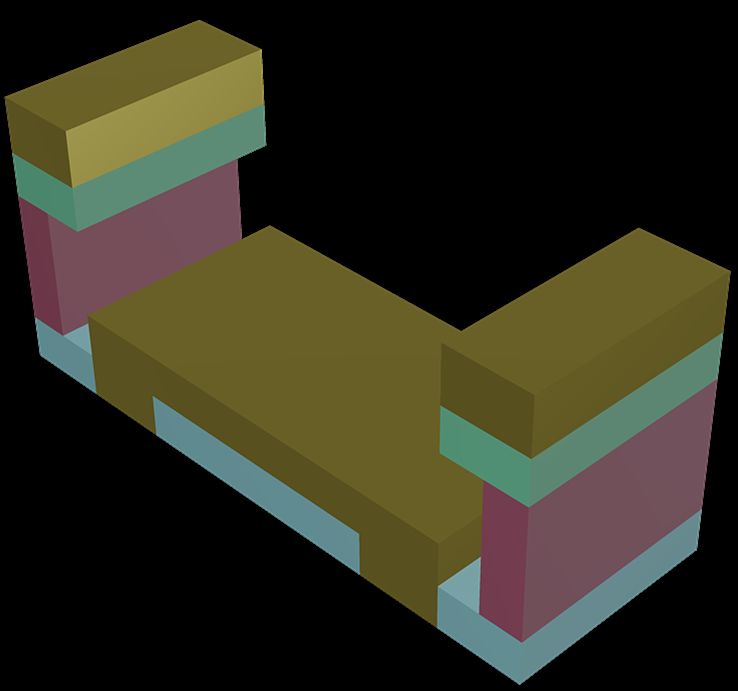
2

(a)                                                  (b)                                   (c)
                                                                        PMMA 100k

                                                                                                            Bridge dose

                                                                 Co-polymer

                                                                                           Pedestal
                                                           PMMA 950k
                                                                                           dose
                                                     (d)                 Gate metal        (e)

FIG. 1. (a) SEM images of a 1D tunnelling device. 1D channels are formed beneath the narrow regions between two depletion
gates. The tunnel device contains multiple columns of identical depletion gates that are inter-connected by air-bridges without
closing the channels, as well as crossing over other device structures. Inset: SEM micrograph of a bridge 10 µm long. (b)–(e)
Air-bridge fabrication by our three-layer PMMA single-exposure process: (b) Triple-layer resist spin-coated on sample surface.
(c) Selective exposure by electron beam and development. Regions exposed to pedestal dose are completely cleared after
development while regions exposed to bridge dose have the 950k layer intact. (d) Gate metallization by thermal evaporation.
(e) Lift-off leaves just the air-bridge pattern.

of parallel wires to enhance the tunnelling current. We          950k PMMA has much lower sensitivity than the other
require the gates to be electrically connected while keep-       resists. The resist profile after development is shown in
ing the potential in the 1D channel as uniform as possible       Figure 1c, where areas exposed by Dp have been com-
along its whole length. Consequently, bridges are neces-         pletely cleared and those exposed by Db are still covered
sary. An air gap, instead of a solid dielectric, provides        in 950k PMMA. The copolymer is far more sensitive than
minimal capacitive coupling between the bridge and the           the PMMA and so the middle layer is undercut relative
2D electron gas (2DEG) in the quantum well underneath,           to the top layer, which aids with the removal of residual
for a given gap height. Approximating the structure to           metal during lift-off. An air-bridge structure is formed
a parallel-plate capacitor, the capacitance is given by          when gate metal is evaporated on top (Figure 1d) and
C = ε0 A/(dsp /εsp + dsub /εsub ), where A is the area of        remains on the sample after the resists are stripped off
the bridge, εsp , εsub are the dielectric constants of the       (lift-off, Figure 1e). Metal over the Dp region is in di-
spacer below the bridge and of the substrate above the           rect contact with the substrate, and is referred to as the
2DEG, respectively, and dsp , dsub are their thicknesses.        pedestal. ‘Bridge‘ regions exposed at Db are covered in
Therefore, C is minimized by minimizing εsp (using an            metal separated from the substrate by an air gap but an-
air gap), and maximizing dsp .                                   chored to the substrate via pedestals. The thickness of
                                                                 the bottom layer of resist after development corresponds
   Figure 1b-1e outlines the steps of our multilayer-            to the height of the air gap below the bridge, which in
resist/single-exposure air-bridge process. It begins with        our samples is approximately ∼ 100 nm.
the spin coating of the sample with three different re-
sist layers, firstly PMMA with molecular weight 950k,              In order to achieve a reliable process, it is necessary
then MMA(8.5)MAA copolymer and finally 100k PMMA                 to precisely control the thickness and uniformity of the
(Figure 1b). Next, the sample is patterned by electron-          resists. Using ellipsometry, we calibrated the thickness
beam lithography (EBL) using two well calibrated doses           as a function of spinner rotation speed for each type of
Dp and Db , referred to as the pedestal dose and the             resist using test wafers. Additionally, after each layer was
bridge dose, respectively. Dp is capable of fully exposing       spin-coated on the actual sample, an ellipsometry mea-
all three resist layers, while Db is only able to expose the     surement was performed to confirm that the resist was
top two and leaves the bottom layer unaffected, because          within ±10 nm of the target thickness. For the reported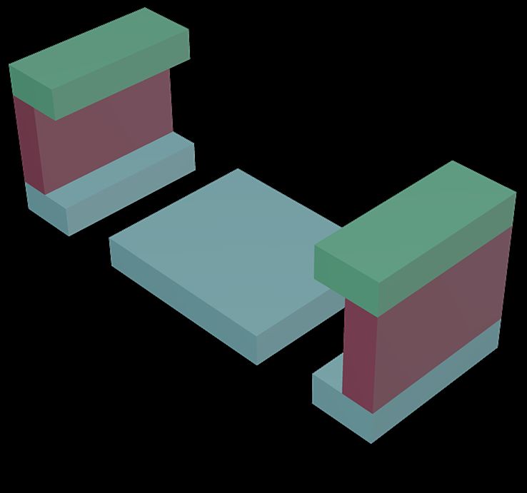
3

                                                                 and the underlying material. For our device this meant
                                                                 the metal-to-metal contact between the pedestals and the
                                                                 1D channel gates. The standard development technique
                                                                 with 3 : 1 MIBK:IPA (isopropanol) developer was found
                                                                 to be unreliable as the resulting air-bridges often broke
                                                                 away from the sample during lift-off. Atomic force mi-
                                                                 croscopy (AFM) showed the cause of this type of fail-
                                                                 ure to be trace amounts of residual resist after devel-
                                                                 opment. Figure 2 shows a comparison of AFM scans
                                                                 of the same exposure pattern on 950k PMMA treated
                                                                 by different developers. The EBL doses and develop-
                                                                 ment times used in these results were such that the sub-
                                                                 strate was expected to be fully exposed after develop-
                                                                 ment. The images demonstrate that the choice of devel-
                                                                 oper has substantial impact on the surface roughness of
                                                                 the developed region. As is shown in Figure 2(b), the
                                                                 surface roughness can be reduced by RF plasma ashing,
                                                                 suggesting these are resist residues. Since plasma ash-
                                                                 ing attacks both the residue and the unexposed resist, it
                                                                 may also cause damage to the ultra-fine resist patterns.
                                                                 The safer option is therefore to adopt the developer that
                                                                 leaves the least amount of resist residue after develop-
                                                                 ment. The use of water/IPA mixture to develop PMMA
                                                                 was studied by Yasin.16,17 Owing to the high sensitivity
                                                                 of the water/IPA developer at room temperature, we con-
FIG. 2. Differentiated AFM images of resists treated by var-     ducted the development at (5.0 ± 0.5) °C with the use of
ious development methods: (a) Three layers of resist (100k,      temperature-controlled water bath, in order to limit the
copolymer, 950k) developed at room temperature (∼ 21 °C)         rate of development and increase the tolerance to timing
for 30 seconds in 3:1 IPA/MIBK. (b) The same sample as           error in the process. The lower temperature also results
in (a) after 15 seconds of plasma ashing at 50 W. (c, d)         in higher contrast.17 The samples were immersed in pre-
Two layers of resist (copolymer, 950k) developed at room
                                                                 cooled beakers of water/IPA mixture with manual agita-
temperature for 5 seconds in (c) 3:7 water-IPA and (d)
3:1:1.5% IPA/MIBK/MEK (methyl ethyl ketone). Corre-              tion. No rinse was used at the end of development, as
sponding cross-sections of the resist height along lines 1 and   immersing the sample in pure water or IPA after devel-
2 are shown above or below each image.                           opment can increase the development rate and was also
                                                                 found to deposit precipitates on the sample surface. The
                                                                 best result was produced when the samples were removed
sample, we applied 133 nm of 950k, 297 nm of copolymer           immediately from the developer and dried with nitrogen
and 128 nm of 100k resists using 60-second spins at 5700,        gas.
4500 and 6000 RPM, respectively. The target thicknesses             In order to calibrate Dp and Db for the triple-layer
were 130, 300 and 130 nm. We note, however, that the             process, we determined the sensitivity curves of the three
thickness can be changed and successful samples have             types of EBL resist by measuring the depths of developed
been obtained within ± 20 % of these values after ad-            resist as functions of electron-beam dose. Measurements
justing for the e-beam dose. The dilution ratios of the          were made on 200 × 300 µm2 rectangular test patterns,
resist solutions were: 4% (w/w) 950k PMMA in anisole             as well as fine gratings with 2 µm width and 2 µm sepa-
diluted with methyl isobutyl ketone (MIBK) in 2:1 vol-           rations. Both types of patterns were exposed with 100 kV
ume ratio, 9% (w/w) copolymer in ethyl lactate and 100k          acceleration voltage on a Vistec VB6 system over a range
PMMA (undiluted). The base doses received by the re-             of doses. The development depth was measured both by
sist for the exposure of the pedestals and bridges were 880      a Dektak surface profiler and an AFM, with the former
and 600 µC/cm2 , respectively Prior to the resists being         method applied to the rectangular patterns and the lat-
applied, the sample was baked on a 150 °C hotplate for           ter to the fine gratings. Figure 3 shows the normalized
10 minutes to eliminate moisture. After each layer was           development depth of different types of resist as func-
applied, the sample was also further baked on a 110 °C           tions of EBL dose. When dose is plotted on logarithmic
hotplate for 10 minutes to dry off solvents in the resist.       scale, the negative of the gradient of the linear part of the
Finally, we note that when spinning, particularly for the        curve is the contrast γ.9 We note that the contrast mea-
100k resist, significantly better uniformity was obtained        sured in our calibration is similar to the values reported
when using a metal as opposed to a PTFE stage.                   by Rooks.18 A polynomial fit to each of these curves was
   The most significant challenge of the air-bridge pro-         used to estimate the rate of development at any arbitrary
cess is achieving good adhesion between the pedestals            dose. To give insight into the development process, we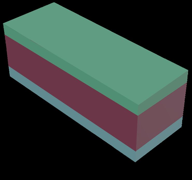
4

                                                                                                                   D=880       D=600          D=880
                                     1                                                                             G=1563      G=1045         G=1563
                                                                                                            0
  Normalised depth of development
                                                                                                                                                          100k
                                                                                                                                                         150 nm
                                    0.8

                                                                                             Depth (nm)
                                                                                                          200
                                                                                                                                                        Copolymer
                                    0.6                                                                                                                  300 nm
                                           Copolymer AFM                                                  400
                                           Copolymer Dektak                       =7.34                                                                   950k
                                    0.4    100k AFM                                                                                                      100 nm
                                                                    =4.52     =6.39
                                           100k Dektak                                                    600
                                           495k AFM                                                         -200   0   200     400      600    800     1000   1200
                                                                            =5.91
                                    0.2    495k Dektak                                                                       Lateral position (nm)
                                           950k AFM
                                           950k Dektak
                                     0
                                     100             200      300      400     500 600 700
                                                                        2
                                                  E-beam dose ( C/cm )

FIG. 3. Contrast curves of different EBL resists based on
development depth after 30 seconds of immersion at 5 °C in 3:7
water/IPA. Each data series is normalized to the undeveloped
thickness of the corresponding type of resist (here, 146 nm for
950k, 313 nm for copolymer and 105 nm for 100k resists). The
contrast γ refers to the gradient of the linear region of the
                                                                                             FIG. 4. Results of a numerical model estimating the evolution
curve.
                                                                                             of resist profile as a function of electron-beam dose and time.
                                                                                             Each contour differs from its closest neighbour by 5 seconds
                                                                                             in development time. The figures at the top of each region are
have developed a numerical model of the process with                                         the average EBL dose D required there, and the actual dose
the electron-beam dose and development time as input.                                        G given by the EBL machine after correcting for proximity-
Our calculation assumes: 1. the development is a time-                                       effect. The same spreading parameters were used in both the
limited process, meaning development depth is always                                         model calculation and the proximity correction. Inset: SEM
proportional to time; 2. the development has a uniform                                       micrograph of an under-developed sample showing a similar
                                                                                             hump of copolymer as predicted by our model.
rate as a function of dose, and is estimated from the con-
trast curve; 3. the direction of development at each point
is normal to the surface there. Figure 4 shows the result
of this numerical calculation by displaying the evolution                                    stage as this was found to often result in damage to the
of the resist profile in 5-second increments. The calcu-                                     bridges.
lation gives a similar hump of copolymer as seen in an                                          We checked the integrity of the newly-fabricated air-
under-developed sample shown in the SEM image in the                                         bridge arrays by inspecting the sample under an opti-
inset.                                                                                       cal microscope. Except for sacrificial trial samples, we
   Calculations performed using the average development                                      refrained from analysing any experimental device under
rates from the measurements in Figure 3 imply that the                                       SEM, so as to avoid potential contamination by electron-
optimum development time should be around 35 s. How-                                         beam-induced deposition. Although individual elements
ever, we found empirically that 60 s–70 s was required to                                    of the array cannot be clearly resolved under an optical
fully develop the combined layers, with poor metal ad-                                       microscope, the large number of repeating units produces
hesion for development times at or below 55 s. This dis-                                     a uniform and iridescent appearance of the entire struc-
crepancy is likely caused by variations in the rate as de-                                   ture. In practice, optical inspection can therefore easily
velopment progresses: solute builds up in the developer,                                     reveal defects in the two EBL layers, with the most com-
slowing down the dissolution. Hence different structures                                     mon modes of failure being incomplete lift-off after the
or depths may require different development times. Prac-                                     base layer metallisation, and poor adhesion between the
tically however, this can be managed by dividing samples                                     air-bridge pedestals and the underlying base-layer metal.
into multiple development batches and using an iterative                                     Both types of failure lead to defects that distort the uni-
scheme to home in on the optimum time for a particular                                       form appearance of the array and are easily visible un-
sample or type of device.                                                                    der optical microscopy. After optical inspection, samples
   After development, we evaporated approximately 110–                                       were tested further for electrical continuity between con-
130 nm (i.e. roughly equal to the thickness of the base                                      tacts. We also checked that the air-bridge-connected wire
resist) of gold at a rate of ∼ 0.3 nm/s. The samples were                                    gates did not short to other nearby control gates.
then left overnight in a bottle of acetone, followed by a                                       Finally, we present some typical measurements of one
water bath at 45 °C for approximately 90min before final                                     of our air-bridge devices. Details of the sample layout
lift-off. Use of ultrasonication is not recommended at this                                  and experimental setup can be found elsewhere.13–15 Fig-
5
(a) (b)
dG/dVDC (μS/mV)
dG/dVWG (μS/V) 0.4
-0.3 Background
2D band (subtracted)
15
-0.35 5
Wire gate voltage VWG (V)
3rd sb
10 0.2
2nd sb 2D system
-0.4
5
VDC (mV)
1st sb
0 0
-0.45 0
-5
-0.5 1D system
-5 -0.2
-10
-0.55
-15
-0.6 -0.4
0 1 2 3 4 5 0 1 2 3 4 5
Magnetic field B (T) Magnetic field B (T)
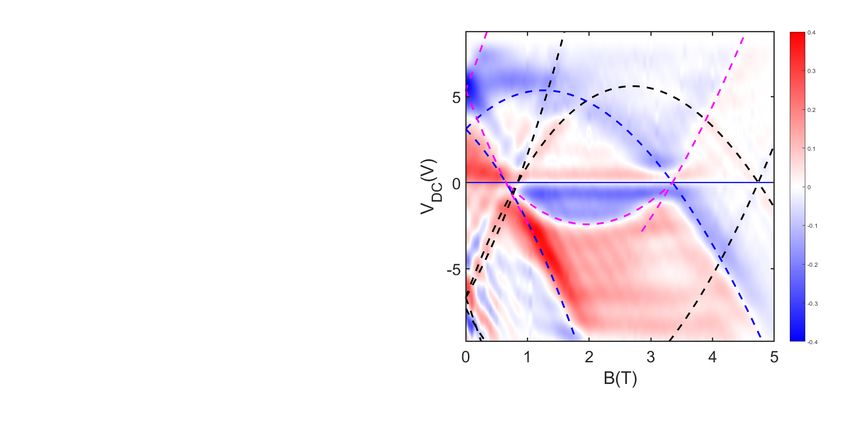
FIG. 5. (a) Derivative of the equilibrium tunneling conductance G of the resonance device with respect to the 1D wire-gate
voltage VWG vs magnetic field B and VWG , at T = 0.3 K and normalised along B. The black dashed curves mark the 2D band
and the 1D subbands. Three 1D subbands can be resolved, with the last subband cutting off at VWG ∼ −0.55 V. (b) Tunnelling
differential dG/dVDC vs B and the DC bias VDC between the two quantum wells, with VWG held at −0.515 V. The parabolae
indicate the positions of the calculated dispersions of the 1D subbands. At this wire-gate voltage, only a single 1D subband is
observed. The magenta/blue parabolae mark the observed dispersions resulting from 1D-2D tunnelling. The black parabolae
correspond to the dispersions of the background ‘parasitic‘ tunnelling region.
ure 5a shows an intensity map of the equilibrium tun- in a single step of EBL exposure. The essential steps
nelling conductance (i. e. at zero DC bias VDC between to the process are: 1. Careful control of the thickness of
the wells) between the two quantum wells of the device deposited resist; 2. Accurate calibration of the dose curve;
as a function of the in-plane magnetic field B and the 3. Use of a water/IPA developer to improve the adhesion
1D wire-gate voltage VWG . The dashed lines highlight of the air-bridge pedestals. The process is suitable for
the positions of the local maxima of the tunnelling con- fast iteration of prototype or research devices and can be
ductance. Figure 5b shows the tunnelling conductance generalised to other substrate materials and metals.
differential dG/dVDC measured in terms of B and VDC Acknowledgements: The authors would like to thank
between the wells, while the 1D wire gates are held at Yunchul Chung (Pusan National University, South
−0.515 V. For an electron to tunnel between the quan- Korea) for advice on air-bridge fabrication. This
tum wells, the difference in energy between its initial and work was supported by the UK EPSRC [Grant Nos.
final states must be provided by eVDC , and the canoni- EP/J01690X/1 and EP/J016888/1]. P.M.T.V. ac-
cal momentum boosted by the Lorentz force, ∝ B. The knowledges financial support from EPSRC Interna-
maximum conductance is therefore observed when the tional Doctoral Scholars studentship via grant number
Fermi energy and wavevector of one (2D) system tracks EP/N509620/1.
the dispersion of the other (1D) system, revealing the dis-
persions of the electron subbands, which are found to be
essentially parabolic. Detailed fitting of these dispersions DATA AVAILABILITY
reveals the existence of strong electron-electron interac-
tions in the 1D wires, including separate spin and charge
The data and modelling code that support this work
modes. Since G is summed over the ∼ 400 1D channels in
are available at the University of Cambridge data repos-
a single device, the fact that that we are able to resolve
itory.
the 1D subband structure clearly (Fig. 5a) demonstrates
the high degree of uniformity of the wire-gate array, and 1 C. J. B. Ford, T. J. Thornton, R. Newbury, M. Pepper,
that the air-bridge structure connecting the gate array H. Ahmed, D. C. Peacock, D. A. Ritchie, J. E. F. Frost, and
performs reliably. G. A. C. Jones, Appl. Phys. Lett. 54, 21 (1989).
2 I. Zailer, J. E. F. Frost, V. Chabasseur-Molyneux, C. J. B. Ford,
In conclusion, we have demonstrated a process that is M. Pepper, D. A. Ritchie, and G. A. C. Jones, Semicond. Sci.
capable of reliably fabricating large arrays of air-bridges Tech. 11, 1235 (1996).6 3 M. Kataoka, C. J. B. Ford, M. Y. Simmons, and D. A. Ritchie, 12 M. Moreno, C. J. B. Ford, Y. Jin, J. P. Griffiths, I. Farrer, Phys. Rev. Lett. 89, 226803 (2002). G. A. C. Jones, D. A. Ritchie, O. Tsyplyatyev, and A. J. 4 A. Yacoby, M. Heiblum, V. Umansky, H. Shtrikman, and D. Ma- Schofield, Nature Communications 7, 12784 EP (2016). halu, Phys. Rev. Lett. 73, 3149 (1994). 13 O. Tsyplyatyev, A. J. Schofield, Y. Jin, M. Moreno, W. K. Tan, 5 Y. Ji, Y. Chung, D. Sprinzak, M. Heiblum, D. Mahalu, and A. S. Anirban, C. J. B. Ford, J. P. Griffiths, I. Farrer, G. A. C. H. Shtrikman, Nature 422, 415 (2003). Jones, and D. A. Ritchie, Phys. Rev. B 93, 075147 (2016). 6 I. Gurman, R. Sabo, M. Heiblum, V. Umansky, and D. Mahalu, 14 O. Tsyplyatyev, A. J. Schofield, Y. Jin, M. Moreno, W. K. Tan, Phys. Rev. B 93, 121412 (2016). C. J. B. Ford, J. P. Griffiths, I. Farrer, G. A. C. Jones, and D. A. 7 M. Li, L. Chen, and S. Y. Chou, Applied Physics Letters 78, Ritchie, Phys. Rev. Lett. 114, 196401 (2015). 3322 (2001). 15 Y. Jin, O. Tsyplyatyev, M. Moreno, A. Anthore, W. K. Tan, J. P. 8 S. Jie, Journal of Microelectromechanical Systems 21, 1285 Griffiths, I. Farrer, D. A. Ritchie, L. I. Glazman, A. J. Schofield, (2012). and C. J. B. Ford, Nature Communications 10, 2821 (2019). 9 G. Brewer, in Electron-Beam Technology in Microelectronic Fab- 16 S. Yasin, D. G. Hasko, and H. Ahmed, Applied Physics Letters rication (Academic Press, 1980). 78, 2760 (2001). 10 E. Girgis, J. Liu, and M. L. Benkhedar, Applied Physics Letters 17 S. Yasin, D. Hasko, and H. Ahmed, Microelectronic Engineering 88, 202103 (2006). 6162, 745 (2002). 11 A. Khalid, C. Li, J. Grant, S. Saha, S. Ferguson, and D. R. 18 M. J. Rooks, Journal of Vacuum Science Technology B: Micro- Cumming, Microelectronic Engineering 98, 262 (2012). electronics and Nanometer Structures 20, 2937 (2002).
You can also read