Monolithic 3D-based SRAM/MRAM Hybrid Memory for an Energy-efficient Unified L2 TLB-Cache Architecture - ResearchGate
←
→
Page content transcription
If your browser does not render page correctly, please read the page content below
This article has been accepted for publication in a future issue of this journal, but has not been fully edited. Content may change prior to final publication. Citation information: DOI
                                                                            10.1109/ACCESS.2021.3054021, IEEE Access

Date of publication xxxx 00, 0000, date of current version xxxx 00, 0000.
Digital Object Identifier 10.1109/ACCESS.2020.Doi Number

Monolithic 3D-based SRAM/MRAM Hybrid
Memory for an Energy-efficient Unified L2 TLB-
Cache Architecture
Young-Ho Gong1, Member, IEEE
1
 School of Computer and Information Engineering, Kwangwoon University, Seoul Republic of Korea (email: yhgong@kw.ac.kr)
Corresponding author: Young-Ho gong (e-mail: yhgong@kw.ac.kr).
The present research has been conducted by the Research Grant of Kwangwoon University in 2020. This work was also supported by the National Research
Foundation of Korea (NRF) grant funded by the Korea government (MSIT) (No. NRF-2020R1G1A1100040)

ABSTRACT Monolithic 3D (M3D) integration has been emerged as a promising technology for fine-
grained 3D stacking. As the M3D integration offers extremely small dimension of via in a nanometer-scale,
it is beneficial for small microarchitectural blocks such as caches, register files, translation look-aside
buffers (TLBs), etc. However, since the M3D integration requires low-temperature process for stacked
layers, it causes lower performance for stacked transistors compared to the conventional 2D process. In
contrast, non-volatile memory (NVM) such as magnetic RAM (MRAM) is originally fabricated at a low
temperature, which enables the M3D integration without performance degradation. In this paper, we
propose an energy-efficient unified L2 TLB-cache architecture exploiting M3D-based SRAM/MRAM
hybrid memory. Since the M3D-based SRAM/MRAM hybrid memory consumes much smaller energy than
the conventional 2D SRAM-only memory and 2D SRAM/MRAM hybrid memory, while providing
comparable performance, our proposed architecture improves energy efficiency significantly. Especially, as
our proposed architecture changes the memory partitioning of the unified L2 TLB-cache depending on the
L2 cache miss rate, it maximizes the energy efficiency for parallel workloads suffering extremely high L2
cache miss rate. According to our analysis using PARSEC benchmark applications, our proposed
architecture reduces the energy consumption of L2 TLB+L2 cache by up to 97.7% (53.6% on average),
compared to the baseline with the 2D SRAM-only memory, with negligible impact on performance.
Furthermore, our proposed technique reduces the memory access energy consumption by up to 32.8%
(10.9% on average), by reducing memory accesses due to TLB misses.

INDEX TERMS Monolithic 3D, Cache memory, Translation look-aside buffer, SRAM, MRAM, Energy
efficiency

I. INTRODUCTION                                                                                      HBM), it is not appropriate for finer-grained 3D integration
   As process technology shrinks, microprocessor                                                     (e.g., 3D stacking of small caches) due to the micrometer-
performance has been significantly improved. However,                                                scale dimension of TSVs; though Intel adopts TSV-3D in
with the technology scaling down to sub-10nm node, the                                               their recent commercial processor [9], the TSV-3D is
conventional 2D IC technology faced a physical limitation.                                           utilized for 3D interconnects between two different
To extend technology scaling, 3D stacking has emerged as                                             (heterogeneous) processor packages, not for the 3D
a promising alternative technology [6][9][10][12][21][22]                                            integration of microarchitectural blocks within a single
[32]. Many researchers have studied 3D stacking based on                                             processor.
through-silicon-via (TSV), leading to commercial 3D                                                     For fine-grained 3D integration, monolithic 3D (M3D)
products such as high bandwidth memory (HBM) [6][22]                                                 has recently emerged as a promising alternative to TSV-
and a 3D microprocessor [9]. Though the TSV-based 3D                                                 based 3D stacking. Contrary to the TSV-3D which uses
stacking technology (TSV-3D) improves the bandwidth and                                              micrometer-scale TSVs, M3D enables extremely tiny
latency significantly for large 3D stacked DRAMs (i.e.,                                              dimension (e.g., 100nm) of vias called monolithic inter-tier

VOLUME XX, 2021                                                                                                                                                                                  1

                      This work is licensed under a Creative Commons Attribution 4.0 License. For more information, see https://creativecommons.org/licenses/by/4.0/
This article has been accepted for publication in a future issue of this journal, but has not been fully edited. Content may change prior to final publication. Citation information: DOI
                                                                          10.1109/ACCESS.2021.3054021, IEEE Access

via (MIV). In the TSV-3D manufacturing process, each                                               note, in our study, ‘L2 cache’ indicates the second-level
wafer is fabricated individually, and then the pre-fabricated                                      private cache per core, while ‘L3 cache’ indicates the
wafers are stacked by using TSVs. The TSV fabrication                                              shared last-level cache. In the M3D-based SRAM/MRAM
process causes low alignment precision (>1um) thereby                                              hybrid memory, MRAM banks are stacked on top of the
limiting the dimension scaling of TSVs. On the other hand,                                         bottom SRAM layer. As we described, MRAM is able to be
in the M3D fabrication process, a stacked layer is fabricated                                      fabricated at low temperature [8][30], so that it does not
sequentially on top of the previous layer. The sequential                                          suffer from transistor performance degradation in the M3D
integration process of M3D eliminates alignment problem,                                           fabrication process. Since the M3D integration reduces wire
and thus it enables extremely small MIV dimension.                                                 overhead in terms of latency and energy consumption, the
Thanks to the small MIV dimension, the M3D has been                                                M3D-based SRAM/MRAM hybrid memory provides better
recently studied for stacking small microarchitectural                                             energy efficiency than the conventional 2D SRAM-only
blocks (e.g., L1 caches) [10][12][21] or even transistors                                          memory and the 2D SRAM/MRAM hybrid memory. Based
[32].                                                                                              on the M3D-based SRAM/MRAM hybrid memory, we
   By exploiting small MIVs, the M3D provides much                                                 apply different memory partitioning depending on the
lower interconnect latency as well as higher bandwidth,                                            application characteristics (e.g., L2 cache miss rate). For
compared to the TSV-3D. Additionally, the M3D is                                                   this purpose, we propose a unified L2 TLB-cache controller
considered as a promising technology for energy-efficient                                          to adopt an energy-efficient memory partitioning for the
3D ICs, due to the negligible energy consumption of MIVs.                                          unified L2 TLB-cache by profiling L2 cache miss rate.
However, M3D has a drawback in fabrication process,                                                According to the previous work [3][4], parallel workloads
which requires low temperature (
This article has been accepted for publication in a future issue of this journal, but has not been fully edited. Content may change prior to final publication. Citation information: DOI
10.1109/ACCESS.2021.3054021, IEEE Access
nature of TSV-3D fabrication. In the TSV-3D fabrication, Among MRAM, RRAM, and PRAM, MRAM has been
dies/wafers are fabricated separately. After that, the pre- widely considered as an alternative to the conventional
fabricated dies are bonded by using TSVs as vertical SRAM which is the most commonly used for on-chip
interconnects between them. During the TSV bonding caches, as it provides high read performance, low leakage
process, each die needs to be aligned precisely. Unfortunately, power, and also high density. While SRAM stores
the alignment accuracy of TSV-3D is limited to 0.5um which (maintains) data based on a latch-based feedback circuit
inhibits the dimension scaling of TSVs; even in the state-of- using 6 transistors, MRAM stores data using magnetic
the-art commercial products based on TSV-3D, the TSV tunnel junction (MTJ) with negligible standby power,
diameter is limited to 5um~10um [14][22]. Due to the large compared to the SRAM; the data in the MTJ can be
size of TSV, TSV-3D incur serious overhead for small accessed by using an access transistor. Due to the smaller
architectures [10] in terms of performance, power, and area. number of transistors, MRAM cells lead to much smaller
As a result, TSV-3D is not appropriate for 3D stacking of dynamic and leakage power than SRAM cells [13]. By
small architectural blocks. exploiting the advantages of MRAM, researchers have
M3D has emerged as a promising technology for finer- proposed MRAM-based caches. Sun, et al. [35] proposed
grained 3D stacking compared to TSV-3D. Different from SRAM/MRAM hybrid non-uniform cache architecture for
the TSV-3D (parallel integration), in the M3D, the top multi-megabyte shared last-level caches. They considered
(stacked) transistors are sequentially fabricated on the pre- SRAM for only 1 cache way among 32 ways and MRAM
fabricated bottom layer. Thanks to the sequential for the other cache ways. Also, they adopted a write buffer
integration, M3D enables extremely higher alignment scheme to hide long write latency for MRAM, which is
precision, which is negligible compared to the TSV-3D. widely used in many other previous work on MRAM-based
Furthermore, the high alignment precision of M3D allows a on-chip caches [1][17][23][35][40][41]. In addition to
nanometer-scale dimension of MIVs. Based on the MIVs, MRAM-based large caches, several researchers proposed
several recent studies proposed M3D-based MRAM-based register files [17] and L1 caches [20][36],
microarchitectural blocks for high-performance processors which also avoid long MRAM write latency based on small
[10][12][21]. Kong, et al. [21] proposed M3D-based last- write buffers.
level caches using MIVs for vertical wordlines (M3D- Though many previous studies just applied MRAM to
VWL) or vertical bitlines (M3D-VBL). Since M3D offers cache memories as an alternative memory technology to
nanometer-scale MIVs, it can be used for such fine-grained SRAM, MRAM could be more beneficial for TLBs than
3D integration with negligible overhead. In addition to caches. Liu, et al. [25] proposed MRAM-based TLB
large caches, M3D is considered to be beneficial for small architectures. According to [25], TLBs have much lower
microarchitectural blocks such as L1 cache, TLB, ALU, write ratio than caches for most multi-threaded workloads.
branch predictor, and etc. Gopireddy and Torrellas [12] Since lower write ratio could reduce the negative impact of
presented a comprehensive architectural analysis on M3D- long write latency on system performance, it would be
based microprocessors. According to [12], M3D provides better to adopt MRAM for TLBs rather than caches. Our
benefits for various blocks such as register files, proposed architecture is also motivated from the fact that
issue/store/load queues, and so on, in terms of latency, MRAM would be beneficial for read-intensive architectural
energy, and footprint, compared to the conventional 2D. blocks.
B. Non-Volatile Memory (NVM) C. Cache Partitioning and TLB Caching
As described in the previous studies, M3D enables block- Cache partitioning has been broadly studied in computer
level 3D integration based on the extremely small MIVs. architecture. Most of the previous studies have considered
Meanwhile, M3D may not provide performance partitioning a multi-megabyte shared last-level cache.
enhancement as it inevitably causes transistor performance Though researchers proposed various partitioning algorithms
degradation due to the low temperature process for the for the last-level caches, partitioning (or reducing) last-level
stacked transistors, which eventually offset the benefits from caches would incur main memory access overhead to evict
the 3D stacking. To avoid the transistor performance many dirty cache lines as well as to handle misses in the last-
degradation, we need to consider other logic/memory cells level cache. Based on cache partitioning, several recent
that could be fabricated at low temperature. Thus, in many studies proposed further enhanced techniques to exploit a
M3D studies, emerging non-volatile memories (NVMs) such part of the last-level cache for caching TLB entries [26][29].
as MRAM, RRAM, and PRAM are considered to be good Both previous studies [26][29] are motivated by the fact that
candidates for M3D ICs. Since NVMs are originally workloads in virtualized environments have high L2 TLB
manufactured by using low temperature process, they do not miss rates, resulting in serious performance overhead due to
suffer transistor performance degradation with M3D, while the multi-level page table walk. However, they did not
not causing damage to the bottom layer [38][39][42]. increase the size of private L2 TLBs but utilized a part of L3
caches as L3 TLBs, since increasing the size of private
VOLUME XX, 2021 3
This work is licensed under a Creative Commons Attribution 4.0 License. For more information, see https://creativecommons.org/licenses/by/4.0/This article has been accepted for publication in a future issue of this journal, but has not been fully edited. Content may change prior to final publication. Citation information: DOI
10.1109/ACCESS.2021.3054021, IEEE Access
depending on processors, such an architecture is widely
adopted to commercial embedded processors [2] as well as
high-performance processors [28]. As described in many
previous studies, most applications have low miss rates in the
L1 caches and L1 TLBs (i.e., L1 Icache, L1 Dcache, ITLB,
and DTLB). However, applications have quite different
access characteristics for the L2 TLB and L2 cache.
Figure 2 shows our preliminary analysis of cache/TLB
miss rates for various parallel workloads in the PARSEC
benchmark suite. We also depict the working set sizes in
FIGURE 1. Architecture of a modern CPU core.
Figure 2; working set 1 consists of thread-private data and
working set 2 is composed of data used for inter-thread
resources such as L2 TLB causes longer latency compared to communication [4]. As shown in Figure 2, all the
the original small-sized resources. workloads have low miss rates (16MB)
performance overhead even with a larger size, while show high L2 cache miss rate (>50%); canneal and
improving energy efficiency significantly; according to the streamcluster show L2 cache miss rate higher than 90%.
previous M3D studies [10][12][21], M3D provides a Additionally, more than half of PARSEC applications
comparable latency even with a larger size, compared to the suffer high L2 TLB miss rate which leads to performance
2D. Thus, we utilize the M3D-based memory structure for a degradation due to frequent page table access. Such TLB
unified L2 TLB-cache architecture, different from the access characteristics can be found in parallel workloads or
previous work only considering 2D memory structure virtualized workloads which utilize many threads and larger
[26][29]. We apply memory partitioning to the M3D-based working set sizes [29][37]. In our study, we focus on the
SRAM/MRAM hybrid memory for caching more TLB high miss rates in L2 TLB and L2 cache of parallel
entries. workloads. Considering the large size of working set, the
commonly-used private L2 cache size (256KB~512KB) is
III. WORKLOAD CHARACTERIZATION OF L2 TLB-
CACHE USAGE not beneficial for performance and energy efficiency of
Modern CPUs have multiple cores and a shared last-level parallel workloads. Instead of caching data blocks, using
cache. Though the shared last-level cache has multi- the L2 cache SRAM arrays to store L2 TLB entries would
megabyte capacity, private resources (such as L1/L2 caches, be much beneficial for parallel workloads, since it reduces
and TLBs) have small capacities for guaranteeing low page walk overhead due to TLB misses. Moreover, to
latency. Figure 1 shows the architecture diagram of a modern further improve energy efficiency, we apply MRAM for the
CPU core. As shown in Figure 1, each core architecture unified L2 TLB-cache. Since TLB is more read-intensive
includes private L1/L2 caches and private L1/L2 TLBs with than cache, using MRAM for TLB would improve energy
fixed sizes. Though the detailed sizes of caches/TLBs vary efficiency with a marginal performance impact. We will
describe our proposed architecture in Section IV.
FIGURE 2. Cache/TLB Miss rates (left-axis) and working set size (right-axis) of PARSEC applications.
VOLUME XX, 2021 4
This work is licensed under a Creative Commons Attribution 4.0 License. For more information, see https://creativecommons.org/licenses/by/4.0/This article has been accepted for publication in a future issue of this journal, but has not been fully edited. Content may change prior to final publication. Citation information: DOI
10.1109/ACCESS.2021.3054021, IEEE Access
(a) (b) (c) (d)
FIGURE 3. Bank structure of (a) 2D SRAM-only Memory; (b) 2D SRAM/MRAM Hybrid Memory; (c) M3D-based SRAM-only memory; (d) M3D-based
SRAM/MRAM Hybrid Memory.
TABLE I
IV. MONOLITHIC 3D-BASED SRAM/MRAM HYBRID LATENCY AND ENERGY DEPENDING ON MEMORY CONFIGURATIONS.
MEMORY FOR UNIFIED L2 TLB-CACHE 2D M3D
ARCHITECTURE Parameter SRAM- SRAM/MRAM SRAM SRAM/MRAM
only hybrid memory -only hybrid memory
A. M3D-based SRAM/MRAM Hybrid Memory
Read cycles (#) 5 5(S=M) 4 4(S=M)
Figure 3 shows the bank structures depending on memory
Write cycles (#) 4 4(S), 18(M) 4 4(S), 17(M)
configurations; (a) 2D SRAM-only memory, (b) 2D
Read energy (nJ) 0.68 0.68(S), 0.28(M) 0.43 0.41(S), 0.25(M)
SRAM/MRAM hybrid memory, (c) M3D-based SRAM-only Write energy*(nJ) 0.09 0.09(S), 0.15(M) 0.06 0.05(S), 0.12(M)
memory, and (d) M3D-based SRAM/MRAM hybrid Leakage (mW) 431.7 318.6(S+M) 382.3 269.2(S+M)
memory1. We assume the 2D SRAM-only memory as our ‘S’ and ‘M’ stand for SRAM and MRAM, respectively.
baseline, which is depicted in Figure 3 (a). In the 2D SRAM- *While MRAM write latency is 4.5x higher than SRAM write latency,
only bank structure, h-tree wire delay accounts for a large MRAM write energy is only 1.7x higher than SRAM write energy. This is
portion of total access latency. When we unify the memory because MRAM has much smaller energy overhead in routing wires and
peripherals (e.g., routing components, senseamps, bitline muxes, etc.).
banks of L2 TLB and L2 cache, the access latency of L2
TLB and L2 cache would be increased, compared to the non- Especially, since M3D provides extremely small MIVs, it
unified architecture. For example, when we use all the leads to negligible vertical routing latency [10][21].
unified capacity for only L2 TLB, the L2 TLB access latency Furthermore, since MRAM is originally fabricated by low-
increases significantly, compared to the baseline L2 TLB temperature process [8][30], it does not suffer transistor
access latency. performance degradation by M3D integration. Due to the
To reduce the impact of unified L2 TLB-cache reasons, we apply M3D-based SRAM/MRAM hybrid
architecture on access latency, we are able to consider two memory for the unified L2 TLB-cache architecture.
options. Firstly, replacing SRAM cells into smaller memory Table I describes latency and energy parameters
cells could reduce the h-tree wire delay, since smaller cells depending on memory configurations used in our study. To
leads to area reduction, which eventually reduces total wire model M3D-based memory configurations, we use CACTI
length. Among various memory cells, MRAM is widely [10] (which is a modified version of CACTI with M3D
considered as a promising alternative to SRAM, due to its support) and NVSim [7]. In NVSim, the original MRAM
comparable read latency as well as small area. However, as model is outdated. Thus, we consider an MRAM model
MRAM requires larger peripheral circuits compared to proposed by Jan et al. [16]. According to [13], though there
SRAM, the area reduction by MRAM would be marginal in are several MRAM models that can be used with NVSim, the
small on-chip caches [41], while it would be significant in Jan’s MRAM model [16] is the most energy-efficient
large-size caches. Secondly, we can consider 3D stacking of compared to the other MRAM models, while it consumes
SRAM/MRAM hybrid memory. 3D stacking of memory slightly larger area. Note we assume 8-way associative
banks reduces the h-tree wire length significantly, as 3D 256KB SRAM arrays as our baseline L2 cache. In case of L2
vertical routing length is much shorter than 2D routing length. TLB, we assume that the baseline L2 TLB consists of 2048
entries (=2048×16B per entry=32KB). The SRAM/MRAM
hybrid memory configurations (both 2D and M3D) consist of
1
As depicted in Figure 3, in this paper, we performed iso-capacity 4 SRAM banks and 4 MRAM banks. As described in Table I,
evaluation considering the same number of banks and same capacity for all we consider SRAM-only memory and SRAM/MRAM
the memory configurations. While iso-area evaluation would lead to much hybrid memory with 2D and M3D structures. Though the
better performance results for our proposed SRAM/MRAM hybrid
architecture than the SRAM-only memory (e.g., L2 TLB/cache miss
M3D-based SRAM-only memory may be expected to offer
reduction by increasing capacity), we do not want to distort the much better characteristics than the M3D-based
performance results. Additionally, due to iso-capacity, the SRAM/MRAM SRAM/MRAM hybrid memory, it actually has same
hybrid memories require no additional decoding logic.
VOLUME XX, 2021 5
This work is licensed under a Creative Commons Attribution 4.0 License. For more information, see https://creativecommons.org/licenses/by/4.0/This article has been accepted for publication in a future issue of this journal, but has not been fully edited. Content may change prior to final publication. Citation information: DOI
10.1109/ACCESS.2021.3054021, IEEE Access
FIGURE 4. Our proposed unified L2 TLB-cache controller exploiting M3D-based SRAM/MRAM hybrid memory. The detailed memory partitioning is
described in Table II.
read/write cycles and slightly higher energy consumption, Figure 4 shows our proposed unified L2 TLB-cache
compared to the SRAM part of the M3D-based controller exploiting SRAM/MRAM hybrid memory. Our
SRAM/MRAM hybrid memory. Since the low temperature proposed unified L2 TLB-cache controller determines the
M3D fabrication causes transistor performance degradation memory partitioning of L2 TLB and L2 cache considering
for the stacked SRAM layer [10], it affects performance and the L2 cache miss rate; note we also describe the memory
energy characteristics. On the other hand, the M3D-based partitioning depending on configurations in Table II,
SRAM/MRAM hybrid memory does not suffer the transistor assuming the baseline L2 TLB and L2 cache sizes are 32KB
performance degradation. In the SRAM/MRAM hybrid (=2048 TLB entries) and 256KB, respectively. As shown in
memories, since MRAM has same read performance to Figure 4, at the beginning of an application, our proposed
SRAM, there is no difference in read latency (cycles) controller ○1 collects access statistics of the L2 cache and ○
2
between SRAM and MRAM. Also, MRAM consumes much profiles the L2 cache miss rate per pre-defined epoch T.
smaller read energy than SRAM, due to the smaller number When the epoch T is too small, the profiled L2 cache miss
of transistors. However, MRAM consumes longer write rate is highly fluctuated so that our proposed controller may
latency (4.5x) and higher write energy (+73.5%), compared not provide an appropriate memory configuration for the
to SRAM2. To mitigate the write overhead, we use a small running application (due to the intermittently high (or low)
portion of SRAM arrays as a write buffer for MRAM; we L2 cache miss rates). To avoid the situation, we consider 1ms
describe the details on our proposed unified L2 TLB-cache for the epoch T. Based on the profiled L2 cache miss rate, the
controller in the following subsection. proposed controller ○ 3 applies an appropriate memory
In terms of leakage power, as MRAM consumes much configuration to the unified L2 TLB-cache memory. We
smaller leakage power than SRAM, both 2D and M3D-based consider two threshold values to determine the memory
SRAM/MRAM hybrid memory configurations have lower configuration. When the profiled L2 cache miss rate is lower
leakage power than the 2D and M3D-based SRAM-only than thresholdlow, the proposed controller maintains the
memory configurations. Especially, when we adopt M3D, h- baseline configuration for the unified L2 TLB-cache
tree wire leakage power is reduced significantly [10] due to architecture. Otherwise, we consider thresholdhigh. When the
the reduced wire length. Thus, the M3D-based L2 cache miss rate is in between thresholdlow and
SRAM/MRAM hybrid memory has 37.6% lower leakage thresholdhigh, the proposed controller applies Half-
power than the 2D SRAM-only memory. L2$ configuration to the unified L2 TLB-cache architecture,
allocating 128KB SRAM arrays for the L2 cache, 128KB
B. Unified L2 TLB-Cache Controller MRAM arrays for the L2 TLB, and 32KB SRAM arrays for
the TLB write buffer. When the L2 cache miss rate is higher
2
Though our MRAM model has higher write energy, its write energy is than thresholdhigh, bypassing L2 cache would be better for
much smaller, compared to the original MRAM model in NVSim; the energy efficiency. Accordingly, the proposed controller
original MRAM model causes 3x~7x higher write energy than the classic applies Bypass-L2$ configuration to the unified L2 TLB-
6T SRAM [1], due to the energy-efficient characteristics of our MRAM
model. cache architecture, which allocates all the capacity of
VOLUME XX, 2021 6
This work is licensed under a Creative Commons Attribution 4.0 License. For more information, see https://creativecommons.org/licenses/by/4.0/This article has been accepted for publication in a future issue of this journal, but has not been fully edited. Content may change prior to final publication. Citation information: DOI
10.1109/ACCESS.2021.3054021, IEEE Access
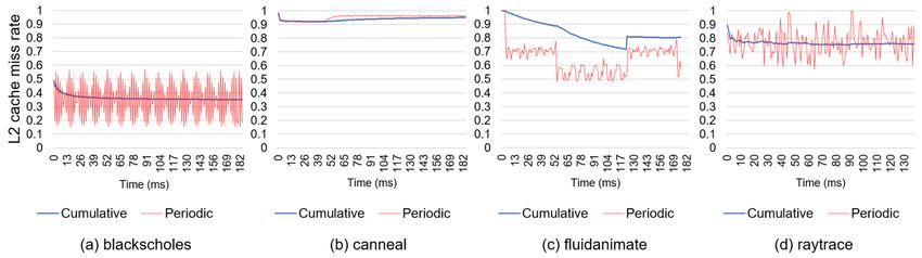
FIGURE 5. Profiled L2 cache miss rates of PARSEC applications (epoch T=1ms).
TABLE II
excessive eviction overhead. Our proposed unified L2
MEMORY PARTITIONING OF THE UNIFIED L2 TLB-CACHE TLB-cache controller prevents unnecessarily frequent
DEPENDING ON CONFIGURATIONS*. changes of the memory configuration by exploiting
counters for each configuration (as described in Figure 4).
Parameter Baseline Half-L2$ Bypass-L2$
In case of canneal (Figure 5(b)), the L2 cache miss rate is
L2 TLB (KB) 32KB (S) 128KB (M) 256KB (S+M) always much higher than thresholdhigh. In this case,
(2K entries) (8K entries) (16K entries) bypassing L2 cache would have little impact on
performance while providing much better energy efficiency.
L2 cache (KB) 256KB (S) 128KB (S) 0
Therefore, in case of canneal, our proposed controller sets
Write buffer (KB) 0 32KB (S) 32KB (S) Bypass-L2$ configuration to the unified L2 TLB-cache
(2K entries) (2K entries) memory. In case of fluidanimate shown in Figure 5(c), most
‘S’ and ‘M’ stand for SRAM and MRAM, respectively. of the profiled L2 cache miss rate values are in between
* Note the total capacity (L2 TLB + L2 cache + Write buffer) is same thresholdlow and thresholdhigh, which means that Half-
for all the configurations for fair comparison.
L2$ configuration would be better than other configurations.
SRAM/MRAM arrays for L2 TLB. In this case, all the L2
In case of raytrace (Figure 5(d)), though there are
cache accesses are bypassed to the shared L3 cache.
fluctuations in the profiled L2 cache miss rate, our
Furthermore, we adopt a 4-bit counter for each configuration,
proposed controller applies Half-L2$ to the unified L2
considering the fluctuations of the profiled L2 cache miss
TLB-cache memory according to the Half-L2$ counter hits
rate. Thus, only if one of the counters becomes all ones
all ones earlier than the Bypass-L2$ counter. According to
(meaning that the profiled L2 cache miss rate is expected to
our analysis, the L2 cache miss rate of an application does
last during runtime of the application), our proposed
not vary significantly during runtime. Thus, our proposed
controller ○
3 sets the target memory configuration depending
unified L2 TLB-cache controller offers an appropriate
on the profiled L2 cache miss rate; otherwise, it ○
4 maintains
memory configuration reflecting the application
all counters without changing the memory configuration until
characteristics, with negligible eviction overhead.
any counter becomes all ones. When the application is
terminated, the operating system can reset the proposed V. EVALUATION
controller and thus the memory configuration is restored to
the baseline. In our study, we set thresholdlow and A. Evaluation Methodology
thresholdhigh to 0.5 (50%) and 0.8 (80%), respectively. We analyze the impact of M3D-based SRAM/MRAM hybrid
Figure 5 shows cumulative and periodic L2 cache miss memory with our proposed unified L2 TLB-cache controller,
rates of four PARSEC benchmark applications profiled in terms of L2 TLB miss rate, performance, and energy
every 1ms. As shown in Figure 5(a), blackscholes has low consumption. For this purpose, we implement our proposed
cumulative L2 cache miss rate, which is lower than unified L2 TLB-cache controller by extending Sniper
thresholdlow. However, the profiled L2 cache miss rate of simulator [5]. To reflect the M3D-based SRAM/MRAM
blackscholes is intermittently higher than thresholdlow (0.5). hybrid memory, we apply the latency and energy parameters
If our proposed controller changes the memory described in Table I to the unified L2 TLB-cache memory.
configuration into Half-L2$, whenever the profiled L2 Table III shows the architectural parameters used in our
cache miss rate >thresholdlow, the performance of evaluation. The parameters of private resources are similar to
blackscholes could be degraded, since the profiled L2 cache a commercial microprocessor specification [28]. In our
miss rate becomes lower than thresholdlow in the next epoch simulation, each processor core has its own private L1/L2
time. In this case, frequent changes of the memory caches and TLBs, and all the cores share the L3 cache as the
configuration between the baseline and Half-L2$ causes last-level cache. ’Baseline’ and ’Proposed’ have only
VOLUME XX, 2021 7
This work is licensed under a Creative Commons Attribution 4.0 License. For more information, see https://creativecommons.org/licenses/by/4.0/This article has been accepted for publication in a future issue of this journal, but has not been fully edited. Content may change prior to final publication. Citation information: DOI
10.1109/ACCESS.2021.3054021, IEEE Access
TABLE III
ARCHITECTURAL SIMULATION PARAMETERS.
Parameter Baseline Proposed
Processor core 4-core, Octa-core, 22nm
ITLB (private) 128 entries, 4-way
DTLB (private) 64 entries, 4-way
L1 Icache 32KB, 8-way, 2 cycles
L1 Dcache 32KB, 8-way, 2 cycles
L2 TLB 2048 entries,
32KB: SRAM (Write buffer)
(private) 4-way, 2 cycles
256KB (Unified L2 TLB-cache):
L2 cache 256KB,
128KB SRAM + 128KB MRAM
(private) 8-way, 5 cycles
L3 cache FIGURE 6. L2 TLB miss rate of PARSEC applications depending on
8MB, 16-way, 30 cycles
(shared) configurations (Baseline Proposed).
Page walk
200 cycles
penalty the Bypass-L2$. Thus, by increasing the L2 TLB size, while
Benchmark blackscholes, canneal, dedup, facesim,
applications fluidanimate, raytrace, streamcluster
decreasing the L2 cache size, our proposed controller
eliminates most (99.7%) of the L2 TLB misses of
difference in L2 TLB and L2 cache specifications. To adopt a streamcluster as shown in Figure 6, compared to the baseline.
realistic value of page walk penalty, we measured the page Meanwhile, in case of fluidanimate and raytrace which have
walk latency in our experimental environment by using Intel the L2 cache miss rate between thresholdlow and thresholdhigh,
VTune Profiler [15]. Based on the real measurement, we our proposed controller applies Half-L2$ configuration to the
adopt 200 cycles for the page walk penalty. For benchmark unified L2 TLB-cache architecture, Thus, in case of
applications, we simulate the entire region of interest (ROI) fluidanimate and raytrace, our proposed controller reduces
of each PARSEC benchmark application described in Table the L2 TLB miss rate by 29.4% and 7.1%, compared to the
III, using simlarge input data set [4]. baseline respectively.
C. Performance
B. L2 TLB Miss Rate
Figure 6 depicts the L2 TLB miss rate of PARSEC Our proposed controller changes memory configurations of
applications. Among the applications, since blackscholes and the unified L2 TLB-cache architecture depending on the
facesim have low L2 cache miss rate (This article has been accepted for publication in a future issue of this journal, but has not been fully edited. Content may change prior to final publication. Citation information: DOI
10.1109/ACCESS.2021.3054021, IEEE Access
FIGURE 8. Normalized energy consumption (L2 TLB + L2 cache) of PARSEC applications depending on configurations.
performance. accesses due to TLB misses, we compare the memory energy
Figure 7 depicts the performance impact of our proposed consumption between baseline and our proposed technique.
controller with 2D and M3D-based SRAM/MRAM hybrid Figure 8 shows the energy consumption of L2 TLB and L2
memory, compared to the baseline with 2D and M3D-based cache, which is normalized to the energy consumption in the
SRAM-only memory. As shown in Figure 7, our proposed baseline with the 2D SRAM-only memory. As shown in
controller has a marginal impact on performance for most Figure 8, our proposed architecture with the M3D-based
cases, compared to the baseline with 2D SRAM-only SRAM/MRAM hybrid memory provides much lower energy
memory. In addition, since it is able to hide performance than the other configurations. In case of blackscholes and
impact of long MRAM write latency by utilizing SRAM facesim, our proposed controller with the M3D-based
write buffer, our proposed controller with M3D-based SRAM/MRAM hybrid memory reduces energy consumption
SRAM/MRAM hybrid memory does not incur performance by 19.9% and 42.9%, respectively, compared to the baseline
degradation compared to the baseline with M3D-based with the 2D SRAM-only memory. In addition, our proposed
SRAM-only memory. In case of canneal and streamcluster, controller with the M3D-based SRAM/MRAM hybrid
our proposed controller with M3D-based SRAM/MRAM memory shows 6.5% (blackscholes) and 11.2% (facesim)
hybrid memory improves the performance by 2.7% and 1.5%, lower energy than the baseline with the M3D-based SRAM-
respectively, compared to the baseline with 2D SRAM-only only memory. Though our proposed controller does not
memory. In case of dedup, our proposed controller with change the memory configuration due to low L2 cache miss
M3D-based SRAM/MRAM hybrid memory slightly rate (thresholdhigh). As a result, our proposed controller provides
51.8%, 97.7%, and 93.2% lower energy consumption in the
D. Energy Consumption unified L2 TLB-cache for canneal, dedup, and streamcluster,
With negligible impact on performance, our proposed respectively, compared to the baseline with 2D SRAM-only
architecture improves energy efficiency significantly, since memory. Especially, our proposed architecture is
we exploit the M3D-based SRAM/MRAM hybrid memory significantly beneficial for dedup and streamcluster,
for the unified L2 TLB-cache architecture. We compare the compared to the other applications. The reason is that our
energy consumption of L2 TLB+L2 cache for four different proposed architecture reduces the unnecessarily wasted
configurations: i) Baseline with the 2D SRAM-only memory, energy for L2 cache accesses in dedup and streamcluster,
ii) Baseline with the M3D-based SRAM-only memory, iii) while the applications (dedup and streamcluster) do not incur
Our proposed architecture with the 2D SRAM/MRAM a large number of L2 TLB accesses. Due to the reason, for
hybrid memory, and iv) Our proposed architecture with the dedup and streamcluster, our proposed controller with the
M3D-based SRAM/MRAM hybrid memory. Furthermore, as M3D-based SRAM/MRAM hybrid memory shows much
our proposed technique reduces the number of memory lower energy consumption in L2 TLB+L2 cache, even
VOLUME XX, 2021 9
This work is licensed under a Creative Commons Attribution 4.0 License. For more information, see https://creativecommons.org/licenses/by/4.0/This article has been accepted for publication in a future issue of this journal, but has not been fully edited. Content may change prior to final publication. Citation information: DOI
10.1109/ACCESS.2021.3054021, IEEE Access
FIGURE 9. Normalized memory access energy consumption depending on configurations (Baseline and Proposed).
compared to the baseline with the M3D-based SRAM-only with high L2 cache miss rate, where our proposed controller
memory. applies Bypass-L2$ configuration to the unified L2 TLB-
Lastly, in case of fluidanimate and raytrace, our proposed cache. Thus, such applications (e.g., canneal, dedup, and
controller applies the Half-L2$ configuration to the unified streamcluster) have energy reduction in the main memory as
L2 TLB-cache, reflecting the profiled L2 cache miss rate. As well as the unified L2 TLB-cache. On average, our proposed
shown in Figure 8, our proposed controller with 2D technique reduces the memory access energy consumption
SRAM/MRAM hybrid memory results in slightly higher by 10.9% for PARSEC benchmark applications.
energy consumption than the baseline, since 2D
SRAM/MRAM hybrid memory does not lead to wire energy VI. DISCUSSION
reduction, compared to the 2D SRAM-only memory.
Additionally, our proposed controller adds energy A. Potential Impacts of Monolithic 3D ICs
consumption by buffering write operations, so that our Thermal Problem: As many researchers have considered,
proposed controller with 2D SRAM/MRAM hybrid memory thermal problem is a major concern of 3D stacking of
does not provide energy reduction. On the other hand, when logic/memory architectures. Especially, in the case of TSV-
using M3D-based SRAM/MRAM hybrid memory, the 3D, the bonding layer is too thick (e.g., ~2.5um), so that it
energy consumption for SRAM arrays is reduced, thanks to impedes vertical heat flow towards heat sink, which in turn
the wire energy reduction. As a result, our proposed increases temperature of bottom layer seriously. However, in
controller with M3D-based SRAM/MRAM hybrid memory contrast to the TSV-3D, M3D has better thermal
reduces L2 TLB+L2 cache energy consumption by 36.9% characteristics due to the interlayer dielectric (ILD) which is
and 32.8% in case of fluidanimate and raytrace, respectively. much thinner than the bonding layer in the TSV-3D designs.
Meanwhile, in case of raytrace, our proposed controller with Thus, M3D has been considered to be more robust to thermal
the M3D-based SRAM/MRAM hybrid memory has slightly problem rather than TSV-3D. To examine the thermal impact
higher energy consumption, compared to the baseline with of our proposed architecture, we execute HotSpot thermal
the M3D-based SRAM-only memory. In this case, as our simulation reflecting the SRAM/MRAM hybrid memory; we
proposed controller adopts Half-L2$ configuration to the use the detailed layer material properties from [10].
unified L2 TLB-cache architecture, it causes slightly more According to our analysis, the CPU peak temperature reaches
L2 cache misses, which in turn increases the overall energy 83.2˚C in case of raytrace (i.e., the most compute-intensive
consumption due to the increased SRAM accesses. application), which is still lower than DTM trigger
Figure 9 shows the memory access energy consumption temperature (i.e., 90˚C) of modern microprocessors. Several
depending on configurations. Since our proposed technique previous studies on M3D [10][18] also report that M3D-
reduces the number of memory accesses due to TLB misses based microprocessors may not suffer from thermal problem
significantly, it leads to considerable memory access energy even with 4-layer stacking, since M3D leads to lower energy
reduction. As shown in Figure 9, in the best case (canneal), consumption as well as better heat conduction than TSV-3D.
our proposed technique reduces the memory access energy Consequently, our proposed M3D hybrid architecture does
consumption by 32.9%, as it reduces the memory access not incur thermal problem, while it reduces system-wide
energy due to TLB misses by 41.7%. In case of streamcluster, energy significantly.
our proposed technique reduces the memory access energy Noise Characteristics: Though the TSV-3D has been proved
consumption by 21.4% by eliminating most of the TLB not appropriate for 3D stacking of memory cells due to the
misses. Our proposed technique is beneficial for applications poor alignment precision and area overhead. Furthermore,
TSV-3D causes significant leakage power in TSVs and its
VOLUME XX, 2021 10
This work is licensed under a Creative Commons Attribution 4.0 License. For more information, see https://creativecommons.org/licenses/by/4.0/This article has been accepted for publication in a future issue of this journal, but has not been fully edited. Content may change prior to final publication. Citation information: DOI
10.1109/ACCESS.2021.3054021, IEEE Access
buffer chains, which affects noise margin. On the contrary, unified L2 TLB-cache architecture, it consumes much
M3D would have much better noise characteristics than smaller energy compared to the conventional 2D SRAM-
TSV-3D, due to the following reasons. First, the M3D has only memory. According to our analysis, our proposed
negligible leakage power in MIVs. Second, the ILD layers in controller with the M3D-based SRAM/MRAM hybrid
M3D act as noise shielding layer between two active layers. memory reduces the energy consumption of L2 TLB and L2
Thus, several previous works have shown that M3D-based cache by 53.6%, on average, compared to the 2D-SRAM
SRAM/NVMs have strong noise margin [18][24][31][34]. In only memory. Furthermore, our proposed technique leads to
addition, the coupling effect between layers can be controlled memory energy reduction by up to 32.9%, Consequently, our
in design time by adjusting ILD thickness with negligible proposed technique makes the unified L2 TLB-cache
performance impact; while increasing ILD thickness, the architecture more energy-efficient by using M3D technology.
thickness is much thinner (shorter) compared to the 2D wire We expect that our proposed technique will be adopted to
length. future M3D-based microprocessors to enhance energy
efficiency.
B. Monolithic 3D Fabrication of SRAM-MRAM Hybrid
Memories ACKNOWLEDGMENT
Though several studies have applied M3D integration to The present research has been conducted by the Research
SRAM-only architecture [10][21], M3D stacking of SRAM- Grant of Kwangwoon University in 2020. This work was
only memory banks may cause transistor performance also supported by the National Research Foundation of
degradation due to the low temperature process of M3D Korea (NRF) grant funded by the Korea government (MSIT)
fabrication. On the other hand, since MRAM is originally (No. NRF-2020R1G1A1100040)
fabricated at low temperature, it can be stacked without the
damage to the bottom (i.e., SRAM) layer, while not causing REFERENCES
transistor performance degradation. Due to the reason, non- [1] J. Ahn, S. Yoo and K. Choi, "Prediction Hybrid Cache: An Energy-
Efficient STT-RAM Cache Architecture," in IEEE Transactions on
volatile memories such as MRAM have been considered to Computers, vol. 65, no. 3, pp. 940-951, 1 March 2016.
be good candidates for memory/storage layers in M3D ICs [2] ARM. 2017.ARM Cortex-A75 Specifications. [Online]
[38][39][42]. https://developer.arm.com/ip-products/processors/cortex-a/cortex-
a75
Nevertheless, for the mass production of M3D ICs, it is [3] A. Bhattacharjee and M. Martonosi. "Inter-core cooperative TLB for
certain that M3D fabrication technology needs to be further chip multiprocessors." ACM Sigplan Notices, vol. 45, no. 3, pp. 359-
improved with cost reduction. Thus, many researchers have 370, 2010.
[4] C. Bienia, S. Kumar, J. P. Singh, and K. Li, “The PARSEC
tried to improve M3D fabrication technology in various benchmark suite: Characterization and architectural implications,”
levels of studies, such as layer/via materials, fabrication Proceedings of the 17th international conference on Parallel
methods, CAD tools, etc. [18][19][27]. architectures and compilation techniques, pp. 72-81, 2010.
[5] T. E. Carlson, H. Wim, and E. Lieven, "Sniper: Exploring the level
of abstraction for scalable and accurate parallel multi-core
VII. CONCLUSION simulation," Proceedings of 2011 International Conference for High
Emerging workloads have varying characteristics in private Performance Computing, Networking, Storage and Analysis. Pp. 72-
L2 TLB and L2 cache. Nevertheless, modern 81, 2011.
[6] J. H. Cho et al., "A 1.2V 64Gb 341GB/S HBM2 stacked DRAM
microprocessors still have private L2 TLB and L2 cache with
with spiral point-to-point TSV structure and improved bank group
fixed capacities, which causes inefficiency in performance data control," 2018 IEEE International Solid-State Circuits
and energy consumption. Especially, emerging parallel Conference (ISSCC), pp. 208-210, 2018.
workloads have high miss rate in private L2 cache due to [7] X. Dong, C. Xu, Y. Xie and N. P. Jouppi, "NVSim: A Circuit-Level
Performance, Energy, and Area Model for Emerging Nonvolatile
large working set size, and they also suffer from high L2 Memory," in IEEE Transactions on Computer-Aided Design of
TLB miss rate, resulting in significant main memory accesses Integrated Circuits and Systems, vol. 31, no. 7, pp. 994-1007, July
for page table walks. 2012.
[8] M. S. Ebrahimi et al., “Monolithic 3D integration advances and
In this paper, we propose an energy-efficient unified L2 challenges: From technology to system levels,” 2014 SOI-3D-
TLB-cache architecture exploiting M3D-based Subthreshold Microelectronics Technology Unified Conference (S3S).
SRAM/MRAM hybrid memory. We consider the unified L2 IEEE, 2014.
[9] W. Gomes et al., "8.1 Lakefield and Mobility Compute: A 3D
TLB-cache architecture, while the conventional architecture Stacked 10nm and 22FFL Hybrid Processor System in 12×12mm2,
uses the L2 TLB and L2 cache separately. Our proposed 1mm Package-on-Package," IEEE International Solid- State Circuits
controller applies different memory configurations (i.e., Conference - (ISSCC), pp. 144-146, 2020.
Baseline, Half-L2$, and Bypass-L2$) depending on the L2 [10] Y. Gong, J. Kong and S. W. Chung, "Quantifying the Impact of
Monolithic 3D (M3D) Integration on L1 Caches," in IEEE
cache miss rate. By reconfiguring the unified L2 TLB-cache Transactions on Emerging Topics in Computing, published online.
architecture, our proposed controller reduces the L2 TLB [11] K. Gopalakrishnan, et al., “Highly-scalable novel access device
miss rate 7.14%~99.73%, with negligible performance based on Mixed Ionic Electronic conduction (MIEC) materials for
high density phase change memory (PCM) arrays,” 2010 Symposium
overhead. Furthermore, as our proposed technique utilizes on VLSI Technology. IEEE, 2010.
the M3D-based SRAM/MRAM hybrid memory for the
VOLUME XX, 2021 11
This work is licensed under a Creative Commons Attribution 4.0 License. For more information, see https://creativecommons.org/licenses/by/4.0/This article has been accepted for publication in a future issue of this journal, but has not been fully edited. Content may change prior to final publication. Citation information: DOI
10.1109/ACCESS.2021.3054021, IEEE Access
[12] B. Gopireddy and J. Torrellas, "Designing Vertical Processors in [31] C.-H. Shen, et al., “Monolithic 3D Chip Integrated with 500ns NVM,
Monolithic 3D," 2019 ACM/IEEE 46th Annual International 3ps Logic Circuits and SRAM,” IEEE International Electron Devices
Symposium on Computer Architecture (ISCA), pp. 643-656, 2019. Meeting, 2013
[13] A. Hankin, T. Shapira, K. Sangaiah, M. Lui, and M. Hempstead. [32] J. Shi, D. Nayak, M. Ichihashi, S. Banna and C. A. Moritz, "On the
“Evaluation of Non-Volatile Memory Based Last Level Cache Given Design of Ultra-High Density 14nm Finfet Based Transistor-Level
Modern Use Case Behavior.” IEEE International Symposium on Monolithic 3D ICs," 2016 IEEE Computer Society Annual
Workload Characterization (IISWC), November 3-5, 2019. Symposium on VLSI (ISVLSI), pp. 449-454, 2016.
[14] D. B. Ingerly et al., "Foveros: 3D Integration and the use of Face-to- [33] M. M. Shulaker et al., "Monolithic 3D integration of logic and
Face Chip Stacking for Logic Devices," IEEE International Electron memory: Carbon nanotube FETs, resistive RAM, and silicon FETs."
Devices Meeting (IEDM), pp. 19.6.1-19.6.4, 2019 2014 IEEE International Electron Devices Meeting. IEEE, 2014.
[15] Intel VTune Profiler. https://software.intel.com/content/www/us/en/ [34] S. Srinivasa, et al. "ROBIN: Monolithic-3D SRAM for enhanced
develop/tools/vtune-profiler.html robustness with in-memory computation support." IEEE
[16] G. Jan et al., “Demonstration of fully functional 8mb perpendicular Transactions on Circuits and Systems I: Regular Papers, vol. 66, no.
stt-mram chips with sub-5ns writing for non-volatile embedded 7, pp. 2533-2545, 2019.
memories,” 2014 Symposium on VLSI Technology (VLSI [35] G. Sun, X. Dong, Y. Xie, J. Li and Y. Chen, "A novel architecture of
Technology): Digest of Technical Papers, June 2014, pp. 1–2. the 3D stacked MRAM L2 cache for CMPs," IEEE 15th
[17] W. Jeon, J. H. Park, Y. Kim, G. Koo and W. W. Ro, "Hi-End: International Symposium on High Performance Computer
Hierarchical, Endurance-Aware STT-MRAM-Based Register File for Architecture, pp. 239-249, 2009
Energy-Efficient GPUs," in IEEE Access, vol. 8, pp. 127768-127780, [36] H. Sun, C. Liu, W. Xu, J. Zhao, N. Zheng and T. Zhang, "Using
2020. Magnetic RAM to Build Low-Power and Soft Error-Resilient L1
[18] J. Jiang, K. Parto, W. Cao, and K. Banerjee, “Ultimate Monolithic- Cache," in IEEE Transactions on Very Large Scale Integration
3D Integration With 2D Materials: Rationale, Prospects, and (VLSI) Systems, vol. 20, no. 1, pp. 19-28, Jan. 2012.
Challenges,” IEEE Journal of the Electron Devices Society, vol.7, pp. [37] G. Venkatasubramanian, R. J. Figueiredo, R. Illikkal and D. Newell,
878-887, 2019. "A Simulation Framework for the Analysis of the TLB Behavior in
[19] P. S. Kanhaiya, et al., “X3D Heterogeneous Monolithic 3D Virtualized Environments," IEEE International Symposium on
Integration of X (Arbitrary) Nanowires Silicon, III–V, and Carbon Modeling, Analysis and Simulation of Computer and
Nanotubes,” IEEE Transactions on Nanotechnology, vol. 18, pp. Telecommunication Systems, pp. 211-221, 2010.
270-273, 2019. [38] H. Wong and S. Salahuddin, “Memory leads the way to better
[20] J. Kong, "A novel technique for technology-scalable STT-RAM computing,” Nature Nanotech vol. 10, no. 3 pp. 191–194, 2015.
based L1 instruction cache." IEICE Electronics Express (2016). [39] Y. Yu and N. K. Jha, “SPRING: A Sparsity-Aware Reduced-
[21] J. Kong, Y. Gong and S. W. Chung, "Architecting large-scale SRAM Precision Monolithic 3D CNN Accelerator Architecture for Training
arrays with monolithic 3D integration," IEEE/ACM International and Inference,” IEEE Transactions on Emerging Topics in
Symposium on Low Power Electronics and Design (ISLPED), Taipei, Computing, published online.
pp. 1-6, 2017. [40] Y. Zhang, Y. Li, Z. Sun, H. Li, Y. Chen and A. K. Jones, "Read
[22] D. U. Lee et al., "25.2 A 1.2V 8Gb 8-channel 128GB/s high- Performance: The Newest Barrier in Scaled STT-RAM," in IEEE
bandwidth memory (HBM) stacked DRAM with effective Transactions on Very Large Scale Integration (VLSI) Systems, vol.
microbump I/O test methods using 29nm process and TSV," IEEE 23, no. 6, pp. 1170-1174, June 2015.
International Solid-State Circuits Conference Digest of Technical [41] L. Zhu et al., "Heterogeneous 3D Integration for a RISC-V System
Papers (ISSCC), pp. 432-433, 2014. With STT-MRAM," in IEEE Computer Architecture Letters, vol. 19,
[23] S. Lee, K. Kang and C. Kyung, "Runtime Thermal Management for no. 1, pp. 51-54, May 2020.
3-D Chip-Multiprocessors With Hybrid SRAM/MRAM L2 Cache," [42] F. Zokaee, M. Zhang, X. Ye, D. Fan and L. Jiang, "Magma: A
in IEEE Transactions on Very Large Scale Integration (VLSI) Monolithic 3D Vertical Heterogeneous Reram-Based Main Memory
Systems, vol. 23, no. 3, pp. 520-533, March 2015. Architecture," 2019 56th ACM/IEEE Design Automation Conference
[24] C. Liu and S. K. Lim. “Ultra-high density 3D SRAM cell designs for (DAC), Las Vegas, NV, USA, pp. 1-6, 2019.
monolithic 3D integration,” IEEE International Interconnect
Technology Conference, 2012.
[25] X. Liu, Y. Li, Y. Zhang, A. K. Jones and Y. Chen, "STD-TLB: A
STT-RAM-based dynamically-configurable translation lookaside
buffer for GPU architectures," 2014 19th Asia and South Pacific
Design Automation Conference (ASP-DAC), Singapore, pp. 355-360,
2014.
[26] Y. Marathe, N. Gulur, J. H. Ryoo, S. Song, and L. K. John, “CSALT:
context switch aware large TLB,” Proceedings of the 50th Annual
IEEE/ACM International Symposium on Microarchitecture (MICRO-
50). Association for Computing Machinery, New York, NY, USA,
pp. 449–462, 2017.
[27] Z. Or-Bach, B. Cronquist, Z. Wurman, I. Beinglass, and A. K.
Henning, “Modified ELTRAN®—A game changer for Monolithic
3D,” IEEE SOI-3D-Subthreshold Microelectronics Technology YOUNG-HO GONG received the BS degree in the
Unified Conference (S3S), 2015. Division of Computer and Communication
[28] E. Rotem, "Intel architecture, code name Skylake deep dive: A new Engineering from Korea University, in 2012. He
architecture to manage power performance and energy efficiency," received the PhD degree in the Department of
Intel Developer Forum. Vol. 24. 2015. Computer Science and Engineering, Korea
[29] J. H. Ryoo, N. Gulur, S. Song, and L. K. John. "Rethinking TLB University, in 2018. He was a staff engineer in
designs in virtualized environments: A very large part-of-memory Samsung Electronics DS. He is currently an
TLB," ACM SIGARCH Computer Architecture News, vol. 45, no. 2, assistant professor in the School of Computer and
pp. 469-480, 2017. Information Engineering at Kwangwoon University.
[30] H. Sato, et al., “14ns write speed 128Mb density Embedded STT- His research interests include 3D-stacked system design, low-
MRAM with endurance>1010 and 10yrs retention@85°C using power/thermal-aware computer architecture design, and architecture-level
novel low damage MTJ integration process,” 2018 IEEE thermal modeling.
International Electron Devices Meeting (IEDM). IEEE, 2018.
VOLUME XX, 2021 12
This work is licensed under a Creative Commons Attribution 4.0 License. For more information, see https://creativecommons.org/licenses/by/4.0/You can also read