NANOESCA: A NOVEL ENERGY FILTER FOR IMAGING X-RAY PHOTOEMISSION SPECTROSOCPY - FOCUS GMBH
←
→
Page content transcription
If your browser does not render page correctly, please read the page content below
INSTITUTE OF PHYSICS PUBLISHING                                         JOURNAL OF PHYSICS: CONDENSED MATTER
J. Phys.: Condens. Matter 17 (2005) S1329–S1338                                 doi:10.1088/0953-8984/17/16/004

NanoESCA: a novel energy filter for imaging
x-ray photoemission spectrosocpy

                 M Escher1 , N Weber1 , M Merkel1 , C Ziethen2 , P Bernhard2 ,
                 G Schönhense2 , S Schmidt3 , F Forster3 , F Reinert3 , B Krömker4 and
                 D Funnemann4
                 1   Focus GmbH, 65510 Hünstetten, Germany
                 2   Johannes Gutenberg Universität Mainz, Institut für Physik, 55099 Mainz, Germany
                 3   Universität des Saarlandes, FR 7.2. Experimentalphysik, 66041 Saarbrücken, Germany
                 4   Omicron NanoTechnology GmbH, 65232 Taunusstein, Germany

                 E-mail: m.escher@focus-gmbh.com

                 Received 13 May 2004, in final form 9 December 2004
                 Published 8 April 2005
                 Online at stacks.iop.org/JPhysCM/17/S1329

                 Abstract
                 A novel instrument for imaging ESCA is described. It is based on a tandem
                 arrangement of two hemispherical energy analysers used as an imaging energy
                 filter. The main spherical aberration (α 2 -term) of the analyser is corrected
                 by the antisymmetry of the tandem configuration. The kinetic energy range
                 useable for imaging extends up to 1.6 keV; this is compatible with Mg and
                 Al Kα laboratory x-ray sources. First experiments on the chemical surface
                 composition of a Cu0.98 Bi0.02 polycrystal, a GaAs/AlGaAs heterostructure and
                 Ag crystallites on Si(111) have been performed using synchrotron radiation.
                 The results reveal an energy resolution of 190 meV and a lateral resolution
                 (edge resolution) of 120 nm. Besides elimination of the analyser’s spherical
                 aberration, the tandem arrangement largely retains the time structure of the
                 electron signal, unlike a single hemispherical analyser.

                 (Some figures in this article are in colour only in the electronic version)

1. Introduction

The worldwide advances in nanoscience and nanotechnology have strongly pushed the
development and improvement of adequate analytical methods. In the field of microscopy
there has been dramatic progress in imaging performance. Today scanning tunnelling
microscopy (STM) is a standard tool for imaging of conducting surfaces with atomic
resolution. Modern transmission electron microscopy (TEM) also provides atomic resolution,
0953-8984/05/161329+10$30.00       © 2005 IOP Publishing Ltd     Printed in the UK                          S1329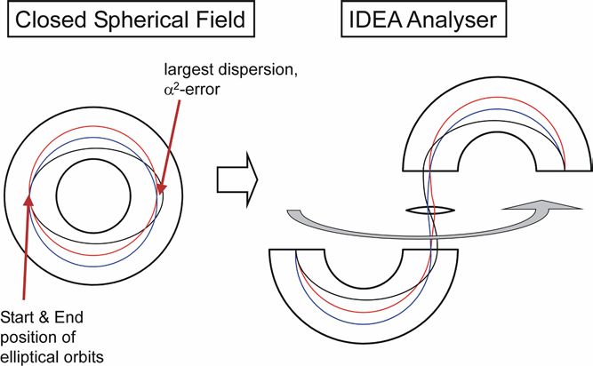
S1330                                                                                M Escher et al

and aberration correction [1] paves the way to ‘sub-Å resolution’ in the future [2]. Less
progress has been achieved in the field of nanospectroscopy. X-ray fluorescence (EDX) or
Auger microprobes in scanning electron microscopy reached their principal limits several years
ago. Their lateral and depth resolution is limited by electron scattering processes (blooming)
within the surface region of the sample. Further restrictions are the low x-ray fluorescence
yield and the low signal-to-background ratio of electron-excited Auger spectroscopy.
     The spectroscopic mode of STM works very well within a few electronvolts from the
Fermi edge [3], but gives no access to core levels, being the ‘fingerprint’ of elements and their
chemical environment in a compound. Energy-filtered TEM does give access to core levels via
electron energy loss spectroscopy (EELS) yielding the electron loss near-edge structure. The
performance of this technique is very high for specimens with good crystalline order being
sufficiently thin to transmit the electron beam. 3D nanodevices can only be studied when
thin samples are cut out exactly at the position of interest. For a fast control during a wafer
production, chemical surface reactions on a catalyst, etc, spectroscopic TEM is not suitable.
Obviously, there is still a strong need for other powerful tools for non-destructive chemical
nanoanalysis of surfaces of thick specimens.
     Looking at the problem with the eyes of a spectroscopist, we find x-ray induced
photoelectron spectroscopy the most powerful technique, named electron spectroscopy for
chemical analysis (ESCA). Established in the 1960s by Siegbahn et al [4], ESCA comprises x-
ray photoemission spectroscopy (XPS) and x-ray excited Auger electron spectroscopy (AES).
Characteristic x-ray lines (often Mg Kα at 1253.6 eV or Al Kα at 1486.6 eV) from water-
cooled anodes (fixed or rotating) or monochromatized synchrotron radiation are used to excite
photoelectrons and Auger electrons. Energy analysis of the electrons yields the core level
binding energies. This facilitates a fingerprint-like detection of elements and their chemical
states in compounds. Corresponding spectra of all elements (except H, He and the heavier
transuranium elements) and many compounds have been tabulated (e.g. [5]). This makes the
interpretation of spectra easy and reliable and allows for a quantitative analysis with reasonable
accuracy down to 4–5 at.% [6]. It is near at hand that the combination of ESCA with microscopy
provides an attractive surface analytical tool.
     There have been several approaches to combine ESCA with lateral resolution. A
straightforward way is to focus the x-ray beam in a small spot and scan the surface, taking
spectra at each point. This concept is used in various laboratories (e.g. [7]) and in a commercial
instrument [8]. The alternative way is parallel image acquisition via a magnifying lens system
and an imaging energy analyser. This approach provides both a higher data acquisition rate
and the possibility to take energy-filtered images at selected XPS lines and in real time.
     Early commercial solutions [9–11] added an imaging lens to a hemispherical energy
analyser; later designs [12–14] started from proven electron microscopes that were
complemented by energy analysers with good imaging capabilities. A fully aberration
corrected instrument is under construction and test [15].
     In order to fully exploit the potential of ESCA in an electron microscope, the energy range
accessible with Mg or Al Kα radiation should not be restricted. This poses a high challenge
to the electron optical design because Liouville’s theorem prevents feeding a large-solid-angle
ensemble of electrons starting at 1.5 keV kinetic energy into an energy analyser operating
at a pass energy of typically 100 eV or even less. In the present paper we describe a novel
solution that attacks the problem of phase-space volume by aberration correction (α 2 -term)
of the analyser. This is accomplished by the antisymmetry of a tandem configuration of two
hemispherical analysers. Besides elimination of the analyser’s spherical aberration the tandem
set-up largely retains the time structure of the electron signal, unlike a single hemisphere. This
is an important feature for future energy- and time-resolved studies.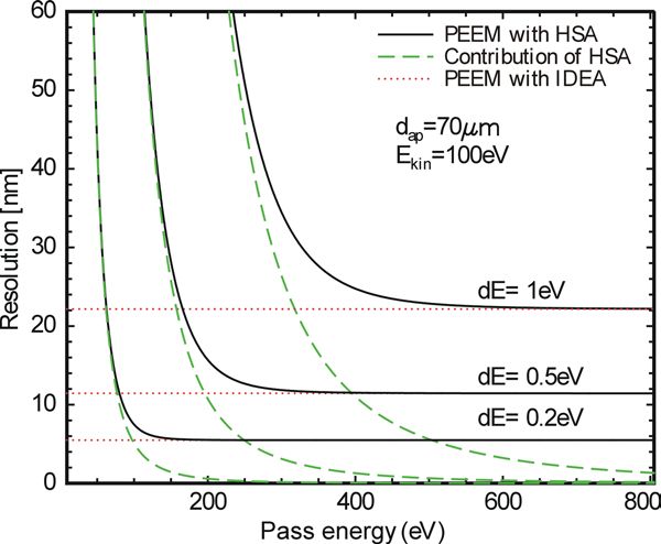
NanoESCA: a novel energy filter for imaging XPS                                                          S1331

                 Figure 1. Schematic layout of the nanoESCA instrument. The three paths of the electrons are
                 indicated: (1) PEEM-mode, (2) selected area spectroscopy, (3) energy-filtered ESCA imaging. The
                 grey box envelops the elements of the PEEM mode.

2. Description of the instrument
2.1. Basic concept
The instrument developed—called NanoESCA—is derived from an electrostatic photoemis-
sion electron microscope (PEEM) column and a twin hemispherical energy analyser (HSA).
Figure 1 shows a schematic view of the electron optical layout. The path of the electrons
for the three modes of operation are indicated: (1) direct non-energy-filtered PEEM imaging,
(2) selected area spectroscopy and (3) energy-filtered ESCA imaging for kinetic energies up
to 1.6 keV.
     The PEEM column is used as the entrance lens of the analyser. It consists of an immersion
objective lens with exchangeable and adjustable contrast apertures, an electrostatic octopole
stigmator and two projective lenses. A continuously adjustable iris aperture in the first
intermediate image plane is used to select a defined field of view for selected area spectroscopy.
The field of view can be chosen and defined in size and position using the direct PEEM imaging
mode. The projective lenses are either used to project the first intermediate image onto the
screen for direct non-energy-filtered imaging or to adapt the electron beam to the pass energy
of the analyser.
     The analyser of the nanoESCA (called the imaging double energy analyser, IDEA) is a
new development [16] essentially consisting of two hemispherical analysers. The action of
the two hemispheres is illustrated in figure 2. In the spherical electrostatic field, similarly to
planetary motion (Kepler ellipses), the trajectories of the electrons coincide after a complete
revolution, independent of the start energy and start angle, i.e. a perfect achromatic image
without aberrations is generated. The second half of the elliptical orbit compensates the
S1332 M Escher et al
Figure 2. Schematic illustration of the basic design idea for the imaging double energy analyser.
The different schematic particle trajectories are drawn for the same kinetic start energies.
aberrations of the first half. After 180◦ revolution the largest dispersion occurs. Here the
energy selecting slit is placed. The problem of this—so far theoretical—model is the transport
of electrons into and out of the inner and outer spheres, as they block the space for the entrance
lens and the detector. To solve this task we divided the spherical field into two halves, mirrored
the second and removed it from the first. A transfer lens images the electrons leaving the first
hemisphere onto the entrance of the second hemisphere.
For selected area spectroscopy the deflection field of the second hemisphere is switched
off. The electrons then are focused by the transfer lens into a channeltron detector. With
this detector quantitative spectra suitable for ESCA analysis can be obtained, without the
uncertainty of image conversion by the channelplate–screen–camera assembly.
The good lateral resolution of the microscope is accomplished by the immersion objective
lens, which consists of a sample near ground potential and an extractor anode that is kept at
up to 16 kV. The electrons decelerate towards the column, in contrast to other cathode lenses
where the drift energy of the electrons in the column equals the extractor energy [17]. We
found that the combined error due to spherical and chromatic aberrations can also be minimized
for a column potential of about 8% of the extracting voltage. This has the advantage that for
spectroscopic imaging a large part of the deceleration towards the analyser’s pass energy is
already done by the objective lens while maintaining the advantage of a high accelerating field
with small aberrations. The theoretical resolution limit of our cathode lens is about 10 nm
for non-energy-filtered threshold emission. We will show below that a low pass energy is an
advantage for the imaging with good spatial and energy resolution and with high transmission.
A typical pass energy for the nanoESCA instrument is 100 eV or below. For this pass energy
a deceleration of about one order of magnitude via the projective lenses is sufficient, and this
can be easily accomplished over a large range of magnifications.
2.2. Imaging mode: IDEA compared with HSA
The energy resolution of the IDEA analyser is defined by the slit at the exit of the first
hemisphere and therefore is identical to the energy resolution of a single HSA with the same
radius. The energy resolution E at a pass energy E pass of an HSA with mean path radius R
can be written as
d
E = E pass +α ,2
(1)
2RNanoESCA: a novel energy filter for imaging XPS S1333
Figure 3. Calculated pass energy dependence of the lateral resolution of an energy-filtered image,
comparing the nanoESCA with the HSA resolution at different energy resolutions dE. The starting
energy is E kin = 100 eV. The HSA contribution results from the α 2 -term in equation (1).
where d is the slit width and α is the maximum angle of electrons with respect to the optical
axis. The α 2 -term can be regarded as the spherical aberration of the analyser’s dispersion. A
good energy resolution E requires either a small pass energy E pass or a small slit width d,
providing the α 2-term is small enough. Which of the two terms should be minimized preferably
can be decided by discussing the transmission of the system. Neglecting all higher order terms,
the accepted phase space in dispersive direction at the entrance slit (or the linear transmission
of the HSA) can be written with help of equation (1):
E
Td ∝ E pass αd = α2R. (2)
E pass
Assuming a constant aperture angle α at the analyser’s entrance slit (in our configuration
depending only on the contrast aperture size or the field of view), it can be seen that at a
given energy resolution the transmission drops with increasing pass energies. This holds
for configurations with a reciprocal image plane in the analyser’s entrance as described by
Tonner [12] and Coxon [9, 10] that have a coupling lens between the image plane in front
of and behind the hemisphere and the entrance and exit slits. This lens maps an angular
distribution in the image plane into real space coordinates at the entrance or exit plane of the
analyser and vice versa. Calculating the transmission in the image plane, the coordinates can
be transformed into the entrance plane of the analyser, and the focal lengths cancel out in the
calculation.
We have calculated the contribution of an HSA analyser operated with coupling lenses to
the image aberrations as a function of the pass energy and compared it to the IDEA that can
be operated without or with coupling lenses. Assuming a spherical aberration of the coupling
lenses, the analyser’s transfer equation (1) gives rise to image aberrations through the α 2 -term.
An example for a typical setting with a large contrast aperture (70 µm diameter) and
a kinetic energy of 100 eV is shown in figure 3. Here the spherical aberration coefficient
of the HSA’s coupling lenses is Cs = 250 mm. The dotted curve shows that within this
calculation the spatial resolution of the IDEA is independent of the pass energy. In terms of
the chromatic aberrations the spatial resolution of the PEEM–IDEA combination is limited byS1334 M Escher et al
Figure 4. Spectroscopic investigations of a Cu0.98 Bi0.02 polycrystal. The measurements were
made with 50 eV pass energy and slits of 1 mm width. Left: imaging at the Bi 4f7/2 core-level on
the grains (open dots) and on the grain boundaries (filled dots), visible bright in the Bi image. Right:
Fermi edge of the same sample (dots). The analysis of the data leads to an analyser resolution of
E fwhm = 189 meV (see the text).
the chromatic aberration of the PEEM lens. For a single hemispherical analyser with entrance
and exit coupling lenses, the α 2 aberration blurs the image at low pass energies. Obviously
this aberration is compensated in the IDEA configuration by the second hemisphere. For
pass energies larger than 500 eV the effect becomes negligible. For high transmission a low
pass energy is favourable, as we saw above. The correction of the spherical aberration of the
dispersion achieved with IDEA analyser allows us to work in that region with good spatial
resolution.
3. Results
3.1. Spectroscopic performance
As an example of the good spectroscopic performance we show measurements made on a
Cu0.98 Bi0.02 polycrystal [18]. The Bi4f7/2 core level and the Fermi edge (figure 4) are detected
using a photon energy of hν = 600 and 605 eV at the UE-52/SGM undulator micro-spot
beamline [19] at BESSYII. The photon flux was 3 × 10¹² photons mm−2 s−1 into a spot of
about 300 µm FWHM as was measured with the nanoESCA. The pass energy of the analyser
was 50 eV; the slit width at entrance and exit was 1 mm. The acquisition time for one image
was 60 s, and it was 20 s for the Fermi-edge measurements. In an image series taken at
binding energies around the Bi 4f7/2 XPS line (the upper left of figure 4 shows the image takenNanoESCA: a novel energy filter for imaging XPS S1335
Figure 5. Left: GaAs/Al(0.65)Ga(0.35)As heterostructure imaged at the Al 2p core level
(hν = 120 eV, pass energy 100 eV). Right: intensity profile over the area indicated on the left.
at E B = 156.83 eV) only the grain boundaries appear bright. The measurement shows the
segregated Bi located in the grain boundaries of the Cu grains of the crystal whereas only very
small Bi concentration is detected on the Cu grains themselves. This low background intensity
demonstrates the capability of the instrument for spectroscopic imaging.
The measurement revealed that Bi segregates to the boundaries between the Cu grains
of the crystal; no Bi concentration was detected on the Cu grains. This low background
intensity demonstrates the capability of the instrument for spectroscopic imaging. In the
image taken at the Bi 4f7/2 XPS line (upper left), only the grain boundaries appear bright. The
energy resolution of the measurements was determined by measuring the Fermi edge at room
temperature. The measured energy width of E exp = 230 meV (12%–88% rise) consists
of three intrinsic widths: the thermal width of the Fermi edge at room temperature (about
4kB T ≈ 102 meV), the photon bandwidth of the synchrotron beamline (Ph = 80 meV, [20]),
and the analyser’s energy resolution E. For simplicity, we fit the measured Fermi edge
by an effective Fermi–Dirac distribution plus linear background. One of the fit parameters
is a pseudo-temperature Tm which gives the experimental width E exp = 4kB Tm of the
Fermi edge including thermal and instrumental broadenings. From this experimental width,
the energy
resolution can be extracted in a simple and sufficiently accurate way to be
E = (4kB Tm )2 − Ph 2
− (4kB T )2 = 190 meV [21]. This measured energy resolution
is even better than the value calculated using equation (1), as the PEEM lens forms a virtual
slit at the analyser’s entrance which is smaller than 1 mm.
3.2. Spatial resolution with synchrotron excitation
As a test structure for the spatial resolution imaging electrons of an XPS line we used
a GaAs/Al0.65 Ga0.35 As heterostructure [22]. The sample consists of alternating layers of
different thicknesses that are cut and polished perpendicular to the layers. Before the
measurement the sample was cleaned by Ar-ion sputtering. With an excitation energy of
hν = 120 eV and about 1012 photons mm−2 s−1 we imaged the Al 2p core level at a kinetic
energy of 44 eV. The pass energy of the analyser was 100 eV for these measurements. Figure 5
shows an image of the sample and an intensity scan across the area indicated. The acquisition
time was 300 s.
The 500 nm wide line at the left-hand side gives a very high contrast of about 88% of the
Al 2p-intensity with respect to the background intensity taken far away from the Al features.S1336 M Escher et al
Figure 6. Ag crystallites on Si(111) imaged with direct PEEM mode (left) and energy-filtered
imaging (right). The energy-filtered image shows no deterioration due to the energy filtering but
a higher contrast. The PEEM image is assembled of two images with different contrast aperture
positions. The image acquisition time was 6 s in both the energy-filtered and unfiltered modes.
Alternating 300 nm wide lines separated by 300 nm spaces, which appear at the right-hand
side of the image, are resolved with a contrast of 58 ± 3% and an edge resolution of 120 nm
(intensity rise from 16% to 84%). Isolated 50 nm wide lines are clearly distinguishable from the
background intensity. The data have been taken with no vibrational damping of the instrument
and therefore mechanical vibrations in the synchrotron environment are supposed to be the
limiting factor for lateral resolution at the current state of development.
3.3. Comparison of energy-filtered and non-energy-filtered imaging
We compared the PEEM mode and the energy-filtered imaging mode using an Hg high-pressure
UV lamp working in the threshold excitation regime. The sample was Ag crystallites on an
Si(111) surface. Ag was deposited by e-beam evaporation on a clean Si(111) surface kept at
elevated temperature (T about 500 K) ex situ. At the given conditions the Ag dots showed a
width of typically some 100 nm to some microns. The size of the dots was calibrated using
scanning electron microscopy (SEM) prior to the PEEM measurements.
Figure 6 shows a comparison of images taken in the two modes (1 and 3 in figure 1) with
a comparable field of view. The Ag dots appear bright on the darker Si substrate. The Si
substrate has no uniform intensity as seen with the SEM; a wide wavy line running from top to
bottom of the images and some smaller lines running diagonally from the lower left side across
the sample can be assigned to terrace edges corresponding to multi-atomic steps. The terrace
edges appear bright or dark depending on position of the contrast aperture used. This is seen in
the PEEM image that is combined from two images with different contrast aperture positions.
Additionally the terrace edges are not imaged as sharply as the Ag dots. The local field at the
edges is probably distorted by two effects: the topography of the edge and a different work
function of the Si surface differing from the (111)-orientation. Consequently, the electron
trajectories are bent and appear under a changed emission angle [23].NanoESCA: a novel energy filter for imaging XPS S1337
The energy-filtered image (figure 6, right) was taken at an analyser pass energy of 100 eV.
The kinetic energy was set to give highest intensity in the Ag dots. The image has the same
quality with respect to lateral resolution and distortion-free imaging as the unfiltered PEEM
image. In the energy filtered mode the resolution for this sample was 80 nm. The contrast of
the Ag dots to the background is enhanced by the energy filtering. This can be explained by
a lower work function of the Ag dots. Optimizing the intensity of the Ag structure, a kinetic
energy was chosen close to the spectrometer cut-off at the maximum of the photoelectron
distribution. Assuming a higher work function of the Si substrate, the Si appears darker as its
emission lies within the spectrometer cut-off region due to the different work function. In our
case it is not possible to assign definite work function differences to the surfaces imaged as they
were not atomically clean due to the ex situ preparation. In general it is easily possible to study
quantitatively work function differences and image structure using this contrast mechanism
even with threshold emission.
4. Conclusions
A novel approach for imaging ESCA with lateral resolution in the 100 nm range was described.
In order to be compatible with the widely used Mg and Al Kα laboratory x-ray sources
delivering photon energies of 1253.6 and 1486.6 eV, respectively, the useable kinetic energy
range extends up to 1.6 keV. At such high kinetic energies, the conservation of phase-space
volume (Liouville’s theorem) is a serious electron optical problem. Retardation of an electron
beamlet starting at 1.5 keV kinetic energy to a typical analyser pass energy of 100 eV results in
an enhancement of the angular divergence by almost a factor of 4 (at constant magnification).
This, in turn, deteriorates the energy resolution and imaging quality of a hemispherical analyser.
Thus, the angular divergence needs to be restricted by an aperture stop in the reciprocal image
plane, leading to a strong reduction of intensity. In the present tandem configuration this α 2 -
term of the spherical aberration of the analyser is eliminated due to the antisymmetry of the
tandem configuration of two identical analysers.
The entrance lens is based on an electrostatic photoemission electron microscope column
with integrated sample stage. A standard sample holder (OMICRON type) facilitates easy and
fast sample exchange. Non-energy-filtered PEEM imaging is easily accomplished by switching
off the analyser potentials (‘straight-through-mode’). Another mode of operation is selected-
area microspectroscopy, facilitated by switching off the second hemispherical analyser and
using a channeltron electron detector behind the exit of the first analyser.
First test operation of the instrument employed synchrotron radiation at the UE-52/SGM
Undulator beamline at BESSY II. An analyser resolution of 190 meV has been determined at
a photon energy of 605 eV.5 The spatial resolution has been measured using a semiconductor
heterostructure yielding an edge resolution of 120 nm. Both values will certainly be improved
in the future by more optimized settings of the electron optics and by eliminating mechanical
vibrations. The imaging quality of the analyser has been tested in threshold photoemission
using a Hg high-pressure UV lamp. Ag crystallites on Si(111) grown by e-beam deposition
at elevated temperature showed a higher contrast and no reduction in lateral resolution in the
energy-filtered images as compared to the non-filtered image of the same sample position.
This result ensured that no visible image deterioration and no distortion occurred upon energy
filtering.
Besides its capability of energy-resolved imaging on a selected XPS-line (imaging ESCA),
the instrument strongly improves the resolution in synchrotron-radiation-based X-PEEM. This
5 Recently, an energy resolution of 110 meV (12%–88% rise) has been reached at 80 keV kinetic energy in the soft
x-ray range.S1338 M Escher et al
is a consequence of a strong reduction of the chromatic aberration of the imaging optics
(essentially the electrostatic extractor field) by selecting a narrow energy interval of electrons
forming the image. Usually, very small aperture stops in the back focal plane of the objective
lens have to be used to minimize the chromatic aberration. However, this dramatically reduces
the intensity [24, 25]. Last but not least, the antisymmetric tandem configuration largely
compensates the deterioration of time-resolution of the electron signal. In a single hemisphere
the differences in transit time of the outer and inner ray paths are substantial and prevent time
resolutions in the sub-nanosecond range. As the outer and inner paths are reversed when
passing the second hemisphere, these different transit times cancel out in first approximation.
This will allow energy- and time-resolved detection, e.g. using a delayline detector [26] for
image acquisition.
Acknowledgments
The Cu0.98 Bi0.02 samples were prepared by M Ziehmer and C Krill III from the Universität des
Saarlandes, FR 7.3 Technische Physik. The authors wish to thank the BESSY staff, especially
F Senf for his help with the beamline. Part of this work has been funded by the German
government (BMBF, grant FKZ-No. 13N7863, 13N7864, 13N7865 & 13N7847) and also by
Deutsche Forschungsgemeinschaft (SFB 277).
References
[1] Haider M et al 1998 Nature 392 768
[2] Rose H 1999 Ultramicroscopy 78 13
[3] de la Broise X et al 2000 Appl. Phys. Lett. 76 3142
[4] Siegbahn K et al 1967 ESCA—Atomic, Molecular and Solid State Structure Studied by Means of Electron
Spectroscopy (Uppsala: Almquist and Wiksell)
[5] NIST XPS-Database, http://srdata.nist.gov/xps/
[6] Powell C J and Seah M P 1990 J. Vac. Sci. Technol. A 8 735
Seah M P 1995 J. Electron Spectrosc. Relat. Phenom. 71 191
[7] Thieme J, Rudolph D, Schmahl G and Umbach E (ed) 1996 X-Ray Microscopy and Spectromicroscopy (Berlin:
Springer)
[8] Quantera SXM, product information, Physical Electronics (ULVAC-PHI)
[9] Coxon P et al 1990 J. Electron Spectrosc. Relat. Phenom. 52 821
[10] Wardell I and Coxon P 1991 European Patent EP0246841B1
[11] Axis Ultra, product information, Kratos Analytical (Shimadzu), Manchester (UK)
[12] Tonner B P et al 1997 J. Electron Spectrosc. Relat. Phenom. 84 211
[13] Bauer E 2001 J. Electron Spectrosc. Relat. Phenom. 114–116 975
[14] Imaging Energy Analyser, product information, Elmitec, Clausthal-Zellerfeld (Germany)
[15] Fink R et al 1997 J. Electron Spectrosc. Relat. Phenom. 84 231
[16] Patent pending
[17] Chmelik J, Veneklasen L and Marx G 1989 Optik 83 155–60
[18] Schmidt S et al 2003 Bessy Annual Report
[19] Peatman W B et al 1995 Rev. Sci. Instrum. 66 2801–6
[20] Petersen H et al 1995 Rev. Sci. Instrum. 66 1777–9
Senf F et al BESSY Users Info UE52-SGM
[21] Greber T, Kreutz T J and Osterwalder J 1997 Phys. Rev. Lett. 79 4465–8
[22] Sample BAM-L002 Nanoscale Strip Pattern for Length Calibration and Testing of Lateral Resolution (Berlin:
Bundesanstalt für Materialforschung (BAM))
[23] Nepijko S A et al 2000 J. Microsc. 199 124–9
[24] Anders S et al 1999 Rev. Sci. Instrum. 70 3973
[25] Liebl H 1988 Optik 80 4
[26] Oelsner A et al 2001 Rev. Sci. Instrum. 72 3968You can also read