Optimization of the conductivity of microwave components printed by inkjet and aerosol jet on polymeric substrates by IPL and laser sintering
←
→
Page content transcription
If your browser does not render page correctly, please read the page content below
International Journal of                              Optimization of the conductivity of microwave
        Microwave and Wireless
        Technologies                                          components printed by inkjet and aerosol jet
                                                              on polymeric substrates by IPL and
        cambridge.org/mrf
                                                              laser sintering
                                                              Chaimaa El Hajjaji1              , Nicolas Delhote1             , Serge Verdeyme1,
        Research Paper                                        Malgorzata Piechowiak2, Laurence Boyer2 and Olivier Durand2
        Cite this article: El Hajjaji C, Delhote N,           1
                                                                  CNRS-XLIM, UMR 7252, Limoges, France and 2CTTC Centre for Technology Transfers in Ceramics, Limoges, France
        Verdeyme S, Piechowiak M, Boyer L, Durand O
        (2021). Optimization of the conductivity of
        microwave components printed by inkjet and                Abstract
        aerosol jet on polymeric substrates by IPL and
        laser sintering. International Journal of                 In this work, microwave planar resonators are printed with silver nanoparticle inks using two
        Microwave and Wireless Technologies 1–11.                 printing technologies, inkjet printing and aerosol jet printing, on polyimide substrates. The
        https://doi.org/10.1017/S175907872100043X                 microwave resonators used in this paper operate in the frequency band 5–21 GHz. The print-
                                                                  ing parameters, such as the number of printed layers of silver nanoparticle inks, drop spacing,
        Received: 1 November 2020
        Revised: 26 February 2021                                 and sintering time, were optimized to ensure repeatable and conductive test patterns. To
        Accepted: 4 March 2021                                    improve the electrical conductivity of silver deposits, which are first dried using a hot plate
                                                                  or an oven, two complementary sintering methods are used: intense pulsed light (IPL) and
        Key words:                                                laser sintering. This paper presents the results of different strategies for increasing the final
        IPL sintering; Laser sintering; Electrical
        conductivity; Passive components
                                                                  quality factor of printed planar resonators and the trade-offs (sintering time versus final
                                                                  conductivity/unloaded Q) that can be reached. Improvement of the resonator unloaded
        Author for correspondence:                                quality factor (up to +55%) and of the equivalent electrical conductivity (up to 14.94 S/μm)
        Chaimaa El Hajjaji,                                       at 14 GHz have been obtained thanks to these nonconventional sintering techniques. The
        E-mail: elhajjaji@xlim.fr
                                                                  total sintering durations of different combinations of sintering techniques (hot plate, oven,
                                                                  IPL, and laser) range from 960 to 90 min with a final conductivity from 14.94 to 7.1 S/μm
                                                                  at 14 GHz, respectively.

                                                              Introduction
                                                              In the past few years, several emerging technologies have been developed, such as inkjet print-
                                                              ing (IJP), aerosol jet printing (AJP), screen printing, spray printing, nScrypt, and gravure
                                                              printing. [1, 2]. Recently, interesting research has been performed using technologies such
                                                              as IJP and AJP based on the direct writing approach, allowing noncontact deposition [3] on
                                                              rigid (glass, alumina, Poly-Ether-Ether-Ketone (PEEK), etc.) or flexible (polyethylene tereph-
                                                              thalate (PET), polyimide (PI), paper, etc.) substrates [4]. These technologies have become
                                                              increasingly present in different fields (medical, photovoltaic, electronics, smart systems, aero-
                                                              nautics, etc.) [5]. These printing techniques are based on Computer Aided Design (CAD)
                                                              manufacturing approaches [3], which start from the generation of digital files to the printing
                                                              of samples by depositing metal layers without taking a mask manufacturing step (such as in
                                                              conventional photolithography) [6].
                                                                  IJP is a technology used for depositing thin layers on planar supports. It is widely used in
                                                              the field of printed electronics [7, 8]. Because of its maturity, quick prototyping, versatility, and
                                                              low cost, IJP technology is the most widely used printing technology in the industry [8, 9].
                                                                  The high resolution of AJP allows the printing of millimetric components on planar or 3D
                                                              supports (inclined, half sphere, slope, etc.) [10] and reaches sub-millimetric frequencies [10,
                                                              11] to satisfy the most demanding fields, such as aerospace and defence telecommunication
                                                              applications.
        © The Author(s), 2021. Published by                       Electronic components are printed by using printing technologies based on metallic nano-
        Cambridge University Press in association with        particle inks, such as silver [12], gold [10, 13], and copper [14]. In the field of electronics, these
        the European Microwave Association. This is           inks are most commonly used because of their ease of formulation and good electrical prop-
        an Open Access article, distributed under the
                                                              erties. Because of the low cost and good conductivity of copper (bulk conductivity: 59 S/μm)
        terms of the Creative Commons Attribution
        licence (http://creativecommons.org/licenses/         [15], it is a good option, but its high oxidation rate in ambient air and lower maturity have
        by/4.0/), which permits unrestricted re-use,          greatly reduced interest in this type of ink in terms of engineering [16]. However, being
        distribution, and reproduction in any medium,         cheaper than gold and more thermodynamically stable than copper, silver inks with good dis-
        provided the original work is properly cited.         persion, maturity, and excellent conductivity (bulk conductivity: 63 S/μm) [15] have become
                                                              an easy choice for printed electronics [10].
                                                                  Sintering technologies are increasingly used in industry because of their importance in the
                                                              military field and automotive sector. At one time, sintering was also used for the production of
                                                              technical ceramics for electronics and the medical field.

Downloaded from https://www.cambridge.org/core. IP address: 46.4.80.155, on 27 Apr 2021 at 16:09:32, subject to the Cambridge Core terms of use, available at https://www.cambridge.org/core/terms.
https://doi.org/10.1017/S175907872100043X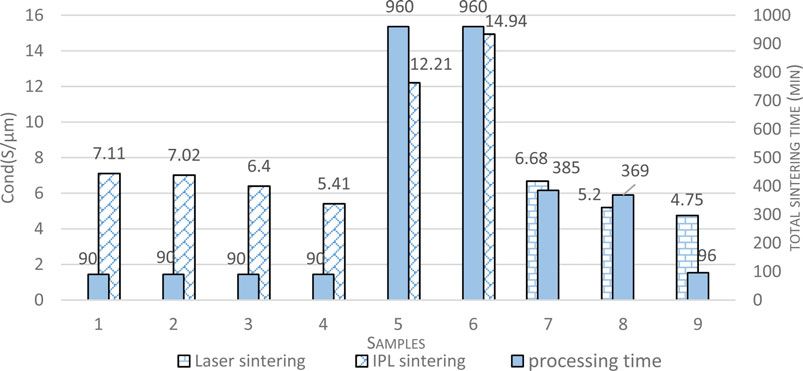
2                                                                                                                                                Chaimaa El Hajjaji et al.

           Especially in the field of printed electronics, heat treatment is                          PI is a flexible polymer substrate that is attracting the
       subdivided into two steps. The first step is drying to evaporate the                       attention of researchers in several fields because of its excellent
       organic substances present in the different inks (solvents, binders,                       mechanical properties and good flexibility, chemical resistance,
       anti-caking agents, etc.) [17]. The second step is sintering, which                        and electrical properties [29, 30]. Its high glass transition tem-
       is crucial for the coalescence between the metal particles to                              perature and thermal resistance (Tg (PI) = 270°C) [22] makes it
       improve the cohesion of the metal deposit and thus obtain                                  an excellent competitor, particularly in low-cost flexible electron-
       good effective conductivity of the deposit [18].                                           ics. For silver deposits printed by direct writing technologies on
           Conventional heat treatment is generally used for resistant                            PI substrates and heat-treated at temperatures between 150 and
       substrates with high glass transition temperatures (alumina,                               220°C, the DC electrical conductivity varies between 22 and
       Rogers, glass, etc.) that can last for hours and reach high                                25 S/μm [27, 28].
       sintering temperatures of up to 1000°C for ceramics, for                                       Most of the literature has focused on DC electrical conductiv-
       example [19].                                                                              ity without providing information on the equivalent electrical
           Andrievski has shown that for identical thermal cycles, the                            conductivity as a function of microwave frequencies, which repre-
       decrease in particle size allows a reduction in the sintering start-                       sents a limiting point for microwave applications.
       ing temperature, which improves the densification kinetics and                                 In this paper, to optimize the performances of microwave pla-
       results in a higher relative density according to the temperature                          nar filters dedicated to demanding applications, such as aerospace
       [11, 19]. This Herring similarity law shows the dependence of                              and defence, we propose to focus on direct printing technologies
       the particle size on the sintering temperature. A more detailed                            with silver ink (IJP and AJP). Standard planar ring resonators that
       dependence is shown in [20]. Because of the nanometric size                                operate in the frequency band (5–21 GHz) on a PI substrate have
       of the metal particles, the sintering temperature has been dras-                           been selected as a representative resonator for these applications.
       tically reduced, which represents a transformation in the field of                             Our research will focus in particular on the improvement of
       printed electronics. At lower thermal sintering temperatures                               the quality factor of this type of planar resonator using alternative
       (200°C) than usual, the electrical conductivity of the metal                               treatment technologies (IPL and laser). This work will be based
       deposit can reach 20 S/μm and higher without damage to the                                 on three main axes. The first axis quantifies the improvement
       metal layer or the substrate used [10].                                                    of the quality factor of these planar resonators during the treat-
           In recent years, the development of printed electronics using                          ment. The second axis consists of improving the ratio between
       polymer substrates has attracted considerable attention due to                             the total treatment time and the quality factor of the planar reso-
       the potential of flexible and low-cost electronic devices. The limit-                      nators. Finally, the last axis presents the technique of extraction of
       ing factor of the most commonly used polymer substrates is their                           the equivalent conductivity of the metallic deposit at different
       low glass transition temperatures (Tg (PLA) = 60°C, Tg (PET) =                             microwave frequencies, which represents one of the particularities
       70°C, Tg (Acrylonitrile Butadiene Styrene (ABS)) = 110°C, Tg                               of our paper.
       (Polyethylene Naphthalate (PEN)) = 120°C, etc.) [21, 22]. After                                This paper is subdivided into two main sections:
       metallization of polymer substrates, alternatives to high-                                     The first section will describe the microwave sample used for
       temperature heat treatment will be used to improve the electrical                          our research (planar microwave resonator), as well as the alterna-
       conductivity of the metal deposits.                                                        tive sintering by IPL or laser and the microwave conductivity
           To solve the constraints related to the sintering of metallic                          extraction technique. Illustrations by SEM (scanning electron
       nanoparticle inks on a flexible support, a large community of                              microscope) and microscopic images of the metal layer after
       researchers and industrialists are interested in the development                           each IPL or laser treatment are also provided. The second section
       of new, selective sintering technologies. These technologies are                           summarizes the results after IPL and laser sintering and the trade-
       mainly based on the concept of sintering only the ink while min-                           off between conductive deposition and reduced processing time.
       imizing the thermal effect with the substrate. We can mention                                  An earlier version of this paper was presented at the
       plasma sintering, fast electrical sintering, and sintering using elec-                     EuMW2020 conference and was published in its Proceedings
       tromagnetic excitation (infrared, laser, and photonic sintering by                         [31]. In this extended version, two additional IPL processing para-
       intense pulsed light (IPL)) [23].                                                          meters are presented accompanied by SEM images of a sectional
           The most commonly used treatments that give relevant results                           view of the metal deposit. A new laser processing technology
       are laser sintering and sintering using short pulses of light, often                       accompanied by SEM images before and after sintering is also
       called intense pulsed light sintering (IPL). The first treatment con-                      added and compared to a previous work proposed at the
       sists of scanning the laser near or on the metal layers [24] to densify                    EuMW2019 conference [32]. All the mentioned results are sum-
       the metal deposit locally and improve electrical conductivity.                             marized in this paper along with the technological parameters
           The second treatment is based on the absorption by the metal-                          and general recommendations needed to reproduce them.
       lic ink of light intensity and its conversion into thermal energy.
       Light is generated by xenon stroboscopic lamps with a wide emis-
       sion spectrum. The light intensity is mainly localized in the visible                      Experiments
       range and corresponds well with the absorption of metallic nano-
                                                                                                  IPL sintering
       particle inks.
           In the state of the art, metallic deposits printed by additive                         IPL sintering consists of using an extremely powerful flash lamp
       technologies (IJP) with average thicknesses of 0.35 μm on poly-                            with a broad and adjustable spectrum, including infrared, visible,
       mer substrates (PET) and treated by laser sintering have DC elec-                          and ultraviolet (UV) light. It sends intense, short pulses of light
       trical conductivities between 4.7 S/μm [25] and 10.4 S/μm [26].                            that are converted into heat to fuse ceramic or metal particles
           For metal deposits printed by IJP with thicknesses between 1                           at room temperature without damaging substrates, which are
       and 10 μm on PI, the DC electrical conductivities are between                              often heat-sensitive (paper, cloth, plastic, thermoplastic, etc.).
       1.2 S/μm [27] and 21 S/μm [28].                                                            This treatment technique saves time and can homogeneously

Downloaded from https://www.cambridge.org/core. IP address: 46.4.80.155, on 27 Apr 2021 at 16:09:32, subject to the Cambridge Core terms of use, available at https://www.cambridge.org/core/terms.
https://doi.org/10.1017/S175907872100043X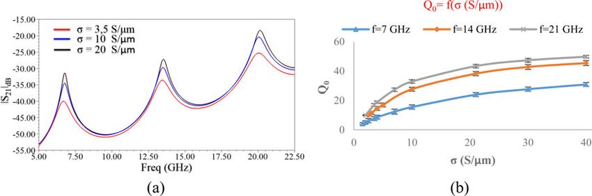
International Journal of Microwave and Wireless Technologies                                                                                                                   3

                                                                                                   thickness was deposited (average value). The resonator is excited
                                                                                                   by a microstrip line of 50 Ω, and finally, a coplanar to microstrip
                                                                                                   transition is used for GSG (ground–signal–ground) probe mea-
                                                                                                   surements of its S parameters. After printing, the samples were
                                                                                                   dried (before photonic sintering) on a hot plate at 200°C for 90
                                                                                                   min to evaporate the solvents that were initially in the silver
                                                                                                   ink. Figure 2(c) shows a thermal image of the resonators during
                                                                                                   drying. The difference in colours on the plate proves the inhomo-
        Fig. 1. Typical profile of the light pulses.                                               geneity of this sintering technique, which leads to slightly differ-
                                                                                                   ent quality factors for the different resonators. After drying on the
                                                                                                   hot plate for 90 min at 200°C, the unloaded quality factors of the
        sinter a metal surface, particularly over large areas. This new tech-                      resonators are between 11 and 16. The equivalent microwave con-
        nique was developed by NovaCentrix in 2006, but it remains less                            ductivities are between 2.8 and 4.5 S/μm at 14 GHz, and the aver-
        widespread than other sintering technologies for microwave                                 age continuous (DC) conductivity is 3.5 S/μm [7]. The samples
        applications.                                                                              will then be sintered with IPL.
            The sintering equipment used in this work is a Xenon X-1100                                Characterization of the printed ink conductivity. The PI sub-
        IPL system that generates precisely controlled light pulses of high                        strate was precisely characterized using a resonant cavity method
        intensity. This system is presented in [31] with more details.                             at three frequencies, and its properties are presented in Table 1.
        Notably, the system cannot deliver the same energy for each                                    The resonant ring presented in part A.1 is used to character-
        light pulse. A typical profile of the train of pulses is shown in                          ize the equivalent electrical conductivity of the printed metal
        Fig. 1. The number of pulses can be selected, as well as their dur-                        layer at microwave frequencies. For conductivities from 3.5 to
        ation (TON) and the time between two pulses (TOFF).                                        40 S/μm, the quality factor value was calculated at three reson-
            The IPL sintering system consists of the following compo-                              ance frequencies (7, 14, and 21 GHz). The results obtained by
        nents: a xenon flash lamp, a reflector, a UV filter, a power supply,                       the simulation with HFSS (high frequency structure simulator)
        capacitors, and a simmer triggering pulse controller. IPL is pro-                          are presented in Fig. 3. Figure 3(a) shows that the improvement
        duced by a plasma arc between the electrodes after the gas is                              of the conductivity leads to higher S21 peak values and to a
        ionized by a voltage bias of 10 kV [33]. When the lamp is trig-                            slight shift of the resonance frequencies of the ring resonator.
        gered using a pulse controller, ∼1000 A of electrical current is                           This behavior is expected in the following measurements. The
        delivered in a few milliseconds from the capacitor.                                        plot of the values of the simulated quality factors (Fig. 3(b))
            The optical spectrum of the light of our xenon lamp ranges in                          allows the estimation of the electrical conductivity of the
        wavelength from 190 to 1100 nm. Because UV light degrades                                  metal deposit. The higher the order of the resonance modes
        polymer substrates, a UV filter has been used to eliminate wave-                           of these ring resonators is, the higher the Q factor will be.
        lengths below 380 nm [34]. Figure 1 represents the real shape of                           Notably, this electromagnetic model gives an equivalent value
        the pulses sent by the xenon lamp. For this example, the capacitor                         of the conductivity of a smooth metal layer at different frequen-
        has been charged by a voltage of 3000 V, and the lamp sends three                          cies and hypothesizes that the metal layer is uniform in thick-
        pulses of identical duration (TON = TOFF = 875 μs). As shown, the                          ness. However, the quality factor of this resonator is a good
        pulses and the voltage at the terminals of the capacitor follow the                        indicator of the quality of the metal layer, particularly when
        same decreasing tendency, which is explained in terms of the dis-                          specific sintering treatments are used to improve the electrical
        charge of the capacitor.                                                                   conductivity of the metal layer and the planar resonator quality
                                                                                                   factor.
        Processing of inkjet-printed samples dried on a hot plate                                      Furthermore, the conductivity extracted from an equivalent
        Based on the work of Rojas-Nastrucci [35], a planar ring reson-                            smooth metal layer decreases as the frequency increases. These
        ator was used to characterize the conductivity of the printed                              phenomena are studied in [36, 37] to characterize and quantify
        metal layer.                                                                               the losses introduced by the dielectric metal interface. In these
           The samples are square ring resonators printed by IJP technol-                          works, more information is given to explain why conductor losses
        ogy, as shown in Fig. 2(a), and are 2 mm long and 226 μm wide                              increase with the frequency. The work in [36] explains more par-
        (Wresonator). Their internal diameter (din) is 6.65 mm to have                             ticularly through equivalent models that the conductor losses
        three resonances at ∼7, 14, and 21 GHz, as shown in Fig. 2(b).                             increase with the frequency, particularly when the skin depth
        On a 125 μm thick PI substrate, a silver metal layer of 1.6 μm                             becomes small compared to the metal surface roughness.

        Fig. 2. Silver ring resonator printed with inkjet on a polyimide substrate (a), representation of the dimensions of the sample (b), and thermal image of the samples
        during drying on the hot plate (c)[31].

Downloaded from https://www.cambridge.org/core. IP address: 46.4.80.155, on 27 Apr 2021 at 16:09:32, subject to the Cambridge Core terms of use, available at https://www.cambridge.org/core/terms.
https://doi.org/10.1017/S175907872100043X
4 Chaimaa El Hajjaji et al.
Table 1. Polyimide substrate characterization at three frequencies. an improvement in the quality factors was observed, which is
justified by the refinement of the transmission peaks. This
fr (GHz) εr tg δ
improvement in the transmission level is a direct consequence
7 3.35 ± 0.035 0.99 × 10⁻² ± 4.13 × 10⁻⁴ of a substantial optimization of the conductivity of the metal
layer. Samples 1−3 do not show substantial physical damage,
14 3.29 ± 0.050 1.06 × 10⁻² ± 3.75 × 10⁻⁴
but sample 4 presents minor damage and therefore changes
21 3.23 ± 0.036 1.13 × 10⁻² ± 2.68 × 10⁻⁴ in its final dimensions after IPL sintering. The latter changes
induced a frequency behavior that is slightly different for its
resonance frequencies and made them shift towards lower fre-
Experimental results. After several preliminary tests with IPL quencies after IPL sintering, contrary to the expected behavior
sintering, it was deduced that distributing the energy of the (Figs 3(a) and 4, samples 1 to 3). The final quality factor and its
lamp over several pulses avoids continuously heating the sample rate of improvement are related to the initial value of the
and an accumulation of heat that can severely damage the poly- quality factor, which varies between samples because of the
mer substrate. As the pulse time decreases, the power of the IPL drying inhomogeneity on the hot plate, as shown in Fig. 2(c).
light increases and can cause cracks and ablations in the metal The most relevant results are obtained from the IPL sintering
layer. Thus, sending the maximum energy of the lamp (E = parameters for the two-pulse sintering case, which corresponds
2433 J/pulse) at a distance of less than 5 cm must be avoided so to sample 2.
that no ablations of the metal layer or deformations of the sub- The electrical conductivity at each resonance frequency is
strate occur. extracted considering the microwave characteristics of the PI sub-
The most relevant IPL sintering parameters, which allow a strate (permittivity and loss tangent) at each resonance frequency.
substantial improvement in the quality factor and the electrical Figure 5 shows top and crosscut SEM images of the metal layers
conductivity, are presented in Table 2. before and after IPL sintering. After drying on the hot plate, the
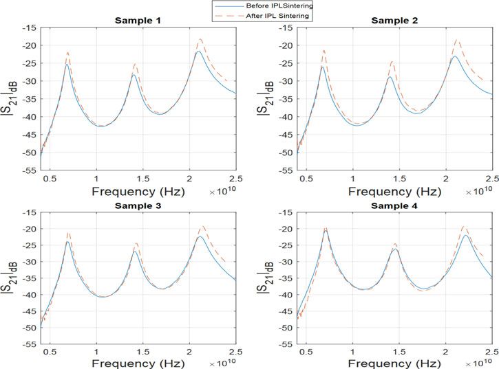
Figure 4 illustrates the measured transmission coefficients metal nanoparticles are small with rare grain boundaries. After
(S21) of the resonators before and after IPL sintering. The mea- IPL sintering, grain boundaries are created between the nanopar-
surements of the quality factor at the three resonant frequen- ticles, inducing a conductive path with less porosity in the
cies, as well as the estimated values of the equivalent microstructure, which is justified by the improved electrical con-
electrical conductivity, are presented in Table 3. After sintering, ductivity of the metal deposit after IPL treatment [38].
Fig. 3. Effect of the electrical conductivity of the metal deposit on the simulated resonator transmission coefficient (a) and evolution of the quality factor of the
printed silver resonator as a function of the conductivity for its first three resonant frequencies (b) (HFSS simulation).
Table 2. IPL sintering parameters used for the optimization of the electrical conductivity.
Energy density
Samples Voltage (V) Number of pulses dLamp (cm) TON (μs) TOFF (μs) (J/pulse)
1 2500 1 5 7000 — Pulse 1 1690
2 2500 2 5 1400 1400 Pulse 1 1274
Pulse 2 371
3 2500 3 5 875 875 Pulse 1 986
Pulse 2 445
Pulse 3 200
4 3000 3 10 875 875 Pulse 1 1420
Pulse 2 641
Pulse 3 289
Downloaded from https://www.cambridge.org/core. IP address: 46.4.80.155, on 27 Apr 2021 at 16:09:32, subject to the Cambridge Core terms of use, available at https://www.cambridge.org/core/terms.
https://doi.org/10.1017/S175907872100043XInternational Journal of Microwave and Wireless Technologies 5
Fig. 4. Measurements of resonator S21 before and
after IPL sintering for samples 1, 2, 3, and 4.
Table 3. Quality factor measurements before and after sintering and extraction of estimated microwave conductivity values.
Frequency 7 GHz 14 GHz 21 GHz
Sample 1 Before sintering Q0 11.9 ± 0.64 16.2 ± 0.53 18.9 ± 0.55
σ (S/μm) 6 ± 0.14 4.56 ± 0.12 3.8 ± 0.11
After sintering Q0 16.7 ± 0.70 22.7 ± 0.6 25.6 ± 0.50
σ (S/μm) 11.3 ± 0.18 7.11 ± 0.15 5.9 ± 0.15
% improvement of Q0 40% 40% 35%
Sample 2 Before sintering Q0 10.6 ± 0.35 14.5 ± 0.51 16.3 ± 0.19
σ (S/μm) 5 ± 0.15 3.98 ± 0.12 3.14 ± 0.11
After sintering Q0 17 ± 0.74 22.5 ± 0.80 24.8 ± 0.50
σ (S/μm) 11.9 ± 0.25 7.02 ± 0.12 5.61 ± 0.15
% improvement of Q0 60% 55% 52%
Sample 3 Before sintering Q0 10,3 ± 0.32 14.8 ± 0.51 16.4 ± 0.19
σ (S/μm) 4.8 ± 0.14 4.08 ± 0.13 3.16 ± 0.11
After sintering Q0 15 ± 0.73 21.1 ± 0.75 22 ± 0.45
σ (S/μm) 9.26 ± 0.19 6.4 ± 0.11 469 ± 0.12
% improvement of Q0 46% 43% 34%
Sample 4 Before sintering Q0 10.7 ± 0.35 13.2 ± 0.35 17.9 ± 0.55
σ (S/μm) 5.13 ± 0.16 3.54 ± 0.12 3.54 ± 0.11
After sintering Q0 16 ± 0.70 18.6 ± 0.7 23.2 ± 0.52
σ (S/μm) 10.3 ± 0.19 5.41 ± 0.12 5.1 ± 0.12
% improvement of Q0 50% 41% 30%
Processing of aerosol jet printed and oven-dried samples and the resonator sizes are Wresonator = 225 μm and din = 8.22
In this section, we again consider samples that are square ring mm. In this case, their first three resonances are at 5, 10, and
resonators on the PI substrate but printed this time by AJP 15 GHz. After printing, the test patterns were dried in an oven
[10]. The average thickness of the printed silver ink is 0.8 μm, to avoid the constraint of inhomogeneous drying of the samples
Downloaded from https://www.cambridge.org/core. IP address: 46.4.80.155, on 27 Apr 2021 at 16:09:32, subject to the Cambridge Core terms of use, available at https://www.cambridge.org/core/terms.
https://doi.org/10.1017/S175907872100043X6 Chaimaa El Hajjaji et al.
Fig. 5. Top and cross-section SEM images of metal deposits after drying on the hot plate (a, top view only) [31] and after IPL sintering of sample 1 (b), sample 2 (c),
sample 3 (d), and sample 4 (e).
Table 4. IPL sintering parameters used for the optimization of the electrical conductivity.
Energy density
Samples Voltage (V) Number of pulses dLamp (cm) TON (μs) TOFF (μs) (J/pulse)
5 2500 1 5 7000 — Pulse 1 1690
6 3000 6 10 438 438 Pulse 1 864
Pulse 2 575
Pulse 3 383
Pulse 4 255
Pulse 5 170
Pulse 6 114
on the heating plate, as illustrated by the thermal images nanoparticles below the surface layer are sintered by heat transfer
(Fig. 2(c)) in part A.1. The silver ink was dried following a heating from the top surface of the metal layer. At the same time, the ther-
ramp from 30 to 180°C. After this ramp, the samples were heated mal decomposition of organic additives inside the silver film
for 60 min at 180°C. IPL sintering was then applied after this first induces vaporization. However, once the metal layer is formed
drying step. Samples S21, unloaded Q factors and extracted on the surface of the film, the internal gases are not easily evapo-
equivalent conductivities at microwave frequencies were measured rated, which could cause the film to swell during reflow of the sur-
as explained previously. After the ink drying step, which lasted face metal layer in the second or third light irradiation, as
16 h, IPL was used to improve the conductivity of the conductive explained in [5]. As seen in [31], this result leads to a small dwell-
deposit. The most relevant IPL sintering parameters used, as well ing for samples 2 and 3. In sample 4, we notice that burnt areas
as the characterization of the microwave conductivity, are are at the level of the metal layer because of the extremely short
presented in Tables 4 and 5, respectively. time between the pulses (Toff = 438 μs), which did not allow suffi-
Figure 6 shows the top SEM images of the metal layer after cient cooling time for the metal deposit. The observed local
oven drying and IPL sintering. After sintering in the oven, the deformation does not substantially change the microwave behav-
nanoparticles started to densify, creating grain boundaries ior of the resonators. However, complementary tests are needed to
between them. IPL sintering allowed minimization of the pores check the adhesion quality of the silver layer on the PI substrate.
between the nanoparticles to create a conductive path between
the particles. The measured S21 values of samples 5 and 6 before
Laser sintering
and after IPL sintering are similar to the plots presented in Fig. 4.
When the energy of the lamp is divided into several pulses, the Unlike most alternative sintering techniques (hot plate, oven,
energy of the first pulse is absorbed mainly by the upper surface UV, or IR sintering), laser sintering is a selective, fast, and loca-
of the film. When the other pulses are applied consecutively, the lized sintering process. It consists of sintering the metal deposit
Downloaded from https://www.cambridge.org/core. IP address: 46.4.80.155, on 27 Apr 2021 at 16:09:32, subject to the Cambridge Core terms of use, available at https://www.cambridge.org/core/terms.
https://doi.org/10.1017/S175907872100043XInternational Journal of Microwave and Wireless Technologies 7
Table 5. Quality factor measurements before and after sintering and extraction of estimated microwave conductivity values.
Frequency 5 GHz 10 GHz 15 GHz
Sample 5 Before sintering Q0 9.9 ± 0.42 14.3 ± 0.45 18.3 ± 0.48
σ (S/μm) 11 ± 0.30 8.37 ± 0.12 7.6 ± 0.15
After sintering Q0 14 ± 0.39 19.8 ± 0.50 24.4 ± 0.50
σ (S/μm) 19.4 ± 0.35 13.4 ± 0.12 11.8 ± 0.14
% improvement of Q0 41% 38.5% 33%
Sample 6 Before sintering Q0 13 ± 0.37 19.5 ± 0.50 24.8 ± 0.50
σ (S/μm) 17.1 ± 0.40 13.1 ± 0.12 12.2 ± 0.11
After sintering Q0 14.5 ± 0.39 22.2 ± 0.55 27.3 ± 0.53
σ (S/μm) 20.6 ± 0.30 16 ± 0.15 14.4 ± 0.14
% improvement of Q0 11.5% 14% 10%
Fig. 6. SEM images of the silver surface after drying (a) and after IPL sintering (b; samples 5 and c; sample 6).
Table 6. Summary of the results of three laser sintering techniques.
Frequency 5 GHz 10 GHz 15 GHz
Sample 7: Hatching technique Before sintering Q0 8.7 ± 0.18 11.6 ± 0.02 15 ± 0.04
σ (S/μm) 5.37 ± 0.43 3.48 ± 0.53 3.83 ± 0.12
After 24 passes Q0 13 ± 0.39 18.4 ± 0.06 20.5 ± 0.08
σ (S/μm) 9.23 ± 0.35 6.3 ± 0.59 6.48 ± 0.39
% improvement of Q0 50% 59% 37%
Sample 8: Rectangle technique Before sintering Q0 7.8 ± 0.15 10.3 ± 0.04 11.5 ± 0.03
σ (S/μm) 4.64 ± 0.42 3.11 ± 0.4 2.75 ± 0.12
After 40 passes Q0 13 ± 0.39 17.2 ± 0.11 17.3 ± 0.06
σ (S/μm) 9.23 ± 0.35 5.74 ± 0.5 5 ± 0.4
% improvement of Q0 67% 67% 51%
Sample 9: Square technique Frequency 7 GHz 14 GHz 21 GHz
Before sintering Q0 7.3 ± 0.20 10.9 ± 0.32 12.1 ± 0.19
σ (S/μm) 3.28 ± 0.14 2.81 ± 0.10 2.41 ± 0.10
After 40 passes Q0 11 ± 0.30 16.39 ± 0.45 18 ± 0.48
σ (S/μm) 5.87 ± 0.13 4.72 ± 0.12 3.81 ± 0.12
% improvement of Q0 51% 50% 49%
using a laser beam at a fixed wavelength in continuous or pulsed spot diameter equal to 100 μm (using a focal distance of 3 mm)
mode. and to avoid damage to the polymer substrate. The scanning
In our research, an infrared laser that sends pulses at the fre- speed of the laser can be set between 1 and 100 mm/s, and its
quency f = 40 kHz at λ = 1064 nm is used to sinter similar inkjet maximum output power is 20 W by selecting the intensity of
printed ring resonators. The laser was defocused to provide a the laser current source (0–50 A).
Downloaded from https://www.cambridge.org/core. IP address: 46.4.80.155, on 27 Apr 2021 at 16:09:32, subject to the Cambridge Core terms of use, available at https://www.cambridge.org/core/terms.
https://doi.org/10.1017/S175907872100043X8 Chaimaa El Hajjaji et al.
Fig. 7. Measurements of sample 9 before and after 40 laser passes (a) and improvement of the conductivity according to the number of laser passes (b).
Fig. 8. Cross-section SEM images of the metal layer after 40 laser passes (a, b) and microscopic top image of the edge of the resonator after the laser passes (c).
Fig. 9. Final electrical conductivity of the metal deposit after laser or IPL treatment as a function of the total sintering time at f = 14 GHz.
Description of the sintering methods there is a maximum strength of magnetic fields to provide excel-
The laser sintering of inkjet printed resonators has already been lent current conductivity. The first two techniques, i.e. the hatch-
tested with two methods [32], and a third method is proposed ing and rectangular techniques, are described in [32].
in this section. Considering the noticeably long total sintering time (drying
After printing the samples, they were dried at 200°C for 6 h on and laser sintering) for these two previous techniques, we intend
a hot plate to evaporate the solvents present in the ink. to reduce the drying time on the hot plate to 90 min, as well as the
The three selective sintering techniques consist of passing the laser sintering time, by proposing a third technique that we call
laser only over the metal layer to increase its conductivity without the square technique. It is inspired by [35] and consists of scan-
damaging the polymer substrate near and beneath it. ning the sample with the laser passing on the edges of the reson-
The common point between these three techniques is the pas- ator. For the other two sintering methods, the laser beam was
sage of the laser beam on or near the edges of the resonator where defocused to avoid damage to the polymer substrate. For the
Downloaded from https://www.cambridge.org/core. IP address: 46.4.80.155, on 27 Apr 2021 at 16:09:32, subject to the Cambridge Core terms of use, available at https://www.cambridge.org/core/terms.
https://doi.org/10.1017/S175907872100043XInternational Journal of Microwave and Wireless Technologies 9
square method, we used 8% laser power with a scanning speed of For IPL sintering, this technique distributes the energy emitted
10 mm/s. The sintering time is 6 min after 40 laser passes. by the lamp evenly over the metal deposit. It can treat many metal
patterns printed on a substrate at the same time. In addition, the
Experimental results extremely short duration (ms) of the light pulses and the width of
Table 6 provides the measured unloading Q factors and the their spectrum covering the UV, visible, and IR regions (190–
extracted equivalent conductivity before and after the laser sinter- 1100 nm) allow it to treat all types of metals and substrates.
ing step with the three proposed techniques (hatching, rectangle, The ratio between this quick sintering step (a few ms) that follows
and square). a conventional drying step (hot plate or oven) and the percentage
S parameter measurements and equivalent conductivity extrac- of improvement of the Q factor of the printed planar resonators at
tion are performed for 10, 20, 30, and 40 passes of the laser with microwave frequencies is excellent.
the square technique (Fig. 7(a)). Laser sintering is a relevant alternative technique. It is a localized
The main improvement in the conductivity is after the first 10 annealing step in which the laser can selectively sinter printed metal
passes because, as shown in Fig. 7(b), the electrical conductivity of patterns without damaging the underlying polymer substrate or the
the deposit becomes saturated. nearby components. Lasing times between 6 and 25 min are
According to the microstructural distribution (MD), we required depending on the selected lasing strategy, which leads to
noticed that the nanoparticles melted and created grain boundar- an improvement of the planar resonator unloaded Q factor of up
ies between themselves, which made it possible to build conduct- to +51% at 14 GHz. As a direct consequence, if we consider a
ive paths (Figs 8(a) and 8(b)). Because the laser is localized fourth-order Chebyshev filter made with these resonators, having
sintering, the MD is not homogeneous over the entire metal a central frequency of 14 GHz, a bandwidth of 2.8 GHz and a return
deposit, which is illustrated by the red arrows and can be repre- loss of 20 dB, the proposed sintering techniques would provide an
sented as traps for the nanoparticles. improvement of its insertion losses of up to 2.5 dB.
Microscopic images of the sample after the laser treatment Therefore, the use of these sintering techniques in the field of
(Fig. 8(c)) show no ablation and no damage to the polymer sub- printed electronics, particularly for sintering printed microwave
strate or the metal layer. Therefore, laser sintering can be consid- planar components on low melting temperature polymer sub-
ered a localized sintering technique that improves the electrical strates, seems to be a relevant, complementary technique to con-
conductivity without damaging the deposit if the proper lasing ventional methods. For our future works, we will consider other
parameters are applied. polymer substrates, such as PEEK (tg = 152°C), which is widely
Table 6 summarizes the improvement of the quality factor and used in the aeronautics domain, over a broader range of passive
equivalent electrical conductivity extraction of the metal deposit components, such as microwave filters, transmission lines (micro-
of the resonators before and after each laser sintering technique. strip, CPW), or antennas.
The three sintering techniques allow a substantial improve-
Acknowledgements. The authors thank their colleagues from the Institute
ment of the quality factor and electrical conductivity. The hatch-
for Research on Ceramics (IRCER, Limoges) and, more specifically, Mr. Pierre
ing technique allows the entire metal surface to be sintered but
Carles for his great support with the SEM images of the metal layers.
with a long sintering time (25 min), and the rectangle technique
achieves almost identical quality factor values as those of the
hatching technique in less treatment time (9 min). The square References
technique represents the trade-off between improving the final
1. Borghetti M, Cantù E, Sardini E and Serpelloni M (2020) Future sensors
quality factor and reducing the total sintering time (6 min). for smart objects by printing technologies in industry 4.0 scenario.
Because extractions were performed at different frequencies, Energies 13, Art. no. 22. doi: 10.3390/en13225916
our conclusions are based on the data that are used to estimate 2. Cruz S, Rocha L and Viana J (2018) ‘Printing Technologies on Flexible
the conductivity of each case at 14 GHz. Substrates for Printed Electronics’.
Figure 9 presents the final electrical conductivity of the metal 3. Seifert T, Sowade E, Roscher F, Wiemer M, Gessner T and Baumann
deposit at f = 14 GHz after the IPL or laser treatment, considering RR (2015) Additive manufacturing technologies compared: morphology
the total treatment time (drying and sintering). Note that to achieve of deposits of silver ink using inkjet and aerosol jet printing. Industrial
high conductivity values (σ > 12 S/μm, typically), the total treatment & Engineering Chemistry Research 54, 769–779.
time must be long (16 h) and to reduce the treatment time (∼90 4. Baron S (2015) ‘Flexible polymer for X-band electrically tunable patch
antenna: design and characterizations’, Theses, Université de Nantes.
min), the final equivalent conductivity is ∼3.8–7.1 S/μm.
5. Mitra KY, Alalawe A, Voigt S, Boeffel C and Baumann RR (2018)
Manufacturing of all inkjet-printed organic photovoltaic cell arrays and
Conclusion evaluating their suitability for flexible electronics. Micromachines 9, Art.
no. 12. doi: 10.3390/mi9120642
To improve the low conductivity of a given silver ink (3–4.5 S/μm) 6. Rao Balakrishnan S and Asri M (2014) Conventional photolithography
by improving the deposit conductivity, two sintering techniques and process optimization of pattern-size expansion technique for nanogap
have been studied. Accompanied by detailed microscopic views, biosensor fabrication. Advanced Materials Research 832, 89–94.
unloaded Q factor and equivalent conductivity measurements 7. Abdelghani A (2018) ‘Microwave gas sensor based on carbon nanotubes,
between 5 and 21 GHz, a study of microwave ring resonator sam- printed by inkjet technology’, Doctoral thesis, Limoges.
ples was performed for different sintering treatments to determine 8. Macuri CAP ‘Design of radio-frequency gas sensors based on carbon
nanotubes and inkjet printing’, p. 276.
the strengths and weaknesses of each method.
9. Lee H, Seo S, Yun K, Joung JW, Oh I and Yook J (2008) ‘RF
A maximum equivalent electrical conductivity of 14.49 S/μm Performance of CPW transmission line fabricated with inkjet printing
after IPL sintering and of 6.5 S/μm [32] after laser sintering are technology’, in 2008 Asia-Pacific Microwave Conference, Dec. 2008, pp.
obtained at f = 14 GHz. Because of these unconventional sintering 1–4, doi: 10.1109/APMC.2008.4958022.
methods, the unloaded Q factors of silver-printed planar resona- 10. Delage A (2019) ‘Aerosol technology applied to 3D integration and micro-
tors show an improvement of up to + 55% (with IPL sintering). wave components’, Doctoral thesis, Limoges.
Downloaded from https://www.cambridge.org/core. IP address: 46.4.80.155, on 27 Apr 2021 at 16:09:32, subject to the Cambridge Core terms of use, available at https://www.cambridge.org/core/terms.
https://doi.org/10.1017/S175907872100043X10 Chaimaa El Hajjaji et al.
11. Florent G ‘Additive manufacturing of electroactive materials for mecha- 32. Hajjaji CE, George J, Lmansouri S, Delhote N, Verdeyme S, Baillargeat
tronics applications’, p. 134. D, Piechowiak M and Durand O (2019) ‘Optimizing the conductivity of
12. Hu A, Guo JY, Alarifi H, Patane G, Zhou Y, Compagnini G and Xu CX ink-jet printed microwave components on polymer substrates by laser sin-
(2010) Low temperature sintering of Ag nanoparticles for flexible electron- tering’, in 2019 49th European Microwave Conference (EuMC), Oct. 2019,
ics packaging. Applied Physics Letters 97, 153117. pp. 778–781, doi: 10.23919/EuMC.2019.8910768.
13. Minari T, Kanehara Y, Liu C, Sakamoto K, Yasuda T, Yaguchi A, Tsukada 33. ‘Flash lamp Eg&G.pdf’, Available at https://www.flashlamps-vq.com/
S, Kashizaki K and Kanehara M (2014) ‘Room-Temperature Printing of CatalogueVQF.pdf.
Organic Thin-Film Transistors with π-Junction Gold Nanoparticles – 34. Mittal KL (2005) Polyimides and Other High Temperature Polymers: Synthesis,
Minari – 2014 – Advanced Functional Materials – Wiley Online Library’. Characterization and Applications, held in Orlando, December 17-19, 2003
14. Joo S-J, Hwang H-J and Kim H-S (2014) Highly conductive copper 35. Rojas-Nastrucci EA (2017) Characterization and modeling of K-band
nano/microparticles ink via flash light sintering for printed electronics. coplanar waveguides digitally manufactured using pulsed picosecond
Nanotechnology 25, 265601. laser machining of thick-film conductive paste. IEEE Transactions on
15. Xu H, Tang X, Sun H, Zhao H and Li M (2017) ‘Conductivity of silver Microwave Theory and Techniques 65, 3180–3187.
and copper film printed by particle-free reactive inks’, in 2017 18th 36. Méndez-Jerónimo G, Sejas-García SC and Torres-Torres R (2018)
International Conference on Electronic Packaging Technology (ICEPT), Modeling and parameter extraction for the metal surface roughness loss
Harbin, China, Aug. 2017, pp. 1470–1473, doi: 10.1109/ICEPT.2017.8046713. effect on substrate integrated waveguides from S-parameters. IEEE
16. Sarkar SK, Gupta H and Gupta D (2016) ‘Flash light sintering of silver Transactions on Microwave Theory and Techniques 66, 875–882.
ink for inkjet printed organic thin film transistor on flexible substrate’, in 37. Ding R, Braunisch H, Tsang L and Chang W (2012) ‘Simulation and
2016 3rd International Conference on Devices, Circuits and Systems measurement correlation of random rough surface effects in intercon-
(ICDCS), Mar. 2016, pp. 68–72, doi: 10.1109/ICDCSyst.2016.7570627. nects’, in 2012 IEEE 21st Conference on Electrical Performance of
17. Wang Z, Zhao T, Liang X, Zhu P and Sun R (2017) ‘A low cost method Electronic Packaging and Systems, Oct. 2012, pp. 272–275, doi: 10.1109/
to synthesize silver nanoparticles for the screen printing conductive inks’, EPEPS.2012.6457894.
in 2017 18th International Conference on Electronic Packaging Technology 38. Greer JR and Street RA (2007) Thermal cure effects on electrical per-
(ICEPT), Aug. 2017, pp. 1121–1124, doi: 10.1109/ICEPT.2017.8046638. formance of nanoparticle silver inks. Acta Materialia 55, 6345–6349.
18. Moon K-S, Dong H, Maric R, Pothukuchi S, Hunt A, Li Y and Wong
CP (2005) Thermal behavior of silver nanoparticles for low-temperature Chaimaa El Hajjaji received a master’s degree in
interconnect applications. Journal of Electronic Materials 34, 168–175. High Technologies, Electronics, and Photonics
19. Ndayishimiye A ‘On a new low-temperature ceramic sintering process: from the University of Limoges, France, in
hydrothermal sintering. Development and mechanistic approach’, p. 213. 2018. She is now a Ph.D. candidate with the
20. Herring C (1950) Effect of change of scale on sintering phenomena. MACAO team in the XLIM Laboratory in col-
Journal of Applied Physics 21, 301–303. laboration with the Centre for Technology
21. Rieger J (2000) ‘Glass Transition Temperature (Tg) of Plastics - Definition Transfers in Ceramics (CTTC) at Limoges.
& Values’. Available at https://omnexus.specialchem.com/polymer-properties/ Her research interests mainly focus on the
properties/glass-transition-temperature. design of microwave components and the
22. Khan S, Dahiya R and Lorenzelli L (2014) Technologies for printing sen- improvement of their performance using emerging sintering techniques.
sors and electronics over large flexible substrates: a review. IEEE Sensors
Journal. doi: 10.1109/JSEN.2014.2375203. Dr. Nicolas Delhote received his Ph.D. in 2007
23. Baudino O ‘Photonic sintering of printed lines based on nanoparticles: from the University of Limoges, France. He is
optimization of electrical and mechanical properties for the interconnec- the head of the MACAO research group dedi-
tion of integrated circuits on flexible substrates’, p. 191. cated to the design, optimization and fabrication
24. Lopes AJ, Lee IH, MacDonald E, Quintana R and Wicker R (2014) Laser of microwave components. His main activities
curing of silver-based conductive inks for in situ 3D structural electronics are related to advanced manufacturing tech-
fabrication in stereolithography. Journal of Materials Processing nologies (additive manufacturing) and materials
Technology 214, 1935–1945. and to the design and optimization of passive
25. Kim M-K, Hwang JY, Kang H, Kang K, Lee S-H and Moon S-J (2009) microwave components (filters, power dividers,
‘Laser sintering of the printed silver ink’, in 2009 IEEE International etc.) for space and defence applications.
Symposium on Assembly and Manufacturing, Nov. 2009, pp. 155–158,
Dr. Serge Verdeyme received a Ph.D. from the
doi: 10.1109/ISAM.2009.5376912.
University of Limoges, Limoges, France, in 1989.
26. Kim M-K, Kang H, Kang K, Lee S-H, Hwang JY, Moon Y and Moon S-J
(2010) ‘Laser sintering of inkjet-printed silver nanoparticles on glass and He is currently a professor at XLIM, Laboratory
of the CNRS and the University of Limoges, and
PET substrates’, in 10th IEEE International Conference on Nanotechnology,
Aug. 2010, pp. 520–524, doi: 10.1109/NANO.2010.5697913. works in the RF System Department. His primary
27. Lee DJ, Park SH, Jang S, Kim HS, Oh JH and Song YW (2011) Pulsed field of interest concerns the design and optimiza-
tion of microwave components.
light sintering characteristics of inkjet-printed nanosilver films on a polymer
substrate. Journal of Micromechanics and Microengineering 21, 125023.
28. Kang JS, Ryu J, Kim HS and Hahn HT (2011) Sintering of inkjet-printed
silver nanoparticles at room temperature using intense pulsed light.
Journal of Electronic Materials 40, 2268. Dr. Malgorzata Anna Piechowiak has got dou-
29. Krebs FC (2009) Fabrication and processing of polymer solar cells: a ble Ph.D. in Materials Science and Ceramic
review of printing and coating techniques. Solar Energy Materials and Processing at the University of Limoges
Solar Cells 93, 394–412. (France) and Physics of Matter at the
30. Sun Y and Rogers JA (2007) Inorganic semiconductors for flexible elec- University of Genoa (Italy) in 2011. She has
tronics. Advanced Materials 19, 1897–1916. over 8 years of international research experience
31. Hajjaji CE, Delhote N, Verdeyme S, Piechowiak M and Durand O in ceramic engineering (powder synthesis, for-
(2021) ‘Optimization of the conductivity of microwave components mulation of dispersions and pastes, additive
printed by inkjet on polymeric substrates by photonic sintering’, in 2020 manufacturing, film deposition, etc.). Presently,
50th European Microwave Conference (EuMC), Jan. 2021, pp. 380–383, she occupies R&D manager position in the Centre for Technology Transfers
doi: 10.23919/EuMC48046.2021.9338007. in Ceramics (CTTC) and works on projects linked with the development of
Downloaded from https://www.cambridge.org/core. IP address: 46.4.80.155, on 27 Apr 2021 at 16:09:32, subject to the Cambridge Core terms of use, available at https://www.cambridge.org/core/terms.
https://doi.org/10.1017/S175907872100043XInternational Journal of Microwave and Wireless Technologies 11
ceramic-based functional parts by additive manufacturing processes such as experience to set up and carry out European projects and the dissemination
binder jetting, aerosol jet, or inkjet printing. of results.
Eng. Laurence Boyer has a technical back- Dr. Olivier Durand received his Ph.D. at the
ground in chemistry and materials. She has University of Limoges in 2006 after fundamental
15 years of experience in the ceramic industry research work on the crystallography of tellur-
acquired in France, Spain in the UK. She ium oxides. After a 3-year postdoctoral fellow-
joined the Centre for Technology Transfers ship on ceramic processes, he joined the
in Ceramics (CTTC) at Limoges in 2018 as Centre for Technology Transfers in Ceramics
the head of Resourcing and Technologies (CTTC) at Limoges in 2009, working as a pro-
Department for defining and monitoring the ject manager for 5 years and then as the
collaborative research and scientific resourcing Materials and Processes Department manager
activities. She is in charge of a team composed of doctors, engineers, and for 3 years. He has registered one patent and has collaborated on five research
technicians working on the development of new materials and manufactur- articles. He is currently the CEO of CTTC, a Research and Technology
ing processes of technical ceramics. She also uses her international Organization specializing in ceramic materials and the processes thereof.
Downloaded from https://www.cambridge.org/core. IP address: 46.4.80.155, on 27 Apr 2021 at 16:09:32, subject to the Cambridge Core terms of use, available at https://www.cambridge.org/core/terms.
https://doi.org/10.1017/S175907872100043XYou can also read