PHOTONIC CONVOLUTION NEURAL NETWORK BASED ON INTERLEAVED TIME-WAVELENGTH MODULATION
←
→
Page content transcription
If your browser does not render page correctly, please read the page content below
P HOTONIC C ONVOLUTION N EURAL N ETWORK B ASED ON
                                                  I NTERLEAVED T IME -WAVELENGTH M ODULATION

                                                                      Yue Jiang, Wenjia Zhang*, Fan Yang, and Zuyuan He
arXiv:2102.09561v1 [cs.ET] 18 Feb 2021

                                                          State Key Laboratory of Advanced Optical Communication Systems and Networks,
                                                                       Shanghai Jiao Tong University, Shanghai, China 200240
                                                                                  *wenjia.zhang@sjtu.edu.cn

                                                                                            February 22, 2021

                                                                                              A BSTRACT
                                                  Convolution neural network (CNN), as one of the most powerful and popular technologies, has
                                                  achieved remarkable progress for image and video classification since its invention in 1989. How-
                                                  ever, with the high definition video-data explosion, convolution layers in the CNN architecture will
                                                  occupy a great amount of computing time and memory resources due to high computation com-
                                                  plexity of matrix multiply accumulate operation. In this paper, a novel integrated photonic CNN is
                                                  proposed based on double correlation operations through interleaved time-wavelength modulation.
                                                  Micro-ring based multi-wavelength manipulation and single dispersion medium are utilized to real-
                                                  ize convolution operation and replace the conventional optical delay lines. 200 images are tested
                                                  in MNIST datasets with accuracy of 85.5% in our photonic CNN versus 86.5% in 64-bit computer.
                                                  We also analyze the computing error of photonic CNN caused by various micro-ring parameters,
                                                  operation baud rates and the characteristics of micro-ring weighting bank. Furthermore, a tensor
                                                  processing unit based on 4 × 4 mesh with 1.2 TOPS (operation per second when 100% utilization)
                                                  computing capability at 20G baud rate is proposed and analyzed to form a paralleled photonic CNN.

                                         1 Introduction
                                         As the driving force of Industry 4.0, artificial intelligence (AI) technology is leading dramatic changes in many spheres
                                         such as vision, voice and natural language classification [1]. Convolution neural networks (CNN), as one of the
                                         most powerful and popular technologies, has achieved remarkable progress for image classification through extracting
                                         feature maps from thousands of images [2]. In particular, CNN, with various structures such as AlexNet [2], VGG16
                                         (or 19) [3] and GoogleNet [4], is mainly consisted of two parts: convolution feature extractors to extract the feature
                                         map through multiple cascaded convolution layers, and fully connected layers as a classifier. In the CNN architecture,
                                         convolution layers will occupy most of computing time and resources [5] due to high computation complexity of
                                         multiply accumulate operation and matrices multiply accumulate operation (MMAC) [6]. Therefore, image to column
                                         algorithm combined with general matrix multiplication (GeMM) [7, 8] and Winograd algorithms [9] were proposed to
                                         accelerate the original 2-D convolution operation (2Dconv) due to the improvement of memory efficiency [10]. With
                                         the high definition video-data explosion, algorithm innovation can not achieve outstanding performance gain without
                                         hardware evolution. Therefore, innovative hardware accelerators have been proposed and commercialized in the forms
                                         of application specific integrated circuit (ASIC) [11], graphics processing unit (GPU) [12, 13] and tensor processing
                                         unit (TPU) [14]. However, it has become overwhelmed for conventional electronic computing hardware to adapt the
                                         continuedly developing CNN algorithm [15].
                                         In the meantime, integrated photonic computing technology presents its unique potential for the next generation high
                                         performance computing hardware due to its intrinsic parallelism, ultrahigh bandwidth and low power consumption
                                         [16]. Recently, significant progress have been achieved in designing and realizing integrated optical neural networks
                                         (ONN) [17, 18, 19]. The fundamental components including Mach-Zehnder interferometers (MZI) [18] and micro-
                                         ring resonators (MRR) [19] have been widely employed to compose a optical matrix multiplier unit (OM2 U), which
                                         is used to complete the MMAC operation. In order to construct full CNN architecture, electrical control unit like field
                                         programmable gate array (FPGA) is required to send slices of input images as voltage control signals to optical modu-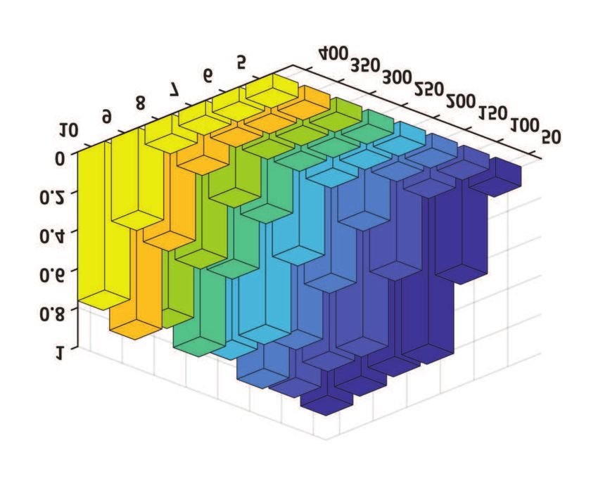
A   PREPRINT   - F EBRUARY 22, 2021

lators and also operate nonlinear activation. For instance, an OM2 U controlled by FPGA, has been proposed by using
fan-in-out structure based on microring resonators [20]. Similarly, CNN accelerator based on Winograd algorithm in
the work of [21] is also composed of an OM2 U based on MRR and electronic buffer. However, the proposed photonic
CNN architecture controlled by electronic buffer rely on electrical components for repeatedly accessing memory to
extract the corresponding image slices (or slice vectors) and are finally constrained by memory access speed and ca-
pacity. In 2018, photonic CNN using optical delay line to replace the electronic buffer was firstly proposed in [22].
Based on the similar idea, the researchers have developed an optical patching scheme to complete the 2-D convolution
in [23], where the wavelength division multiplexing (WDM) method is used[22].
In our previous work [24], wavelength domain weighting based on interleaved time-wavelength modulation was
demonstrated to complete the MMAC operation. The idea of multi-wavelength modulation and dispersed time de-
lay can realize matrix vector multiplication by employing time and wavelength domain multiplexing. However, the
cross-correlation operation between an input vector and a single column of weighting matrix is operated through sam-
pling process by generating a large amount of useless data. Moreover, a 2Dconv operation can be decomposed as
the sum of multiple double correlation operations between vectors. In this paper, a novel integrated photonic CNN
is proposed based on double correlation operation through interleaved time-wavelength modulation. Microring based
multi-wavelength manipulation and single dispersion medium are utilized to realize convolution operation and replace
the conventional optical delay lines used in [22] and [23]. 200 images are tested in MNIST datasets with accuracy
of 85.5% in our PCNN versus 86.5% in 64-bit computer. We also analyze the error of PCNN caused by high baud
rate and the characteristics of MRR weighting bank. Furthermore, a tensor processing unit based on 4 × 4 OM2 U
mesh with 1.2 TOPS (operation per second when 100% utilization) computing capability at 20G baud rate for MZM
architecture is proposed and analyzed to form a paralleled photonic CNN.

2 Physical Implementation of the OCU

2.1 Optical Convolution Unit

The convolution layer is the key building block of a convolution network that operates most of the computational
heavy lifting. Convolution operation essentially performs dot products between the feature map and local regions of
the input. This operation will be iterated in the input image at stride of given location along both width and height.
Therefore, the designed operation will consume a lot of memory, since some values in the input volume are replicated
multiple times due striding nature of this process.
In the proposed photonic CNN as shown in Fig. 1(a), the optical convolution unit (OCU) is consisted of OM2 U and
dispersed time delay unit (TDU). The single 2Dconv operation for the M × M input image A and N × N convolution
kernel w is executed during one period in the OCU, which can be written as:
                                                   N X
                                                   X N
                                         Ym,n =              (wi,j · Am+i−1,n+j−1 )                                   (1)
                                                   i=1 j=1

Here we set M = 3, N = 2 for example in Fig. 1(b), the input image A is flattened into a normalized 1 × M 2 vector
A′ which is modulated by a MZI modulator on multi-wavelength optical signals with N 2 wavelengths: λ1 , λ2 ... λN 2
at certain Baud Rate (marked as BR in equations). The intensity of each frequency after modulation, IA′ (t) can be
written as

                                         M P
                                         P M
                             IA′ (t) =             Iinput · Al,k · Square(t)
                                         l=1 k=1                                                                      (2)
                                                      (l−1)×M+k                (l−1)×M+k+1
                             Square(t) = U [t −           BR    ]   − U [t −        BR     ]
Where the U (t) is the step function, and the Iinput is the intensity of a single channel in WDM sources, which are
equal for all frequencies. Optical signals of different wavelengths are separated by the DEMUX, and sent to the
corresponding MRRs. There are N 2 MRRs R1 ,R2 , . . . , RN 2 compose as a MRR weighting Bank. The transmission
(T(i−1)×N +j ) of each MRR are set to the wi,j and tuned by the voltage bias from voltage source or an arbitrary
waveform generator. The control signal is generated from the w-V database which stores the mapping between the w
and V. The output intensity of each MRR IR(i−1 )×N +j (t ) with circuit time delay τc can be written as

                                          IR(i−1 )×N +j (t ) = IA′ (t − τc ) · wi,j                                   (3)

                                                               2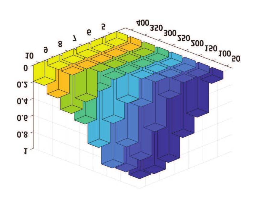
A      PREPRINT   - F EBRUARY 22, 2021

Optical signals of different wavelengths are combined as the matrix B shown in Fig. 1(b) in time domain, by passing
through the MUX. The output intensity IOM 2 U (t) of the OM2 U with the time delay τc ′ is
                                                             N X
                                                             X N
                                         IOM 2 U (t) =                 IA′ (t − τc′ ) · wi,j                                            (4)
                                                             i=1 j=1

Which is equal to the MMAC operation between the flattened convolution kernel vector w′ and the matrix
[A′T , ..., A′T ]which contains N 2 copies of A′ . As depicted in Fig. 1(b), to complete the 2Dconv operation between
A and w, the corresponding elements in (1) should be in the same column of the matrix B′ , which can be realized
by introducing different time delay τ(i−1)×N +j for wavelength λ(i−1)×N +j in TDU to complete the zero padding
operation:

                                      τ(i−1)×N +j = [(N − i) × M ) + N − j]/BR                                                          (5)
The intensity of the light wave passing through the TDU with the wavelength independent circuit time delay                      τc′′   can
be written as
                                               XN X N
                                   ITDU (t ) =        IA′ (t − τc′′ − τ(i−1)×N +j )                                                     (6)
                                                   i=1 j=1

When optical signal is received by the photo-detector (PD), the IT DU (t) convert to VP D (t). Refer to (6), there are
M 2 + (N − 1) × (M + 1) elements in each row of matrix B′ , and the q th column of which occupies one time slice in
VP D (t): from τc′′ + (q − 1)/BR to τc′′ + q/BR, compare the (1) and (6), when
                                     q = (M − N + 1) × (m − 1) + (M + m) + n                                                            (7)
Where 1 ≤ m, n ≤ M − N + 1, and set a parameter σ between 0 and 1, we have:
                                          Ym,n = VP D [(t − τc′′ − q + σ)/BR]                                                           (8)
When M = 3, N = 2 shown in Fig. 1(b), the sum of                 B′i,5 ,
                                                                    Bi,6′ ,     B′i,8 ,
                                                                                  and          B′i,9
                                                                                         corresponding to Y1,1 , Y1,2 , Y2,1 ,
and Y2,2 , respectively. A programmed sampling function refer to (7) and (8) is necessary in digital signal process-
ing, and the parameter σ decides the position of optimal sampling point, which needs to be adjusted at different bit
rates. According to the (5), the row B′q of matrix B′ can be divided into N groups with N vectors composed as a
matrix of Groupi,j = B′(i−1)×N+j , where i, j ≤ N . The kernel elements multiplied with vector A′ in Groupi are
[wi,1 , wi,2 , ..., wi,N ], which are the elements in the same row of a convolution kernel w. Refer to (5), the difference of
the time delay in between two adjacent rows in the same group is equal to 1/BR, whereas the difference of time delay
between Groupi,j and Groupi+1,j is equal to M/BR. The sum of q th column in the same group of B′ can be written
as
                                              X                  XN
                                                   Groupi (q) =      wi,j · A′q+j−N                                       (9)
                                                                   j=1

which is actually the expression of the cross-correlation (marked as R(x, y)) between vector [wi,1 , wi,2 , ..., wi,N ] and
A′ . Therefore, the 2Dconv operation can be decomposed as the sum of multiple double correlation operation between
vectors as follows

                                           2
                                        N
                                        X              N
                                                       X
                                               B′p =         R[R(A′ , wi ), Flatten(Ci )]                                              (10)
                                        p=1            i=1
        PN
where i=1 Ci is an identity matrix with the size of N × N , and the elements at the ith row and column of Ci is equal
to 1, the other elements equal to 0. The matrix Ci is flattened in to a 1 × N 2 vector, and cross-correlation operation is
denoted as R(A′ , wi ).

2.2 The mapping of weight elements to voltage

The MRRs based on electro-optic or thermal-optic effect are used in weighting Bank of OCU. Refer to (3), the elements
of convolution kernel wi,j , trained by 64-bit computer, are usually normalized from 0 to 1, which needs to be mapped
into the transmission of MRRs. As shown in Fig. 2(a), according to [25, 26], the transmission of the through port of

                                                                  3
A PREPRINT - F EBRUARY 22, 2021
MRR based on electro-optic effect is tuned by voltage bias V loaded on the electrode of MRR, which can be written
as:
(1 − α2 )(1 − τ 2 )
T =1− , θ = θ0 + πV /Vπ (11)
(1 − ατ )2 + 4ατ sin2 (θ/2)
Where τ is the amplitude transmission constant between the ring and the waveguide, α is the round-trip loss factor,
and θ is the round-trip phase shift, θ0 is the bias phase of the MRR, and Vπ is the voltage loaded on the MRR when
θ = π , which is decided by the physical parameters of the waveguide. The curve of V-T is shown in Fig. 2(c). A
voltage source with specific precision (10-bit in our evaluation) sweeps the output voltage with the minimum step from
0 to 0.4, which is loaded on the MRR. The transmission metrics of MRR at different voltages are recorded accordingly.
As shown in Fig. 2(d), the processing actually equivalent to sampling the curve of V-T by using an analog-to-digital
converter (ADC) with same precision of the voltage source. If |wi,j | ≤ 1, wi,j can be mapped directly into T , the
weighting voltage V can be figured out by searching the number which is closest to wi,j in the database T-V. Otherwise,
the whole convolution kernel should be normalized through being divided by the max of wi,j . Then, the normalized
wnor matrix is utilized to control signal matrix V. Another mapping method is designed by using part of quasi-linear
region in V-T curve of MRR, where the matrix w needs to be normalized by multiplying max(Tlinear )/max(w). Note
that the error weighting error occurs during the mapping process as shown in Fig. 2(d). There will be a difference w′
between the actual transmission of MRR T ′ and an ideal mapping point T . So the weighting error and outcome of the
OM2 U, Y′ can be written as (12), where Y is the theoretical outcome of the OM2 U, and Y′ → Y when w′ → 0.
w ′ = T′ − T
Weighting Error = [A′T , ..., A′T ] × w′
(12)
Y = [A′T , ..., A′T ] × (w + w′ )
Y′ = Y + Weighting Error
2.3 Dispersed Time Delay Unit
The zero padding operation is executed by offering different time delay for each channel of multi-wavelength light
source in time delay unit. In our previous work [24], the OM2 U based on wavelength division weighting method with
single dispersion compensating fiber (DCF) was proposed, where the correlation operation between two vectors is
realized in time domain refer to (9.) Based on the OM2 U in [24], the TDU can be implemented with single dispersion
media combined with programmed multi-wavelength light source (PMWS) shown in Fig. 3, which can be generated
by a shaped optical frequency comb refer to (5). The programmed light source contains N groups wavelengths, and N
wavelengths are included in each group with the wavelength spacing of ∆λ, the wavelength spacing between adjacent
groups is equal to M × ∆λ. The requirements of programmed multi-wavelength light source can be written as
P M W Si,j − P M W Si,j−1 = ∆λ
(13)
P M W Si,j − P M W Si−1,j = M × ∆λ
where P M W S is programmable multiple-wavelength source, which is sent to the dispersion media with length of L
(km), and the dispersion of D (s/nm/km). Therefore, the time delay difference marked as TDD in 14) are introduced
for optical signal with wavelength P M W Si,j to the P M W S1,1 . This value is equal to
T DDi,j = (P M W Si,j − P M W S1,1 ) × LD (14)
When T DDi,j − T DDi,j−1 = 1/BR, (14) is equivalent to (5), i.e. zero padding operation is conducted when multi-
wavelength signals passing through the dispersion media. Note that there exist challenging tasks in implementing the
TDU structure as shown in Fig. 3. It is essential to design the frequency comb with large enough number and density
of lines combine with dispersion media with flat, large enough D (s/nm/km) and low loss. The bandwidth, B with the
number of lines, k, and the length of DCF, L needed can be calculated as:
B = (M + 1) × (N − 1) × ∆λ
k = B/∆λ + 1 (15)
L = (BR × D × ∆λ)−1
In this paper we take frequency comb with ∆λ ≈ 0.2 nm as reported in [27] and DCF (suppose D is flat for all
wavelength) with D = −150 (ps/nm/km), to perform MNIST handwritten digit recognition task, where M = 28,
N = 3 for example, refer to (15) with B = 11.6 nm, k = 59 lines, and L = 1.67 km at BR = 20 G.
4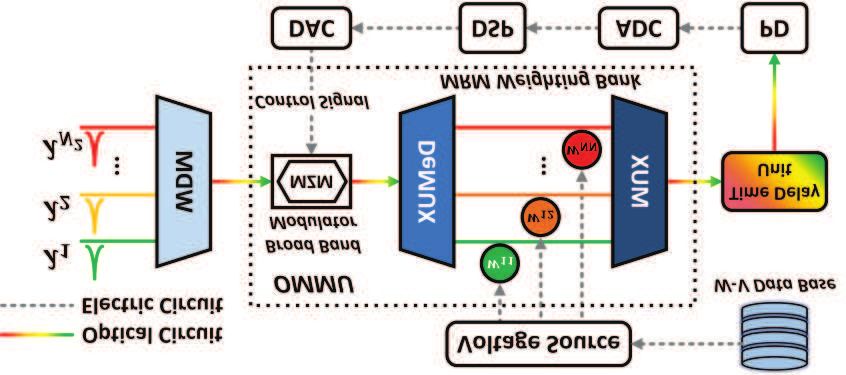
A   PREPRINT   - F EBRUARY 22, 2021

Another widely discussed structure of dispersed delay architecture is based on multi-wavelength source and arrayed
fiber grating, where the PMWS is not necessary, and the cost of source and bandwidth is much cheaper. However, at
least N 2 SMF are needed, which makes it hard to control the time delay of each wavelength precisely. N 2 tunable
time delay units for short time delay such as Fiber Bragg Grating and Si3 N4 waveguide can be employed with proper
delay controller to compensate the time delay error in each channel caused by fabrication process. Furthermore, the
size of input images Ml for the lth convolution layer is equal to half of Ml−1 after pooling operation with stride of 2,
the length of SMF for lth convolution layer need to be adjusted according to Ml , whereas the TDU based on PMWS
and single DM can regulate the time delay with high robustness by reprogramming WDM source according to (14).

3    Photonic CNN Architecture

As shown in Fig. 4(a), a simplified AlexNet convolution neural network for MNIST handwritten digit recognition task
is trained offline on 64-bit computer in TensorFlow framework (TCNN), which is composed of 3 convolution layers,
and 2 kernels (3 × 3 × 1), 4 kernels (3 × 3 × 2) and 4 kernels (3 × 3 × 4) in the 1st , 2nd and 3th convolution
layer, respectively. The size of samples in MNIST written digital dataset 28 × 28 × 1 (W idth × Height × Channel),
and the output shape for each layer is (13 × 13 × 2), (5 × 5 × 4), (3 × 3 × 4), and finally a (1 × 36) flatten feature
vector (marked as FFV in equations) is output by the flatten layer. A PCNN simulator with the same architecture
is set up based on Lumerical and Matlab to implement the optical domain and DSP part of the OCU. The V − T
database is established by recording the transmission of corresponding wavelength at through port of the default MRR
offered by lumerical, while sweeping voltage bias from 0 to 1.2 V with precision of 10-bit. Then the mapping process
shown in Fig. 2 is conducted to load convolution kernel into the PCNN simulator. The feature map extracted at each
convolution layer of input figure “8” from TensorFlow and reshaped feature vector of PCNN are compared in Fig.
4(b), which shows the feature map extraction ability of the PCNN. Finally 200 test samples in MNIST are extracted
randomly and sent to the PCNN for test with the test accuracy is 85% at 10 G Baud Rate. Note that the TensorFlow is
a simplified AlexNet whose classification accuracy for the same 200 test samples is only 86.5% in our 64-bit computer.
The confusion matrices of TensorFlow and PCNN at 10G Baud Rate are shown in Fig. 5 (a) and (b), respectively.

4 Evaluation of Photonic CNN

4.1 Weighting Error of MRR Weighting Bank

Equation (12) shows that the weighting error occurs during mapping process, which is depending on the mapping
precision P (vi ) of the MRR weigting bank. The P (vi ) can be evaluated by the difference of the T (vi ) [20], which is

                                P (vi ) = log2 [∇T (vi )]−1 = log2 [T (vi ) − T (vi−1 )]−1                           (16)

As shown in Fig. 6, we numerical analyze the P (vi ) of MRR with different fineness at distinct ADC precision
level refer to (11) and (16). In Fig. 6(b), the MRR with smaller fineness has higher P (vi ) in quasi-linear region
(vi ≤ vl , where vl is the boundary of quasi-linear region ). However, when vi ≥ vl , P (vi ) increases with the fineness.
The precision of ADC also has impact on the P (vi ) of MRR. As depicted in Fig. 6 (c), P (vi ) increases with the
precision of ADC. The weighting error separated from the PCNN is added to the flatten feature vector extracted from
the TensorFlow CNN. The test accuracy of flatten feature vector is 87%, with the confusion matrix shown in Fig. 5
(c). Note that the test accuracy of flatten feature vector with error is higher than that in TensorFlow, the handwritten
digital recognition task in this paper is a 36-dimensions optimal task. Here we use 1-dimension optimal function g(x)
to explain. As shown in Fig. 6(d), there is a distance D between the optimal point and the convergence point of
TensorFlow. The convergence point of PCNN can be treated as optimal point of TCNN added with noises in error
range. This deviation will probably lead to a closer location to the optimal point and therefore a higher test accuracy
with a certain probability. The test accuracy of MRR with different fineness at distinct ADC precision level is shown
in Fig. 6(e), where the wi,j is mapped into T from 0 to 1, whereas wi,j is mapped into T in quasi-linear region in Fig.
6(f). By comparing two figures, the MRR with low fineness and high ADC precision level are preferred in high-speed
photonic CNN.

                                                            5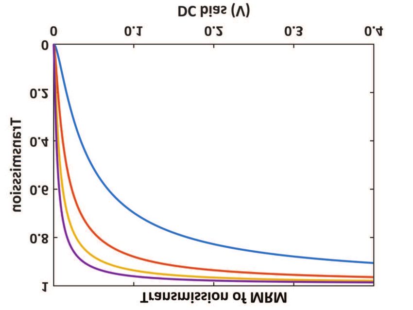
A PREPRINT - F EBRUARY 22, 2021
Table 1: EXECUTION SPEED AT DIFFERENT BAUD RATE FOR PCNN WITH 1 OCU
Time of Conv.1 Time of Conv.2 Time of Conv.3
Baud Total Execution Speed Execution Speed
(M=28) (M=13) (M=5) Ops
Rate time (Average) (2Dconv)
Period =2 Period =8 Period=16
5G 340 ns 320 ns 128 ns 788 ns 56 GOPS 71 GOPS
10G 170 ns 160 ns 64 ns 394 ns 112 GOPS 143 GOPS
15G 114 ns 112 ns 40 ns 266 ns 44352 166 GOPS 213 GOPS
20G 86 ns 80 ns 32 ns 198 ns 224 GOPS 282 GOPS
25G 68 ns 64 ns 24 ns 156 ns 284 GOPS 357 GOPS
4.2 Computation Speed
The distortion will be introduced when high bandwidth signals passing through filters such as MRR. Moreover, the
quantization noise for high frequency signals will also induce the extra error, which can be extracted refer to (17):
Error = FFVPCNN − FFVTCNN − Weighting Error (17)
where Weighting Error is fixed at any baud rate in our simulator. We run the photonic CNN at the baud rate of 5,
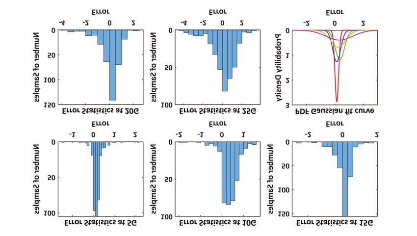
10, 15, 20, and 25 Gbaud for 10 samples. The distribution statistics of Error with 360 elements at each baud rate is
shown are Fig. 7 (a) to (e). To analyze the impact of levels of error on the test accuracy at different baud rates, the
probability density function (PDF) of the error at each baud rate are calculated. The PDF shows a normal distribution,
and the Gaussian fit curve of PDF at each baud rate is shown in Fig. 7(f). The mean value of Gaussian fit function
will decrease whereas variance increases at higher baud rate for input vector, meaning that the error will increase with
the baud rate. 10 random error sequences Error′i are generated according to the PDF at each baud rate and added with
(FFVT CN N + Weighting Error), which are combined as new flatten feature vector with errors sent to the classifier
for testing. The performance of photonic CNN at different baud rate is shown in Fig. 8. Note that the distance between
the optimal point and the convergence point is shown in Fig. 6(d). The difference of average accuracy at each baud
rate and standard deviation of test accuracy should be considered instead. In Fig. 8, the performance degrades with the
increasing of baud rate, showing that the high speed photonic CNN will pay its the cost of computation performance.
However, high operation baud rate will mean less computing time, which can be roughly calculated as
t2Dconv = [M × (M + 2) + 2]/BR + tc (18)
Table 2: EXECUTION SPEED AT DIFFERENT BAUD RATE FOR 4 × 4 PCNN MESH
Baud Time of Conv.1 Time of Conv.2 Time of Conv.3 Total Execution Speed Execution Speed
Ops
Rate (M=28) (M=13) (M=5) time (54% Utilization) (100% Utilization)
5G 170 ns 40 ns 8 ns 218 ns 203 GOPS 324 GOPS
10G 85 ns 20 ns 4 ns 109 ns 406 GOPS 648 GOPS
15G 57 ns 14 ns 2.5 ns 73.5 ns 44352 603 GOPS 1.03 TOPS
20G 43 ns 10 ns 2 ns 55 ns 806 GOPS 1.29 TOPS
25G 34 ns 8 ns 1.5 ns 43.5 ns 1.02 TOPS 1.73 TOPS
Where tc is the time delay in OM2 U, which is usually less than 100 ps in our system. Thus, the execution speed at
different are as shown in Table 1. Note that the operation in TCNN is a 4-dimension operation (or tensor operation) for
width, height, channel and kernel. However, for each OCU only 2-dimension operation for width, height is realized
during one period. In the layer of a photonic CNN with input of C channels and K kernels, one OCU can be used
repeatedly to complete 4-dimension operation in C × K periods. To improve the execution speed, the parallelization
of the photonic CNN is necessary in the future. In this paper, a candidate mesh with MRR weighting bank shown in
Fig. 9 is proposed to complete tensor operation during one period. Each row of the mesh is combined as one kernel
with all channels. And the same channel of input figure is copied and sent to the mesh in the same column. For the
first layer of photonic CNN, the input image “8” is flattened into 1 × 784 vector and duplicated into two copies by a
splitter for M W B1,1 and M W B2,1 . Two 1 × 842 vectors are sent to the DSP through the TDU and PD in the 1st
and 2nd row of mesh. Note that the length of optical path through mesh and dispersion media should be equal. The
6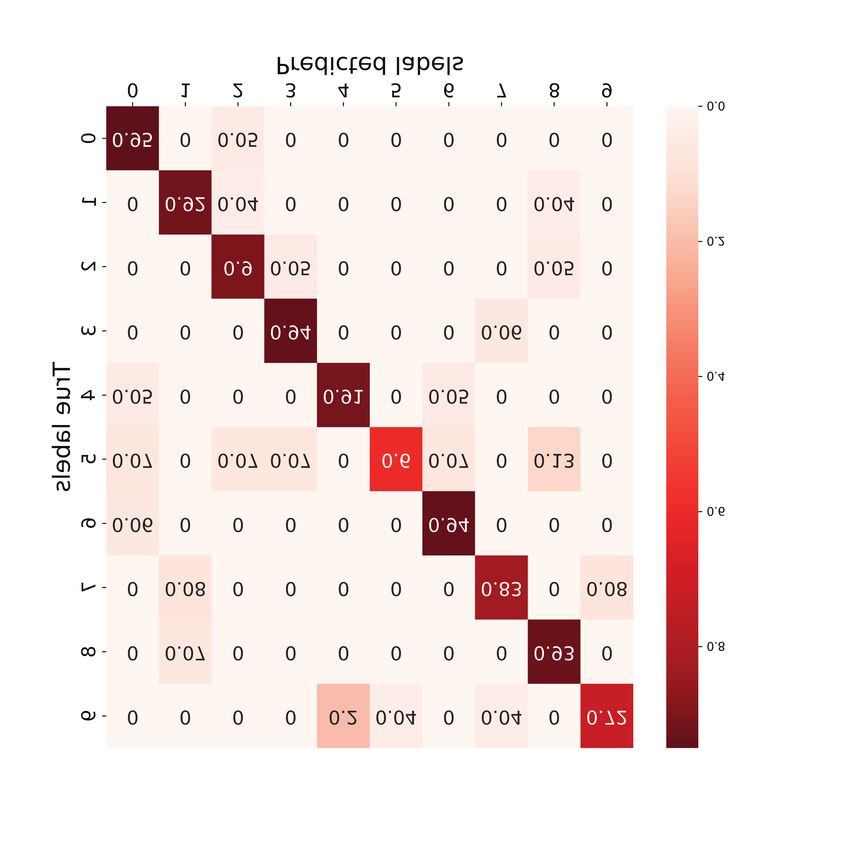
A   PREPRINT   - F EBRUARY 22, 2021

execution speed of the 4×4 mesh at different baud rate is shown in Table. 2. Note that the mesh is not 100% utilized in
each period when loaded a simplified AlexNet shown in Fig. 4(a). The average utilization of PCNN can be calculated
as 2/16 + 8/16 + 16/16 = 54%, thus the average execution time for one sample is much lower due to nature of
parallelization. Refer to (15) and Table 1, and 2, the photonic CNN running at higher baud rate has faster execution
speed and lower delay scale. However, the selection of baud rate depends on the requirement of CNN performance and
time delay resolution. As shown in Fig. 8, the performance degenerate significantly at Baud Rate = 25 G. Moreover,
if we choose the delay structure in Fig. 3, and we set the length of DCF of L = 2km and comb with density of 0.2
nm, R = 60 ps according to (15), which allows Baud Rate ≤ 16.7 G.

4.3 Memory Cost

The photonic CNN using electronic buffer based on 2Dconv and GeMM algorithm need to access to memory reapeatly
to extract the corresponding image slice. The number of times for memory access is 2 × (M − N + 1)2 . As shown in
Fig. 10(a), memory access times for 2Dconv and GeMM algorithm will increase significantly with the width of input
image, since that multiplication, addition and zero padding operations will require a large amount of data in memory
shown in Fig. 10(b). However, photonic CNN only needs to take out the flatten image vector and store the convolution
results, i.e. only 2 times for memory access are needed. Further more, intermediate data stored in the optical delay
unit which will have less memory cost compared to electrical counterpart as in Fig. 10 and very close to the theoretical
lower limit.

5 Conclusion
In this paper, we propose a novel integrated photonic CNN based on double correlation operations through interleaved
timewavelength modulation. 200 images are tested in MNIST datasets with accuracy of 85.5% in our PCNN versus
86.5% in 64-bit computer. The error caused by distortion induced by filters and ADC will increases with the baud rate
of the input images, leading to the degradation of classification performance. A tensor processing unit based on 4 × 4
mesh with 1.2 TOPS (operation per second when 100% utilization) computing capability at 20G baud rate is proposed
and analyzed to form a paralleled photonic CNN.

References
 [1] Yann LeCun, Yoshua Bengio, and Geoffrey Hinton. Deep learning. nature, 521(7553):436–444, 2015.
 [2] Alex Krizhevsky, Ilya Sutskever, and Geoffrey E Hinton. Imagenet classification with deep convolutional neural
     networks. In Advances in neural information processing systems, pages 1097–1105, 2012.
 [3] Karen Simonyan and Andrew Zisserman. Very deep convolutional networks for large-scale image recognition.
     arXiv preprint arXiv:1409.1556, 2014.
 [4] Christian Szegedy, Wei Liu, Yangqing Jia, Pierre Sermanet, Scott Reed, Dragomir Anguelov, Dumitru Erhan,
     Vincent Vanhoucke, and Andrew Rabinovich. Going deeper with convolutions. 2014.
 [5] Yangqing Jia. Learning semantic image representations at a large scale. 2014.
 [6] Kaiming He and Jian Sun. Convolutional neural networks at constrained time cost. In 2015 IEEE Conference on
     Computer Vision and Pattern Recognition (CVPR), 2015.
 [7] Marat Dukhan. The indirect convolution algorithm. 2019.
 [8] Zhi-Gang Liu, Paul N Whatmough, and Matthew Mattina. Systolic tensor array: An efficient structured-sparse
     gemm accelerator for mobile cnn inference. IEEE Computer Architecture Letters, 19(1):34–37, 2020.
 [9] Andrew Lavin and Scott Gray. Fast algorithms for convolutional neural networks. 2015.
[10] Minsik Cho and Daniel Brand. Mec: memory-efficient convolution for deep neural network. arXiv preprint
     arXiv:1706.06873, 2017.
[11] Tao Luo, Shaoli Liu, Ling Li, Yuqing Wang, and Yunji Chen. Dadiannao: A neural network supercomputer.
     IEEE Transactions on Computers, 66(1):73–88, 2016.
[12] Shunsuke Suita, Takahiro Nishimura, Hiroki Tokura, Koji Nakano, Yasuaki Ito, Akihiko Kasagi, and Tsuguchika
     Tabaru. Efficient cudnn-compatible convolution-pooling on the gpu. In International Conference on Parallel
     Processing and Applied Mathematics, pages 46–58. Springer, 2019.
[13] Shunsuke Suita, Takahiro Nishimura, Hiroki Tokura, Koji Nakano, and Tsuguchika Tabaru. Efficient convolution
     pooling on the gpu. Journal of Parallel and Distributed Computing, 138:222–229, 2020.

                                                           7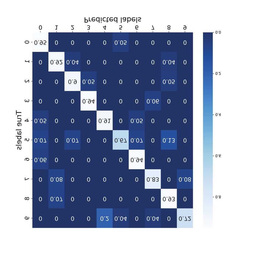
A   PREPRINT   - F EBRUARY 22, 2021

[14] Norman P Jouppi, Cliff Young, Nishant Patil, David Patterson, Gaurav Agrawal, Raminder Bajwa, Sarah Bates,
     Suresh Bhatia, Nan Boden, Al Borchers, et al. In-datacenter performance analysis of a tensor processing unit. In
     Proceedings of the 44th Annual International Symposium on Computer Architecture, pages 1–12, 2017.
[15] Yu Wang. Neural networks on chip: From cmos accelerators to in-memory-computing. In 2018 31st IEEE
     International System-on-Chip Conference (SOCC), pages 1–3. IEEE, 2018.
[16] H John Caulfield and Shlomi Dolev. Why future supercomputing requires optics. Nature Photonics, 4(5):261–
     263, 2010.
[17] Yichen Shen, Nicholas C Harris, Scott Skirlo, Mihika Prabhu, Tom Baehr-Jones, Michael Hochberg, Xin Sun,
     Shijie Zhao, Hugo Larochelle, Dirk Englund, et al. Deep learning with coherent nanophotonic circuits. Nature
     Photonics, 11(7):441, 2017.
[18] Philip Y Ma, Alexander N Tait, Thomas Ferreira de Lima, Chaoran Huang, Bhavin J Shastri, and Paul R Prucnal.
     Photonic independent component analysis using an on-chip microring weight bank. Optics Express, 28(2):1827–
     1844, 2020.
[19] Alexander N Tait, Hasitha Jayatilleka, Thomas Ferreira De Lima, Philip Y Ma, Mitchell A Nahmias, Bhavin J
     Shastri, Sudip Shekhar, Lukas Chrostowski, and Paul R Prucnal. Feedback control for microring weight banks.
     Optics express, 26(20):26422–26443, 2018.
[20] Qixiang Cheng, Jihye Kwon, Madeleine Glick, Meisam Bahadori, Luca P Carloni, and Keren Bergman. Silicon
     photonics codesign for deep learning. Proceedings of the IEEE, 2020.
[21] Armin Mehrabian, Mario Miscuglio, Yousra Alkabani, Volker J Sorger, and Tarek El-Ghazawi. A winograd-
     based integrated photonics accelerator for convolutional neural networks. IEEE Journal of Selected Topics in
     Quantum Electronics, 26(1):1–12, 2019.
[22] Hengameh Bagherian, Scott Skirlo, Yichen Shen, Huaiyu Meng, Vladimir Ceperic, and Marin Soljacic. On-chip
     optical convolutional neural networks. arXiv preprint arXiv:1808.03303, 2018.
[23] Shaofu Xu, Jing Wang, and Weiwen Zou. Optical patching scheme for optical convolutional neural networks
     based on wavelength-division multiplexing and optical delay lines. Optics Letters, 45(13):3689–3692, 2020.
[24] Yuyao Huang, Wenjia Zhang, Fan Yang, Jiangbing Du, and Zuyuan He. Programmable matrix operation with
     reconfigurable time-wavelength plane manipulation and dispersed time delay. Optics express, 27(15):20456–
     20467, 2019.
[25] Hidehisa Tazawa, Ying-Hao Kuo, Ilya Dunayevskiy, Jingdong Luo, Alex K-Y Jen, Harold R Fetterman, and
     William H Steier. Ring resonator-based electrooptic polymer traveling-wave modulator. Journal of lightwave
     technology, 24(9):3514, 2006.
[26] Bartosz Bortnik, Yu-Chueh Hung, Hidehisa Tazawa, Byoung-Joon Seo, Jingdong Luo, Alex K-Y Jen, William H
     Steier, and Harold R Fetterman. Electrooptic polymer ring resonator modulation up to 165 ghz. IEEE Journal of
     Selected Topics in Quantum Electronics, 13(1):104–110, 2007.
[27] Junqiu Liu, Erwan Lucas, Arslan S. Raja, Jijun He, and Tobias J. Kippenberg. Author correction: Photonic
     microwave generation in the x- and k-band using integrated soliton microcombs. Nature Photonics, pages 1–1,
     2020.

                                                         8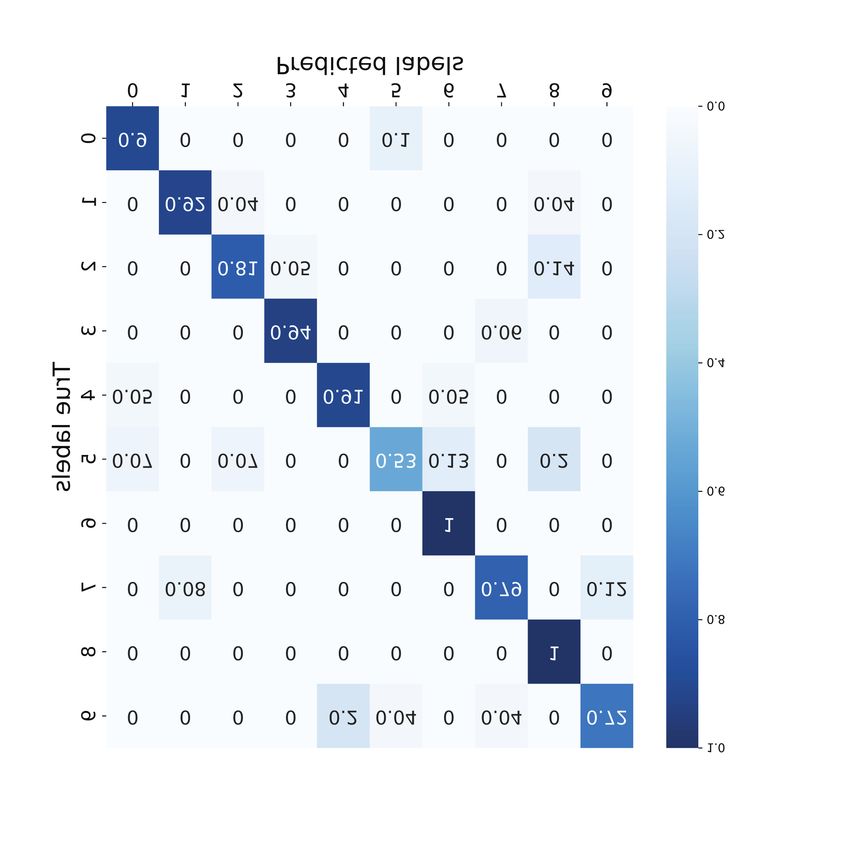
A   PREPRINT   - F EBRUARY 22, 2021

         Image: M×M

                                 Flatten

                          Flatten

                   Convolution
                   Kernel: N×N                                  Zero Padding

       Feature Map:
     (M-N+1)×(M-N+1)
       For: M=3,N=2

Figure 1: (a) Structure of the OCU, where the 2Dconv operation shown in (b) is done. MZM: Mach Zehnder modulator,
W-V Data Base: set up following the process shown in Fig. 2(b) to generate the voltage control signal loaded on
the MRR weigthting bank, PD: Photodetector to covert optical signal into electric domain, ADC and DAC: Analog-
to-Digital and Digital-to-Converter respectively, DSP: Digital signal processing where the sampling, nonlinear, and
pooling operation is done.

                                                        9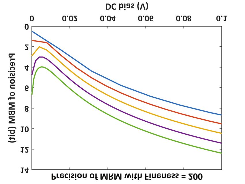
A    PREPRINT    - F EBRUARY 22, 2021

                                                                                                  MRM            64-bit Computer

    (a)                                                   V             (b)
                                                                                                                                     v-T Curve

                                                                                                                     Training

                                                                                               Control Signal        W Data             ADC
                                                                                                                      Base
                                                                                                Mapping
                  in                                   Through                                  Fuctions
                                                                                                                                     Sampled
                                                                                                                    V-T Data
                                                                                                                                     v-T Curve
                                                                                                                      Base

                   - Curve and                      Curve of MRM                                    Sampled - Curve of MRM
    (c)                                                                 (d)
   Transmission

                                                                        Transmission
                                 QLR
                                                                                                                 Mapping        Weighting Error

                                       Voltage                                                                    Voltage

Figure 2: (a) Schematic of MRR based on EO effect, (b) Mapping process of w to T − V . (c) v − T and ∇T (v)
curve of MRR, the QLR (quasi-linear region) in this paper is defined as the region between 0 v and the corresponding
voltage at the highest 1/3 of the ∇T (v) curve , (d) v − T curve sampled by ADC with 10-bit precision, note that there
are error w′ existed between theoretical mapping points wi,j and true mapping points Ti,j
                                                                                       ′
                                                                                          .

                                                           Dispersion
                                       PD                   Medium

                                                                                                      WSBG

                                                               Wave
                                                                                       Power
                       Power

                                                              Shaper

                                       Wavelength                                                            Wavelength
                               WDM Generated from OFC                                    Programed Multi-Wavelength Source

Figure 3: TDU based on single dispersion medium and Programmed multi-wavelength source, which is generated by
the optical comb and wave shaper, with N groups wavelengths, and N wavelengths in each group, with the wavelength
distance of ∆λ, and the wavelength space between adjacent groups marked as W SBG = ∆λ · M .

                                                                   10
A PREPRINT - F EBRUARY 22, 2021
Input Image ć8Ĉ Input Image ć8Ĉ
(a) (b)
Electric
Domain
28×28×1 28×28×1
Conv.1 (2 kernels, 3×3×1) Flatten
2×1×784
Relu
Conv.1 (2 OCUs)
Optical
Max Pooling OCU.1 OCU.2
13×13×2
Domain
Conv.2 (4 kernels,3×3×2) 2×1×842
Sampling
Relu
Electric
Bias and Relu
Max Pooling Domain
5×5×4
Conv.3 (4 kernels,3×3×2) Max Pooling
DSP
Relu
4×2×169
Conv.2 (8 OCUs)
Max Pooling
3×3×4 4×4×25
Flatten Conv.3 (16 OCUs)
1×36 1×36
TCNN PCNN Feature Map of TCNN Feature Map of PCNN
Figure 4: (a)The architecture of convolutional neural network in TensorFlow (TCNN) with 3 convolution layers and
the PCNN with the same architecture of TCNN, (b) Compare of feature map extracted by TCNN and reshaped feature
vector extracted by PCNN.
Confusion Matrix of TCNN Confusion Matrix of PCNN at 10G Baud Rate Confusion Matrix of TCNN with Weighting Error
(a) (b) (c)
Figure 5: (a) Confusion matrix of TCNN for 200 samples test, (b) Confusion matrix of PCNN at 10G Baud Rate, (c)
Confusion matrix of TCNN with weighting bank error separated from PCNN.
11A PREPRINT - F EBRUARY 22, 2021
Fineness = 100 Fineness = 100
Fineness = 150 Fineness = 150
Fineness = 200 Fineness = 200
Fineness = 250 Fineness = 250
(a) (b)
Optimal Point
Convergence Point
PCNN Point
Error Range
6bit ADC
7bit ADC
8bit ADC D
9bit ADC
10bit ADC
(c) (d)
Test Accuracy
Test Accuracy
(e) (f)
Figure 6: (a) T − V curve of MRR with different Fineness from 100 to 250, (b) Compare of weighting precision of
MRR with different Fineness, (c) Compare of weighting precision of the MRR at different level of ADC precision, (d)
The PCNN point which is equal to Convergence Point of TCNN with error may have shorter distance to the optimal
point compared with that of TCNN, which leads to higher test accuracy, (e) Test Accuracy compare of MRR with
different Fineness at distinct ADC precision level when wi,j is mapped into T from 0 to 1, whereas (f) wi,j is mapped
into T in quasi-linear region.
12A PREPRINT - F EBRUARY 22, 2021
(a) (b) (c)
(d) (e) (f)
5G
10G
15G
20G
25G
Figure 7: (a) to (e), the distribution statistics of Error at the Baud Rate of 5,10,15,20, and 25G, respectively, (f) The
Gaussian fit curve of probability density function (PDF) of Error at different Baud Rate.
Figure 8: Performance of PCNN at different Baud Rate, the standard deviation is adopted here, note that, Error of
TCNN and TCNN with Weighting Error (WE) are equal to 0, i.e. the std at TCNN and Weighting Error are 0.
13A PREPRINT - F EBRUARY 22, 2021
WDM
DeMUX
MZM
MZM
MZM
MZM
MUX
...
MRR Weighting Bank
11 21 21 21
TDU PD
12 22 22 22
TDU PD
13 23 23 23 DSP
TDU PD
14 24 24 24
TDU PD
Figure 9: PCNN based on C × K MWB (MRR weighting bank) mesh, the MWB in each column are for the same
input channel in different kernels, and the MWB in each row combine as one kernel with C channels.
TMA of 2Dconv and GeMM Compare of Memory Cost
Memory Cost (Elements)
Times of Memory Access
(a) (b)
Theoretical limit
PCNN in our work
PCNN with Electric Buffer
Width of Image (Square) Width of Image (Square)
Figure 10: (a) Times of Memory Access (TMA) of 2Dconv, GeMM algorithms and the PCNN based on electronic
buffer, where as the memory access of the PCNN based on TDU is fixed and equal to 2, (b) Compare of Memory cost
between PCNN in ourwork, PCNN based on electric buffer and 2Dconv algorithm, which is also the theoretical lower
limit of CNN.
14You can also read