Power Electronics: Ceramic Embedding Gives a Boost to Wide Bandgap Semiconductor Devices - Fraunhofer IISB
←
→
Page content transcription
If your browser does not render page correctly, please read the page content below
Press Release, April 12, 2019

Power Electronics: Ceramic Embedding Gives a Boost to
Wide Bandgap Semiconductor Devices

The use of power electronics in challenging fields of application – such
as electric vehicles or aerospace – implies high requirements
concerning switching speed and reliability. In this context, conventional
packaging technologies are often pushed to thei r limits. Scientists at
Fraunhofer IISB have developed a novel packaging concept and
technologies by embedding power semiconductor devices into ceramic
circuit carriers. Their design offers high temperature stability, operation
at high voltages, and hermet ic sealing to provide maximum lifetime in
harsh environments. This helps to fully exploit the great advantages of
wide-bandgap semiconductors (W BG). Power modules based on this
new approach are presented by Fraunhofer IISB at this year’s PCIM
Europe exhibition in May 2019 in Nuremberg.

    Power module made with the Ceramic Embedding technology. © Fraunhofer IISB
Ongoing miniaturization, 3D integration, and extreme environmental conditions
impose major challenges to future power devices, modules, and systems, which are
expected to provide excellent performance, high reliability, and long lifetime. Low
cost is a key, enabled by high temperature. This implies small chip size and low
cooling effort. In this respect, the applicability of established packaging technologies,
e.g., based on PCBs (Printed Circuit Boards), is limited as they do not afford
sufficient thermal stability or current carrying capability. As a remedy, a novel
packaging concept was developed at Fraunhofer IISB in Erlangen, which is based on
the embedding of power semiconductors in ceramic circuit carriers.
This prepares the ground for an extensive and more economical use of wide-
bandgap semiconductors such as SiC (silicon carbide). SiC devices offer a vast
potential for the growing market of power electronics. They allow the switching of
very high currents and voltages in compact, miniaturized systems and thus are a key
enabler for the development of highly efficient and intelligent solutions for mobility,
industrial applications, and energy technology. With the new approach for packaging
and circuit carriers, the existing physical constraints, such as limited operation
temperature or undesired parasitic inductances, can be enhanced.
With the new technology – called Ceramic Embedding – the power devices are
placed inside a special prepared direct bonded copper (DBC) substrate by suitable
die bonding techniques such as soldering or silver sintering. Subsequently, all gaps
are filled with a high-temperature potting material. The resulting prepackage is
forming an easy-to-use power electronics building block.
The concept allows a high copper layer thickness, which paves the way for a
considerable current carrying capacity. A big benefit is the high electrical and thermal
contact area. The semiconductor’s top and bottom side have ideal interconnections
offering the full performance of the tiny WBG devices.
Different types of ceramic material are applicable such as alumina, aluminum nitride
or silicon nitride. The choice depends on the individual requirements for optimizing
the thermal management, mechanical properties, and cost.
For generating the cavities and trenches, subtractive manufacturing methods are
used. The vias for the electrical contacts are drilled with a laser process. Then they
are filled with silver sintering material or similar conductive materials. The vias allow
the realization of multi-layer ceramic substrate stacks, which are of special
advantage for low-inductance commutation cells.
Fraunhofer IISB is continuing its intensive research on Ceramic Embedding and the
necessary manufacturing process technologies to exploit the full potential of wide-
bandgap semiconductor devices in power electronics. The target is to bring the
promising packaging technology to industrial production.
Power modules based on the Ceramic Embedding technology can be discovered on
May 7-9, 2019, at the PCIM Europe exhibition in Nuremberg, booth no. 6-438.
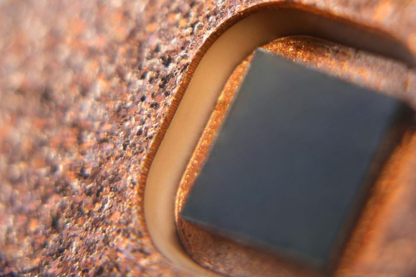
Close-up view of a wide-bandgap device embedded by the Ceramic Embedding technology.
© Fraunhofer IISB
For further information, contact
Andreas Schletz
Fraunhofer IISB, Schottkystrasse 10, 91058 Erlangen, Germany
Tel. +49 9131 761 187 | andreas.schletz@iisb.fraunhofer.de
www.iisb.fraunhofer.deAbout Fraunhofer IISB Founded in 1985, the Fraunhofer Institute for Integrated Systems and Device Technology IISB conducts applied research and development in the fields of power electronics, energy electronics, and semiconductors according to the Fraunhofer model. As a result, the institute comprehensively covers the value-added chain for complex electronics systems, from the basic material to complete electronics and energy systems. Research focuses on the application areas of electromobility and energy supply. For its customers, the institute develops solutions in the fields of material development, semi-conductor technology and manufacturing, electronic components devices and modules, construction packaging and connection technology, simulation, reliability, up to system development in vehicle electronics, energy electronics, and energy infrastructure. Among other things, the IISB has extensive know-how in semiconductor basic material and characterization. The main location of Fraunhofer IISB is in Erlangen, Germany. There are further locations at the Energie Campus Nürnberg (EnCN) in Nuremberg as well as in Freiberg.
You can also read


