Spectral imaging and spectral LIDAR systems: moving toward compact nanophotonics-based sensing - De Gruyter
←
→
Page content transcription
If your browser does not render page correctly, please read the page content below
Nanophotonics 2021; 10(5): 1437–1467

Review

Nanxi Li*, Chong Pei Ho, I-Ting Wang, Prakash Pitchappa, Yuan Hsing Fu, Yao Zhu
and Lennon Yao Ting Lee

Spectral imaging and spectral LIDAR systems:
moving toward compact nanophotonics-based
sensing
https://doi.org/10.1515/nanoph-2020-0625                              1 Introduction
Received November 25, 2020; accepted January 16, 2021;
published online February 12, 2021
                                                                      Optical imaging and sensing systems are key components in
                                                                      industrial automation and consumer electronics. The wide
Abstract: With the emerging trend of big data and
                                                                      distribution of these sensing systems enables data genera-
internet-of-things, sensors with compact size, low cost and
                                                                      tion to meet the emerging global trend of big data and
robust performance are highly desirable. Spectral imaging
                                                                      internet-of-things [1]. In order to sense the spectral infor-
and spectral LIDAR systems enable measurement of spec-
                                                                      mation of the object, spectral imaging technology has been
tral and 3D information of the ambient environment. These
                                                                      developed and widely applied. The spectral imager collects
systems have been widely applied in different areas
                                                                      2-dimensional (2D) images of the object at different wave-
including environmental monitoring, autonomous driving,
                                                                      lengths and forms an imaging stack. Hence, at each pixel,
biomedical imaging, biometric identification, archaeology
                                                                      there is a data cube containing the spectral information of
and art conservation. In this review, modern applications
                                                                      the object corresponding to the selected pixel location. From
of state-of-the-art spectral imaging and spectral LIDAR
                                                                      this spectral information, the material or chemical compo-
systems in the past decade have been summarized and
                                                                      sition of the object can be determined. Depending on the
presented. Furthermore, the progress in the development
                                                                      number of spectral bands within the stack or data cube,
of compact spectral imaging and LIDAR sensing systems
                                                                      spectral imaging can be subcategorized into multispectral
has also been reviewed. These systems are based on the
                                                                      and hyperspectral imaging, which typically contains 3–10
nanophotonics technology. The most updated research
                                                                      bands and dozens to hundreds of bands, respectively [2].
works on subwavelength scale nanostructure-based func-
tional devices for spectral imaging and optical frequency             The spectral imaging technology, which is able to obtain
comb-based LIDAR sensing works have been reviewed.                    both spatial and spectral information, was originally
These compact systems will drive the translation of spectral          applied in Earth remote sensing [3]. Currently, it has been
imaging and LIDAR sensing from table-top toward portable              widely utilized in remote and indoor sensing, covering from
solutions for consumer electronics applications. In addi-             Earth observation, geo-information study [4–7] to optical
tion, the future perspectives on nanophotonics-based                  sorting and pharmaceutical analysis [8, 9].
spectral imaging and LIDAR sensing are also presented.                     In addition to spectral information, to sense the
                                                                      3-dimensional (3D) information of the object, light detec-
Keywords: LIDAR; nanophotonics; sensor; spectral imaging.             tion and ranging (LIDAR) technology provides an effective
                                                                      solution. LIDAR system primarily consists of a light source
                                                                      and a detector. By tracking the reflected signal from the
                                                                      object in ambient environment, the location and velocity
*Corresponding author: Nanxi Li, Institute of Microelectronics,
A*STAR (Agency for Science, Technology and Research),                 information of the object can be obtained. The location
2 Fusionopolis Way, Singapore 138634, Singapore,                      information can then be used to reconstruct the 3D image
E-mail: linx1@ime.a-star.edu.sg. https://orcid.org/0000-0002-0524-    of the object. LIDAR technology has been widely used in
0949                                                                  advanced driver-assistance systems (ADAS), autonomous
Chong Pei Ho, I-Ting Wang, Prakash Pitchappa, Yuan Hsing Fu, Yao
                                                                      driving and 3D sensing. It has become the eyes of robotics
Zhu and Lennon Yao Ting Lee, Institute of Microelectronics, A*STAR
(Agency for Science, Technology and Research), 2 Fusionopolis Way,
                                                                      and cars to sense the ambient environment. The LIDAR
Singapore 138634, Singapore. https://orcid.org/0000-0002-7691-        technology has also been combined with the aforemen-
0196 (Y.H. Fu)                                                        tioned spectral imaging technology to realize spectral
  Open Access. © 2021 Nanxi Li et al., published by De Gruyter.   This work is licensed under the Creative Commons Attribution 4.0 International
License.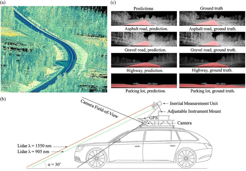
1438          N. Li et al.: Spectral imaging and spectral LIDAR systems

LIDAR sensing systems [10–13]. It can be used to determine                applications have been reported before [2, 22, 25, 30–32].
the shape as well as the material composition of the ob-                  However, the progress report on nanophotonics-based
jects, as different materials have unique reflectance in the               spectral imaging and LIDAR sensing systems is lacking. In
optical spectrum. For example, the spectral reflectance of                 this review, we summarized the recent research works on
various plant species [14], gravel grain sizes [15], asphalt              spectral imaging and spectral LIDAR systems, including the
surfaces [16] are different and hence can be distinguished                nanophotonics-based sensing systems. The modern appli-
by using a multispectral imaging system.                                  cations of the current state-of-the-art spectral imaging and
     Modern applications of spectral imaging and spectral                 spectral LIDAR systems are presented in Section 2. A sum-
LIDAR systems include environmental monitoring [3, 10, 11,                mary table categorizing the recent research works in the past
17], autonomous driving [18–20], biomedical imaging [2, 21,               decade based on application, sensing mechanism, sensor
22], biometric identification [23, 24], archaeology and art                type and working wavelength is presented. Following that, in
conservation [25, 26], as illustrated in Figure 1 left panel.             Section 3, the progress in recent development of
These applications are enabled by the current state-of-the-art            nanophotonics-based spectral imaging and LIDAR sensing
spectral imaging and spectral LIDAR systems. Also, there is a             systems are reviewed and presented. A summary table has
growing trend to make these systems more compact, lighter                 also been made based on the nanostructured material,
weight and with lower power consumption. The nano-                        sensing mechanism, application and wavelength. Finally, in
photonics technology, with the capability to provide chip-                Section 4, a summary of the review work and the outlook of
scale high-performance functional devices, has been                       future research directions in spectral imaging and LIDAR
exploited to meet this emerging trend [27–29]. Comprehen-                 sensing systems are presented. The overview of the content
sive reviews on spectral imaging technologies and their                   has been illustrated in Figure 1.

Figure 1: Overview of spectral imaging and spectral LIDAR systems, applications and future outlook.
Left panel: Modern applications chart of the state-of-the-art spectral imaging and spectral LIDAR sensing systems. Inset images: (top left) 2
dimensional (2D) multispectral images of urban area, adapted with permission from the study by Morsy et al. [11]. Licensed under a Creative
Commons Attribution. (top and bottom right) A point cloud captured by line-scanning LIDAR system and schematic of LIDAR measurement
setup, both adapted from the study by Taher [18] with permission. Copyright Josef Taher, Finnish Geospatial Research Institute FGI. (bottom
left and middle) Schematic of multispectral facial recognition system setup and light source, both are adapted with permission from the study
by Steiner et al. [23]. Licensed under a Creative Commons Attribution. Middle panel: Nanophotonics-based sensing systems. Inset images:
(top and middle) Scanning electron microscopy (SEM) images of the fabricated color filters and optical image of color filters integrated with
detector array, both are adapted with permission from the study by Shah et al. [33]. Licensed under a Creative Commons Attribution. (bottom)
Schematic of dual-comb-based LIDAR system, adapted from the study by Trocha et al. [34]. Reprinted with permission from AAAS. Right panel:
Outlook of the future development work for compact spectral imaging and LIDAR sensing systems.
N. Li et al.: Spectral imaging and spectral LIDAR systems   1439

2 Modern applications of the state-                                   Alternative to multispectral LIDAR approach, in the
                                                                 study by Jurado et al. [35], a more cost-effective method,
  of-the-art spectral imaging and                                photogrammetry, is used to construct 3D images of olive
  spectral LIDAR sensing systems                                 trees. A high resolution camera is mounted on an un-
                                                                 manned aerial vehicle (UAV) to take multispectral images
In this section, the modern applications using the state-of-     which are then reconstructed into 3D images. The multi-
the-art spectral imaging and spectral LIDAR systems have         spectral images and RGB point clouds are fused to study
been reviewed and presented. The following subsections           an olive orchard. The methodology is illustrated in the
are categorized based on the main application areas.             scheme shown in Figure 2(b). It starts with the 3D recon-
Subsections 2.1 and 2.2 focus on remote or outdoor sensing,      struction of both RGB and multispectral images as the first
while Subsections 2.3–2.5 cover close-range or indoor            step. Following that, the reflectance maps are generated
sensing. All the research works reviewed in this section are     from the multispectral images (step two). These reflec-
published in the past 10 years. These reviewed works are         tance maps are used to enrich the 3D reconstructed im-
summarized and listed in Table 1.                                ages after alignment process, as shown in the third and
                                                                 fourth steps. After that, each olive tree has been
                                                                 segmented for morphological information extraction and
                                                                 temporal analysis. In addition to the airborne sensors
2.1 Environment monitoring
                                                                 mentioned above, spaceborne sensors have also been
                                                                 recently implemented for multispectral sensing. In the
Environment monitoring is the first application area that
                                                                 study by Torres et al. [36], sensors are mounted on a sat-
adopted spectral imaging solutions [3]. Over the past
                                                                 ellite to capture the multispectral images covering from
decade, with the advancements and wide applications of
                                                                 visible to mid-infrared (MIR) wavelength range for earth-
LIDAR systems, the multispectral LIDAR technology has
                                                                 quake vulnerability estimation.
been implemented for environment monitoring purpose
                                                                      One more point worth mentioning is that the multi-
as well. For example, in the study by Hopkinson et al. [10],
                                                                 spectral images taken from environment can also be used
the airborne LIDAR system (Teledyne Optech) is imple-
                                                                 for military and mineral mapping purposes. In military,
mented for the characterization and classification of for-
                                                                 the spectral imaging system provides information on
est environment. In addition to the conventional 1064 nm
                                                                 3D land cover of the battlefield [44]. The spectral infor-
single wavelength LIDAR system, 1550 and 532 nm
                                                                 mation also facilitates the detection of target in varies
wavelengths are also used for multispectral LIDAR
                                                                 degrees of camouflage [45]. Also, in mineral mapping,
sensing. Such sensing system provides improvements in
                                                                 the spectral information enables identification of various
land surface classification and vertical foliage partition-
                                                                 mineral materials from the airborne hyperspectral
ing. Furthermore, multispectral LIDAR has also been used
                                                                 images [5–7].
for urban area classification, as reported in the studies by
Morsy et al. and Huo et al. [11, 12]. In these reports,
commercially available multispectral LIDAR sensors from
Teledyne Optech and RIEGL Laser Measurement Systems,             2.2 Autonomous driving
covering from visible wavelength (532 nm) to short
wavelength infrared (SWIR) (1550 nm) are employed to             Currently, LIDAR systems have been widely used for
generate multispectral LIDAR data. Different approaches          autonomous driving. Most of the commercial LIDAR sys-
are applied to classify areas (e.g., grass, roads, trees and     tems for autonomous driving are based on single wave-
buildings) within the urban area. In the study by Morsy          length, which may not be as reliable as multispectral
et al. [11], the normalized difference vegetation indices        systems, as the environmental condition sometimes might
(NDVI) computation is conducted for point-based classi-          have strong absorption in that single working wavelength.
fication of multispectral LIDAR data. In Figure 2(a), left        Also, many machine learning methods provide more ac-
and right panels show the 2D and 3D view of classified            curate predictions when the input data is consistent
LIDAR points, respectively. The figures are based on NDVI         without variations [18]. The multispectral LIDAR, which is
computation using the recorded intensity at 532 and              based on the reflection from the object surface covering
1064 nm wavelength, which gives the overall accuracy             different wavelengths including IR, will not have large
of 92.7%.                                                        variations under different ambient conditions such as
1440 N. Li et al.: Spectral imaging and spectral LIDAR systems
Table : Summary of the current state-of-the-art spectral imaging and spectral LIDAR sensing systems for modern applications.
Application Sensing mechanism Sensor Wavelength Reference/
year
Environment monitoring Multispectral LIDAR Aquarius ( nm), Gemini , and nm []/
(forest) ( nm), Orion C ( nm),
Titan ( nm, and nm)
Environment monitoring Multispectral LIDAR Optech Titan Channel = nm; []/
(urban area classification) Channel = nm; []/
Channel = nm;
Environment monitoring Reconstruct D model Multispectral: Parrot Sequoia Multispectral: green (– []/
(precision agriculture) from multispectral and ( × ) nm), red (– nm), red-
RGB images RGB: Sony Alpha RIII ( edge (– nm), near infrared
megapixels) (NIR) (– nm)
Environment monitoring Multispectral LIDAR Landsat Operational Land Imager Visible, NIR, SWIR, and MIR []/
(earthquake vulnerability (OLI) and Landsat Thermal Infra-
estimation) Red Scanner (TIRS)
Environment monitoring Hyperspectral LIDAR Scheimpflug LIDAR with D array – nm []/
(aquatic ecosystem) charge-coupled device (CCD)
detector
Autonomous driving (asphalt Multispectral LIDAR RIEGL VUX-HA ( nm LIDAR) and nm []/
road, gravel road, highway, RIEGL miniVUX-UAV ( nm
parking lot prediction) LIDAR)
Autonomous driving (object Multispectral imaging RGB, NIR, MIR and far infrared (FIR) Visible, NIR, MIR, FIR []/
detection in traffic scenes, camera
e.g., bike, car)
Autonomous driving (object Multispectral imaging, RGB/Thermal camera; RGB stereo; Visible, Long-wavelength infrared []/
detection, drivable region and single wavelength LIDAR (LWIR)
detection, depth estimation) LIDAR
Biomedical imaging (brain Multispectral opto- Multispectral optoacoustic tomog- NIR: – nm []/
tumor delineation) acoustic tomography raphy scanner inVision -TF,
imaging iThera Medical GmbH
Biomedical imaging Multispectral opto- Multispectral optoacoustic tomog- NIR: – nm []/
(Alzheimer’s disease acoustic tomography raphy scanner inVision -echo
visualization) imaging system, iThera Medical GmbH
Biomedical imaging Multispectral fluores- Visible and NIR-I: Camware , PCO Visible; []/
(liver-tumor inspection) cence imaging AG NIR-I: – nm;
NIR-II: LightField , Teledyne NIR-II: – nm
Princeton Instruments
Biometric identification Multispectral imaging Light-emitting diode (LED) light SWIR (, , , and []/
(skin detection and facial source; nm)
recognition) SWIR camera with InGaAs sensor
Biometric identification Multispectral imaging Two quartz tungsten halogen Visible to NIR (, , , , []/
(facial recognition) lamps as light source; comple- , , , , and nm)
mentary metal-oxide-
semiconductor (CMOS) camera
Biometric identification Multispectral imaging LED array, SONY CCD camera NIR (, and nm) []/
(iris recognition)
Biometric identification Multispectral imaging LED light source, InGaAs sensor SWIR (, , , and []/
(fingerprint recognition) nm)
Biometric identification (palm Multispectral imaging LED light source, CCD camera Visible (, , and nm) []/
recognition) and NIR ( nm)
Archaeology and art conser- Hyperspectral imaging SPECIM hyperspectral – nm []/
vation (painting analysis) (HS-XX-VE) CCD camera
Archaeology and art conser- Hyperspectral imaging GILDEN Photonics hyperspectral – nm []/
vation (Islamic paper imaging scanner
characterization)
Archaeology and art Hyperspectral imaging SPECIM IQ hyperspectral camera – nm []/
conservation
N. Li et al.: Spectral imaging and spectral LIDAR systems 1441
Figure 2: Airborne multispectral environment sensing and monitoring.
(a) 2D and 3D multispectral images for urban area classification. These images are based on normalized difference vegetation indices (NDVI)
computation using the recorded intensity at 532 and 1064 nm wavelength. (b) RGB and multispectral images of olive orchard and the imaging
process flow for olive tree analysis. (a) and (b) are adapted with permission from the studies by Morsy et al. [11] and Jurado et al. [35],
respectively. Both are licensed under a Creative Commons Attribution.
illumination. In addition, the multispectral sensing sys- areas have been overlaid on top of the multispectral LIDAR
tems can also provide the material information due to the images and compared with the ground truth, as shown in
spectral fingerprint of different materials. A typical multi- Figure 3(c).
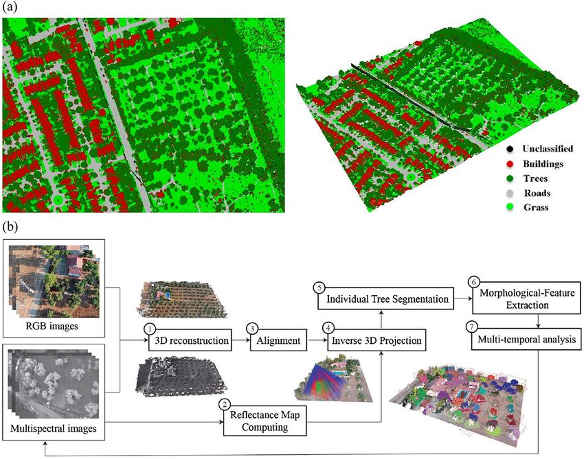
spectral LIDAR road image is shown in Figure 3(a), which is Additionally, a thermal camera is used as a secondary
captured at 905 and 1550 nm wavelengths using RIEGL vision sensor in the study by Choi et al. [20], and brings
VUX-1HA line scanning LIDAR and RIEGL miniVUX-1UAV along the advantage of capturing road images regardless of
line scanning LIDAR, respectively [18]. Within the image, daylight illumination condition. The integration of the 3D
the two-lane road can be clearly seen with details including LIDAR (Velodyne HDL-32E) and the GPS/IMU (global
road markers, road shoulders and trees around the road. positioning system/inertial measurement unit) onto the
The schematic of the multispectral imaging setup is same sensor system enables capturing of the depth infor-
shown in Figure 3(b). The multispectral LIDAR system mation and location information, respectively. Further-
together with an imaging system have been mounted on more, in the study by Takumi et al. [19], multispectral
top of a vehicle. The multispectral road data have been images covering visible, near infrared (NIR), MIR and far
collected for road area semantic segmentation. Different infrared (FIR) wavelength range are collected. These im-
road areas, including asphalt road, gravel road, highway ages are used for object detection in traffic scenes,
and parking lot, can be correctly predicted. The prediction including bike, car and pedestrian. It has been found that
1442          N. Li et al.: Spectral imaging and spectral LIDAR systems

Figure 3: Multispectral LIDAR system applied for autonomous driving.
(a) A point cloud captured by 1550 and 905 nm line-scanning LIDAR systems RIEGL VUX-1HA and RIEGL miniVUX-1UAV, respectively.
(b) Schematic of LIDAR measurement setup, showing a multispectral LIDAR system, visible camera, and GPS mounted on top of the vehicle
for data collection. (c) Road area prediction examples in comparison with the ground truth. (a)–(c) are adapted from the study by Taher [18]
with permission. Copyright Josef Taher, Finnish Geospatial Research Institute FGI.

the images at different spectral range are suitable for                   biomolecules. In order to obtain the spectral information
detection of different classes of object. Hence, the advan-               from biosamples, there are four main scanning approaches
tage of multispectral imaging for diversified object detec-                used: whiskbroom (spatial scan on both axes), pushbroom
tion has been demonstrated in the work.                                   (spatial scan on one axis), staring (spectral scan) and
                                                                          snapshot (no scan). The study by Li et al. [2] presents a good
                                                                          summary and comparison of the advantages and disad-
2.3 Biomedical spectral imaging and                                       vantages for these scanning approaches.
    sensing                                                                    In medical application, spectral imaging is mainly
                                                                          used for disease diagnosis and surgical guidance [22]. For
As mentioned in Section 1, spectral imaging system can                    disease diagnosis, multispectral optoacoustic tomography
capture an image stack by using different wavelengths,                    (MSOT) is an emerging technology, enabled by the devel-
and obtain the spectral information, including reflectance                opment of NIR high-speed tunable lasers [46]. It enables in-
and transmittance, for each pixel in the image from the                   depth high-resolution imaging and spectral information of
data cube. Such information can be used to monitor the                    tissue molecules. A recent example reported in the study by
changes of biosamples that cannot be obtained using the                   Neuschmelting et al. [37] uses MSOT for brain tumor
traditional gray-scale or RGB imaging technique [2]. The                  delineation. The stability of the nanostar contrast agent is
principle is based on the spectral signature of different                 also found through the MSOT spectra in the NIR wave-
biosamples, which originates from the interaction between                 length regime. Besides brain tumor, MSOT has also been
the multiwavelength electromagnetic waves and the                         recently applied for visualization of Alzheimer’s disease in
N. Li et al.: Spectral imaging and spectral LIDAR systems   1443

mouse’s brain [38] and pathophysiological procession [47].         earlier, in the study by Steiner et al. [23], the multispectral
Furthermore, a hyperspectral endoscopy system has been             imaging at SWIR has been applied for face recognition and
developed [48], which enables image distortion compen-             skin authentication. The images at wavelengths of 935,
sation for flexible endoscopy in clinical use. High spatial         1060, 1300 and 1550 nm are used simultaneously for anti-
and spectral resolutions have been achieved under free-            spoofing purpose. The schematic of the imaging system is
hand motion.                                                       illustrated in Figure 4(b). The light-emitting diodes (LEDs)
     For surgical guidance application, a recent example is        with different wavelengths are distributed on the illumi-
reported in the study by Hu et al. [21]. In this work, multi-      nation panel around the sensor camera. These LEDs are
spectral fluorescence imaging in visible, NIR-I (700–               programmed using microcontroller to switch on/off in
900 nm) and NIR-II (1000–1700 nm) wavelength ranges                chronological order, with only one wavelength switched
have been used to monitor the in-human liver-tumor sur-            on at any given time. An SWIR camera (with InGaAs sensor)
gery. The work shows that the NIR-II wavelength regime is          is placed in the center of the LED array to collect the re-
able to provide tumor detection with higher sensitivity,           flected light from the human face. The images captured by
signal distinction ratio and detection rate compared with          the camera are transmitted to personal computer, and
the traditional NIR-I wavelength regime. Also, with the            processed to compose a multispectral image stack. The
development of artificial intelligence and machine                  image processing steps include nonlinear correction, mo-
learning technology, it has recently been applied in the           tion     compensation,       distortion      correction      and
hyperspectral imaging system for precise cancer tumor              normalization.
detection during surgical operations [49, 50]. For example,             A part of the images taken for facial recognition are
in the study by Fabelo et al. [49], a classification method for     illustrated in Figure 4(c) and (d). In Figure 4(c), the first and
hyperspectral imaging system has been developed to                 second rows are the facial images taken in visible and SWIR
accurately determine the boundaries of brain tumor during          wavelength, respectively. By comparing the images in
the surgical operation, which is able to help the surgeon to       these two rows, it can be observed that the SWIR images are
avoid extra excision of the normal brain tissue or leaving         insensitive to different skin tones, due to the similar
residual tumor unintentionally.                                    remission spectrum in SWIR wavelength region as shown
                                                                   in Figure 4(a). Furthermore, Figure 4(d) shows a human
                                                                   face wearing 3D-printed mask acting as presentation
2.4 Biometric sensor systems                                       attack. The image in SWIR can clearly distinguish the
                                                                   human skin and printed mask, and hence illustrates the
Biometric sensors have drawn an increased attention, due           advantage of antispoofing capability of SWIR wavelength
to its wide applications covering from homeland security to        regime.
consumer electronics. Multispectral biometric system                    Furthermore, in the study by Vetrekar et al. [24], a low
enables the capturing of biometric data under different            cost multispectral facial recognition system has been
illumination levels, with antispoofing functionality and           demonstrated. The system consists of a filter wheel with
resistant to weather and environmental changes. These              nine different bands covering from 530 nm up to 1000 nm,
biometric data are typically taken from face, finger, palm or      and mounted in front of a complementary metal-oxide-
iris, followed by pattern recognition from 2D images               semiconductor (CMOS) camera. The multispectral images
captured under different spectral bands.                           taken from the CMOS camera are then fused using image
     Within a multispectral facial recognition system, the         fusion techniques, including wavelet decomposition,
wavelength range plays a significant role. Figure 4(a)             averaging, and then inverse wavelet transform. The mul-
shows the remission spectrum of different skin types and           tispectral feature of the system enables the reduction of the
spoofing mask materials from visible to NIR wavelength              illumination effect compared with single spectral system.
regime. It can be observed that human skin has relatively          An additional noteworthy point to mention on facial
lower remission at the wavelength beyond visible range             recognition is that the COVID-19 outbreak will further boost
[23]. Hence, such wavelength range can be used to sense            the need for facial recognition technology due to its con-
and distinguish skin from different materials for presen-          tactless detection scheme, which will effectively address
tation attack detection purpose. Also, different skin colors       the hygiene and infection-related issues.
have very similar remission across the wavelength between               Besides facial recognition, the fingerprint sensor is
900 and 1600 nm. Therefore, facial recognition operating           also one of the most widely deployed sensors for biometric
in such wavelength range will not be affected by the skin          identification. Different physical mechanisms have been
tone. Based on the remission (or reflection) data mentioned         implemented to capture the fingerprint information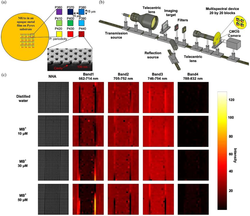
1444           N. Li et al.: Spectral imaging and spectral LIDAR systems

Figure 4: Multispectral imaging applied for facial recognition showing advantage of anti-spoofing.
(a) Remission spectrum of different skin types and spoofing mask materials from visible to NIR wavelength. (b) Schematic of multispectral
facial recognition system setup, including LED arrays at four different wavelengths (935, 1060, 1300 and 1550 nm) as light source (right panel),
and a short wavelength infrared (SWIR) camera for image capture. (c) Facial images captured with visible (first row) and SWIR (second row)
wavelengths of different skin types. SWIR images are insensitive to different skin tones. (d) Facial images with a printed mask in visible (top)
and SWIR (bottom) wavelength. The mask material can be clearly distinguished in SWIR image. (a)–(d) are adapted with permission from the
study by Steiner et al. [23]. Licensed under a Creative Commons Attribution.

including optical imaging, capacitive imaging and ultra-                   effectively. It is able to capture the images under different
sonic sensing [51–54]. However, most systems have issues                   optical wavelengths and collect data on both surface and
in detection under various circumstances, such as wet/dry                  subsurface, contributed by the fact that different wave-
finger, poor contact and susceptibility to spoofing. The                     lengths have different penetration depths within the finger
multispectral fingerprint system addresses these issues                     skin. The subsurface information also can tell whether the
N. Li et al.: Spectral imaging and spectral LIDAR systems   1445

fingerprint is from a real finger or a fake one with only 2D          imaging systems applied in archaeology and art conser-
information. The working principle of multispectral                 vation has been reported in 2012 [25]. Here we review the
fingerprint imaging has been presented in the study by               most updated work in the past decade.
Rowe et al. [55]. A commercial multispectral fingerprint                  Recently, studies on compact hyperspectral camera
sensing product (J110 MSI) has also been presented in the           from SPECIM for imaging of art work have been conducted
study by Rowe et al. [55] based on the working principle            [43, 56]. In the study by Picollo et al. [43], the new com-
introduced. The commercial product has four LEDs at 430,            mercial hyperspectral camera working from 400 to
530, 630 nm and white light. There is also an embedded              1000 nm has been used for inspection of art works. The
processor within the system for data processing.                    camera with a size of 207 × 91 × 126 mm3 has been used to
     Furthermore, due to COVID-19, as mentioned earlier in          analyze both indoor painting (a 19th century canvas
facial recognition part, touchless fingerprint imaging sys-         painting), outdoor painting (Sant’ Antonino cloister at the
tem will be highly attractive, since it helps to prevent the        Museum of San Marco, Florence), and a manuscript
spread of disease through use of same systems by multi-             (a 15th century Florentine illuminated book in Florence).
users such as lift buttons. In the study by Hussein et al.          This proves the capability of the hyperspectral camera to
[40], a novel touchless fingerprint capture device has been          operate effectively under different environmental condi-
introduced, using multispectral SWIR imaging and laser              tions. The pigment identification has been achieved
speckle contrast imaging for sensing and presentation               through the spectral angle mapper procedure embedded
attack detection.                                                   in the camera software. Furthermore, in the study by
     For iris recognition, in the study by Zhang et al. [39], a     Daniel et al. [26], hyperspectral camera working in the
multispectral imaging system has been introduced. It                same wavelength range has been used to analyze the
extends the traditional 850 nm wavelength for iris                  paintings from Goya in a Spanish museum Zaragoza.
recognition to shorter wavelength in which pigments can             Restored zoom is shown in the infrared hyperspectral
be used as another source of iris texture. The schematic of         image. The pigment identification has also been demon-
the system is illustrated in Figure 5(a) left panel. It con-        strated in the work.
tains capture unit, illumination unit, interaction unit and              Moving beyond 1000 nm wavelength, in the study by
control unit. The data collection process is illustrated in         Mahgoub et al. [42], a pushbroom hyperspectral imaging
the photograph provided in Figure 5(a) right panel. The             system (GILDEN Photonics) working in 1000–2500 nm has
system is able to capture the multispectral images in 2–3 s.        been applied to investigate an Islamic paper. A calibration
The captured multispectral images at 700, 780 and                   model has been made for the quantitative analysis. The
850 nm are shown in Figure 5(b). These images are fused             starch within the Islamic paper has been identified, and the
to form the final measurement image including all the                cellulose degree of polymerization has been quantified,
pigment information obtained from the three different               which provides information on the conservation condition
wavelengths.                                                        of the paper. Also, in the study by Cucci et al. [57], NIR
     Palmprint is also a unique biometric character, which          hyperspectral images of Machiavelli Zanobi painting have
can be applied to authentication system. Zhang et al. [41]          been obtained from 1000 to 1700 nm. From the NIR image,
proposed an online multispectral palmprint system for               the restoration places can be found which is not observable
real-time authentication. Since different band contains             from the image in visible wavelength. From the reflectance
different texture information, the combining of the bands           spectra, it is found that gypsum has been used as ground
enables detection with reduced error rate and antispoofing           layer for the painting (preparatory drawing).
functionality.

                                                                    3 Nanophotonics-based spectral
2.5 Archaeology and art conservation
                                                                      imaging and LIDAR sensing
Spectral imaging has been used as a novel and noninvasive             systems
method for archeology and art conservation since 1990s
based on [25]. Besides the 2D spatial information, it is able       Although there are many modern applications of the state-
to obtain the spectral information of the object such as an         of-the-art spectral imaging and spectral LIDAR systems as
antique, art painting or manuscript, and hence reveals the          mentioned in the previous section, most of these systems
historical and hidden information of the object. A                  are still bulky, heavy and consume high power. Hence,
comprehensive review for multispectral and hyperspectral            there is an enormous demand for compact and low-cost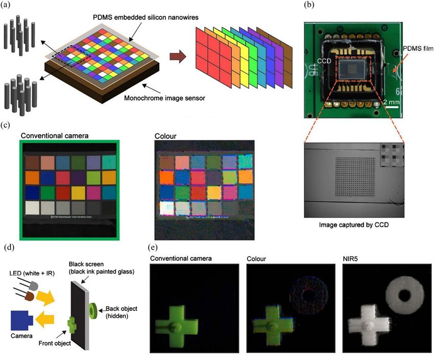
1446           N. Li et al.: Spectral imaging and spectral LIDAR systems

Figure 5: Multispectral iris recognition system and data fusion process.
(a) Schematic drawing of multispectral iris capture device (left) and an optical image showing data collection process (right). (b) Fusing
process of multispectral iris images at 700, 780 and 850 nm, including all the pigment information within iris. (a)–(b) are adapted with
permission from Springer Nature: Multispectral Biometrics, by Zhang et al. [39]. Copyright 2016.

sensing system. Nanophotonics technology [58], which is                    nanophotonics-based spectral imaging and LIDAR systems
based on light–matter interaction at nanoscale di-                         have also accelerated [28, 29, 66–69]. Various compact
mensions, provides an ideal solution. Numerous compact                     devices have been developed for the proof-of-concept
optics and photonics functional devices have been                          demonstration in this field. In this section, we have
demonstrated using CMOS-compatible fabrication process                     reviewed these research works on nanophotonics-based
[59–65]. In the past decade, research works on                             spectral imaging and LIDAR sensing systems. Subsection
N. Li et al.: Spectral imaging and spectral LIDAR systems 1447
3.1 is mainly focused on the spectral imaging systems that 3.1 Spectral imaging systems
have been demonstrated in the past decade. Subsection
3.2 is focused on the most recent research works of 3.1.1 Metasurface-based lens and reflectors
nanophotonics-based LIDAR systems using integrated
frequency comb or supercontinnum as light source. Flat optics or metasurface [80, 81], which can be formed by
Also, the reviewed works are categorized based on ma- a single layer of subwavelength-scale nanostructures, has
terial, structure, sensing mechanism and working drawn a lot of research interests in the field of nano-
wavelength, as listed in Table 2. photonics. It works based on the scattering of light by the
Table : Summary of nanophotonics-based spectral imaging and LIDAR sensing systems.
Material and structure Sensing mechanism Application Wavelength Reference/
year
Elliptical amorphous silicon (a-Si) Hyperspectral imaging Immunoglobulin G (IgG) biomolecule detec- – nm []/
nanobars on fused silica tion and sensing with high sensitivity
substrate
TiO-based metasurface Multispectral imaging Chiral beetle multispectral imaging using sin- , , and []/
gle metalens to resolve the chirality nm
Periodic silver nanowires Multispectral imaging Tunable color filter with polarization – nm []/
dependent transmission for color imaging
a-Si nanoposts with rectangular Hyperspectral imaging Hyperspectral imaging with compact size and – nm []/
cross section on silica substrate light weight
Periodic silicon pillar with Hyperspectral imaging CMOS-compatible, low cost and compact – nm []/
photonic crystal structure hyperspectral imaging system
Bayer color filter array Multispectral imaging Multispectral imaging for early stage , , , []/
pressure ulcer detection and nm
SiN-AlN-Ag multilayer stack to Multispectral imaging Color image using metal-dielectric filter – nm []/
form Bayer color filter array patterned in Bayer array on CMOS image
sensor (CIS)
Microscale plate-like SiN Multispectral imaging Color imaging using near-field deflection- – nm []/
structure based color splitting with minimal signal loss
Si nanowire Multispectral imaging All-silicon multispectral imaging system in – nm []/
visible and NIR wavelength
Periodic circular holes on gold Multispectral imaging Adaptive multispectral imaging using plas- – μm []/
(Au) layer monic spectral filter array working in LWIR
Nanohole arrays in an Au film Multispectral imaging Multispectral imaging of methylene blue for – nm []/
transmission-imaging and leaf for reflection-
imaging
Periodic circular holes on Al thin Multispectral imaging Multispectral imaging using plasmonic spec- – nm []/
film tral filter array integrated with CMOS-based
imager
Elliptical and circular hole arrays Multispectral imaging Low-photon multispectral imaging RGB: , , []/
on Al thin film and nm
Pixelated Si-based metasurface Imaging-based Biosensing for protein A/G .–. μm []/
with zigzag array structure spectroscopy
Silica wedge disk resonator Dual-comb based time of Distance measurement with high accuracy – nm []/
flight (ToF) LIDAR
SiN microring resonator Dual-comb based LIDAR Distance measurement at high speed and – nm []/
pumped by erbium-doped fiber accuracy
amplifier (EDFA)
SiN microring resonator Frequency-comb based Distance and velocity measurement along a – nm []/
pumped by EDFA FMCW LIDAR line
Terahertz quantum cascade Dual-comb based hyper- Bio-imaging ., ., and []/
lasers spectral imaging . THz1448 N. Li et al.: Spectral imaging and spectral LIDAR systems
nanostructures. These nanostructures, also called as the spectral information. The full-Stokes polarization im-
nanoantennas, can be patterned to achieve designed aging with compact optical system enabled by metasurface
spectral response or phase profile, thereby enabling varied has later been demonstrated [104, 105], in which additional
functional devices such as lenses [82, 83], spectral filters information including the mechanical stress of the sensing
[84, 85], wave plates [86, 87], beam deflectors [88–90] and object and texture of reflecting surfaces are also revealed. A
point cloud generator [91]. For metalens, when the phase of comprehensive review on recent advances of metasurface-
the scattered light from nanoantennas follow the hyper- based polarization detection has been published in the
boloidal profile below, the scattered light will focus at one study by Intaravanne and Chen [106].
point [81, 82]: Also, contributed by the capability of dispersion con-
trol with metasurface, in the study by Faraji-Dana et al.
2π √̅̅̅̅̅̅̅̅̅
φ= ( x2 + y2 + f 2 − f ) (1) [68], a line-scanned hyperspectral imager with a single-
λ
layer metasurface, which is patterned by a single-step
where λ is the wavelength in free space, f is the focal length lithography process on glass substrate, has been demon-
of the metalens. While for reflectors, the angle of reflected strated, with schematic shown in Figure 6(c) left panel. The
light follows the generalized Snell’s law for reflection [80]: imaging system is based on a compact folded metasurface
platform [107]. The light from the object enters the system
λ dφ
sin( θr ) − sin( θi ) = (2) from an aperture at the top, reflects between the meta-
2πni dx
surfaces and gold mirrors, and finally exits from the
where θr and θi are reflection angle and incident angle, transmissive metasurface at the bottom for image forming.
respectively. ni is the refractive index of the media. dφ/dx is The imaging system is designed to disperse the light with
the gradient of phase discontinuity along the reflection different wavelengths in vertical direction. The light with
interface. Such phase discontinuity can be engineered to different incident angles along the horizontal direction is
achieve the designed reflection angle of the optical beam. focused horizontally at the detector array. The Caltech logo
The integration of metasurface devices with active layers has been used for imaging as a proof-of-concept demon-
enables the active tuning and control of optics [92–96]. stration, with simplified setup schematic shown in
Furthermore, the metasurface can also be engineered to Figure 6(c) right panel. The inset shows the colored Caltech
achieve desired dispersion [97]. Metasurface-based achro- logo with wavelength increasing from bottom (750 nm) to
matic optical devices have been demonstrated [98–103], top (850 nm). The imaging results are illustrated in
which can be applied for multispectral imaging. In the Figure 6(d). The left panel shows the intensity profile ob-
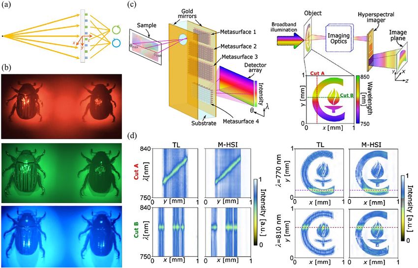
study by Khorasaninejad et al. [70], a single metasurface- tained by metasurface hyperspectral imager (M-HSI) along
based lens (metalens) has been used to replace the so- cut A and cut B. The result is benchmarked with the one
phisticated ensemble of optical components to achieve obtained by a tunable laser (TL), and shows a good match.
simultaneous imaging in two opposite circular polarization The intensity of the two wavelengths 770 and 810 nm ob-
states. The schematic of the setup is shown in Figure 6(a), tained by M-HSI are shown in Figure 6(d) right panel. It is
illustrating the imaging principle: the light with different also compared with the result obtained by TL, showing a
circular polarizations from object is focused by the multi- good match.
spectral metalens at different physical locations for imag-
ing purpose. The multispectral images of chiral beetle 3.1.2 Spectral filters integrated with photodetector
(Chrysina gloriosa), which is known for high reflectivity for array or CMOS camera
only left-circularly polarized light, are also illustrated in
Figure 6(b). These images are obtained by using LEDs at Besides the metasurface-based lens and reflectors used in
red, green and blue color together with a band pass filter at the earlier works, the spectral filters made from flat optics
each wavelength. The compact multispectral imaging can also be placed on top of a photodetector (PD) or a CMOS
system reported in the study by Khorasaninejad et al. [70] image sensor (CIS) for spectral imaging. A recent work to
should be able to obtain the helicity and spectral infor- integrate the spectral filter with a PD array has been re-
mation from other biosamples as well. An additional point ported in the study by Shah et al. [33]. In this work, a
worth mentioning is that, besides the spectral information, plasmonic metasurface-based color filter with elliptical
the study by Khorasaninejad et al. [70] also illustrates that and circular nanoholes are defined in a thin Aluminum (Al)
extra information of the sensing object can be obtained layer. To achieve different resonance wavelengths in
through the polarization of light. Hence, polarization pro- visible range, the dimension of these sub-wavelength scale
vides one more degree of freedom in imaging in addition to nanoholes are varied, as shown in Figure 7(a) where theN. Li et al.: Spectral imaging and spectral LIDAR systems 1449 Figure 6: Metasurface-based lens and reflectors for spectral imaging. (a) Top panel: schematic illustration of the multispectral metalens imaging principle: the light from object with different circular polarizations is focused at different location by the multispectral chiral lens. (b) The beetle (Chrysina gloriosa) images formed by using red, green and blue LED illumination together with a band pass filter at each wavelength. (a) and (b) are adapted with permission from the study by Khorasaninejad et al. [70]. Direct link: https://pubs.acs.org/doi/10.1021/acs.nanolett.6b01897. Further permissions related to the material excerpted should be directed to the ACS. (c) Left panel: the schematic of the hyperspectral imaging system: the light from sample enters the system through the aperture at the top, then is reflected between the metasurfaces and gold mirrors, and exits through the transmissive metasurface at the bottom. On detector array, light with different incident angles is focused along the horizontal direction, and light with different colors is focused along the vertical direction. Right panel: the simplified schematic of the system for imaging the object. Inset shows the object of Caltech logo with mixed color, whose wavelength increases from bottom (750 nm) to top (850 nm). (d) Left panel: measured intensity profile captured by photodetector (PD) across cut A and cut B by the metasurface hyperspectral imager (M-HSI). M-HSI imaging result is benchmarked with the intensity profile obtained using a tunable laser (TL). Right panel: measured intensity at two wavelengths (770 and 810 nm) by M-HSI benchmarked with the one obtained using TL. (c) and (d) are adapted with permission from the study by Faraji-Dana et al. [68]. Direct link: https://pubs.acs.org/doi/full/10.1021/acsphotonics.9b00744. Further permissions related to the material excerpted should be directed to the ACS. scanning electron microscopy (SEM) images of the nano- of 33.33%. The active imaging system utilizes a super- structures are illustrated. The inset of the figure shows the continuum tunable laser source, whose schematic is micrograph of the color filter. The filter array is patterned shown in Figure 7(c). As a proof-of-concept demonstration, by a single-step electron beam lithography. Once the the color image of a sample target taken by conventional fabrication is completed, the filter array is then integrated camera and the reconstructed image obtained from the with a 64 × 64 single photon avalanche photodetector multispectral imaging system are illustrated in Figure 7(d) (SPAD) array through a flip-chip bonding process. Hence, left and right panel, respectively. The sensing system the imaging system has the capability of counting at single demonstrated in this work can find applications in photon level. The optical images of the system are illus- LIDAR-based 3D imaging. trated in Figure 7(b). Each filter covers one of the 64 × 64 A recent demonstration for integration of dielectric pixels of SPAD, with red, green and blue colors randomly metasurface-based spectral filter with a CIS is also reported distributed. Each color has approximately equal quantity in the study by Yesilkoy et al. [67]. In this work, a
1450           N. Li et al.: Spectral imaging and spectral LIDAR systems

Figure 7: Metasurface-based plasmonic color filters integrated with single photon avalanche photodetector (SPAD) array for spectral imaging.
(a) Scanning electron microscopy (SEM) images of the fabricated color filters, with inset illustrating the micrographs of blue-, green- and red-
colored filter. (b) Optical image of color filters integrated with SPAD array. (c) Schematic of the imaging system, including the supercontinuum
tunable laser as light source. (d) Left panel: sample target used for multispectral imaging. Right panel: reconstructed multispectral image of
the sample target. (a)–(d) are adapted with permission from the study by Shah et al. [33]. Licensed under a Creative Commons Attribution.

biomolecule sensor has been demonstrated based on                          nanophotonics-based spectral filters can be integrated
hyperspectral images taken by high quality factor dielectric               with CCD or CIS, either through attaching on the image
metasurface integrated on a CIS. The sensing mechanism is                  sensor [27, 29, 73, 76] or direct patterning on the image
illustrated in Figure 8(a). A tunable narrow-band laser                    sensor [72, 108–110]. The compact integrated system is a
source, formed by a tunable filter coupled to a super-                      suitable platform for spectral imaging. In the study by
continuum light source, is used to illuminate the meta-                    Park and Crozier [27], a compact multispectral imaging
surface with immunoglobulin G (IgG) solutions. The                         system has been demonstrated by using color filters
spectral information of each pixel can be obtained from the                formed by vertical silicon nanowires. The color spec-
hyperspectral data cube, as shown in bottom right panel of                 trum is varied by the nanowire diameter. The nano-
Figure 8(a). The resonance wavelength shift of the meta-                   structures are patterned by a single-step electron beam
surface induced by the IgG molecules can be obtained by                    lithography process. The nanowires embedded in poly-
comparing the spectral information to the reference without                dimethylsiloxane (PDMS) is attached to a Si-based image
the IgG molecule. Higher IgG biomolecule concentration                     sensor, with schematic and optical image shown in
contributes to larger refractive index change and hence larger             Figure 9(a) and (b), respectively. The zoomed-in image of
resonance wavelength shift of the metasurface. In this way,                the fabricated nanowire filter array is included at the
the concentration information of the IgG can be obtained.                  bottom of Figure 9(b). In the imaging system, there are five
Figure 8(b) shows the schematic of the bioassay for IgG                    channels in visible range and three channels in infrared
biomolecule binding/immobilization process. The mean                       (IR) wavelength range. In Figure 9(c), left and right panels
resonance wavelength shifts with respect to different IgG                  show the image of Macbeth color chart obtained using
concentrations have been plotted in Figure 8(c).                           conventional camera and three channels of this multi-
     The CIS mentioned above has been widely applied                       spectral imaging system in visible range, respectively.
due to its advantages including compact size, low cost,                    The colors show good match. Furthermore, the advantage
low power consumption and ease of integration with                         of IR channel is demonstrated using the experiment setup
other CMOS-based functional devices. Rather than using                     shown in Figure 9(d). A donut-shaped object is placed at
CIS and spectral filter as separate components, the                        the back of a black screen (glass painted with black ink),
N. Li et al.: Spectral imaging and spectral LIDAR systems 1451 Figure 8: Dielectric metasurface-based hyperspectral imaging for ultrasensitive biomolecule detection. (a) Schematic of dielectric metasurface-integrated CIS for hyperspectral imaging-based biosensing. Narrow-band tunable laser source is used for illumination. CMOS camera captures image for each wavelength and the data forms hyperspectral data cube. For each pixel, the resonance wavelength can be obtained from the processed spectral information. Biosensing is achieved by comparing the resonance map of metasurface with biomolecules and the reference resonance map without the biosample. (b) Schematic showing the immobilization process of the biomolecules for sensing purpose. (c) Mean resonance shift with respect to average number of IgG molecules. (a)–(c) are adapted with permission from Springer Nature, Nature Photonics [67]. Ultrasensitive hyperspectral imaging and biodetection enabled by dielectric metasurfaces, Yesilkoy, et al. Copyright 2019. which is opaque in visible wavelength, but transparent in and right panel, respectively. From the IR image, the IR range. The images obtained by the system in visible and donut-shaped object can be observed. For comparison, IR wavelength range are shown in Figure 9(e) middle the image taken by a conventional camera in visible
1452           N. Li et al.: Spectral imaging and spectral LIDAR systems

Figure 9: Si nanowire-based spectral filter integrated with CCD image sensor for multispectral imaging in visible and infrared (IR)
wavelength range.
(a) Schematic of the multispectral imaging system, with inset showing the Si nanowire structure as spectral filter. (b) Optical image of the
spectral filter mounted on CCD image sensor, with zoom-in image of the filter area at the bottom panel. Inset of the bottom panel shows the
magnified image of the filter array. (c) Image of Macbeth color chart taken by conventional color camera (left panel) in comparison with the
image taken by the nanowire-based multispectral imaging system (right panel). (d) Schematic of imaging setup using white light and IR LED as
light source to demonstrate the advantage of multispectral imaging. (e) Images taken by conventional camera (left), nanowire-based imaging
system in visible wavelength range (middle), and nanowire-based imaging system in IR wavelength range (right). The donut-shaped object at
the back of the black ink painted glass is invisible or hard to observe from the image in visible wavelength, but can be observed from the image
in IR wavelength. (a)–(e) are adapted with permission from the study by Park and Crozier [27]. Licensed under a Creative Commons Attribution.

wavelength range is shown in Figure 9(e) left panel,                       visible wavelength range. Based on the same material
where the cross-shape object in front of the screen can be                 platform, in the study by Burgos et al. [76], the plasmonic
clearly observed, while the donut-shaped object at the                     color filter array has been integrated with a CIS to
back of the screen is hardly seen.                                         demonstrate a plasmonic-based full-color imaging func-
     Besides the abovementioned metasurface-based de-                      tionality. The schematic of the CIS with RGB plasmonic-
vice integration with image sensor, in the study by Yoko-                  based filters on top is shown in Figure 10(a) left panel. The
gawa et al. [111], the plasmonic-based color filter array                   SEM image of the filters, the optical image of the filter array
designed for CIS has also been demonstrated, which has                     on quartz substrate, and the integrated CIS have been
potential application for spectral imaging. The color filters               included in Figure 10(a) right panel. The Al nanostructure
are formed by hole arrays on 150-nm thick Al film to work in                is patterned using a single-step electron beam lithography
N. Li et al.: Spectral imaging and spectral LIDAR systems 1453
followed by a lift-off process on quartz substrate. The achieve different resonance frequency. The spectrum of
fabricated structure is then integrated with the CIS through light source can hence be reconstructed. Figure 10(d)
a contact process. The reconstructed image of a 24-patch shows some reconstructed optical spectrum plotted in blue
Macbeth color chart obtained from the integrated system is circles well matched with the reference ground-truth
shown in Figure 10(b) right panel, showing good match spectrum plotted in red solid line. The hyperspectral
with the image taken by conventional CMOS camera shown functionality has also been demonstrated, as shown in
in Figure 10(b) left panel. Figure 10(e). Two numbers “5” and “9” are illuminated by
Also, using the same contacting/assembly approach, light source at 610 and 670 nm, respectively. The target on
the photonic crystal has been implemented as spectral the screen is a superposition of “5” and “9” encoded using
filter for spectral imaging. In the study by Wang et al. [29], a these two wavelengths. The hyperspectral image stack
compact on-chip spectrometer with hyperspectral imaging shown on right panel of Figure 10(e) is able to distinguish
functionality has been demonstrated, whose schematic is two numbers at different wavelengths, which is not
shown in Figure 10(c). The photonic crystal array is fabri- distinguishable using the conventional RGB camera. An
cated and then attached on top of the CMOS sensor array. additional note from the authors of this work is that the
The photonic crystal dimension for each slab is varied to pixel number in this hyperspectral imager is limited by the
Figure 10: Metallic and dielectric nanophotonics spectral filters integrated with CMOS sensor for spectral imaging.
(a) Schematic of hole array-based RGB spectral filter integrated with CIS, with inset showing the SEM image of the filter array, optical images of
the filter array patterned on quartz substrate, and the optical image of the integrated system. (b) Image of Macbeth color chart taken by
conventional CMOS camera (left panel) and the plasmonic-based CMOS camera (right panel) for comparison. (a)–(b) are adapted with
permission from the study by Burgos et al. [76]. Copyright © 2013 American Chemical Society. (c) Schematic of microspectrometer consisting
photonic-crystal array integrated with CMOS sensor array. (d) Measured optical spectrum from a narrow-band light source centered at
581–584 nm by the integrated spectrometer. The measured results plotted in blue circles are benchmarked with the ground-truth data plotted
in red solid line, showing good match. (e) Left panel: hyperspectral imaging setup using photonic-crystal-based spectral imaging system.
The target on the screen is a superposition of “5” and “9” encoded using different wavelengths. Right panel: the captured images at different
wavelengths, where “5” and “9” can be distinguished at wavelength of 610 and 670 nm, respectively. (c)–(e) are adapted with permission from
the study by Wang et al. [29]. Licensed under a Creative Commons Attribution.You can also read