Tutorial 1 - Introduction to ASIC Design Methodology
←
→
Page content transcription
If your browser does not render page correctly, please read the page content below
Tutorial 1 - Introduction to ASIC Design Methodology
                         ECE-520/ECE-420 ~ Spring 1999 ~ Rev. 99.1
                        Dr. Paul Franzon, Scott Perelstein, Amber Hurst
--------------------------------------------------------------------------------------------------------------------

1 Introduction:
Typical ASIC design flow requires several general steps that are perhaps best illustrated using a
process flow chart:
                                Figure 1: Process Flow Chart
                             HDL Design Capture
                                                      Design Specification

                                                     Behavioral Description

                                                       RTL Description

                                                             RTL
                                                                              No
                              Verification Vectors       Functionality
                                                           Verified?

                                                                 Yes
                             HDL Design Synthesis
                                                         RTL to Logic

                                 Constraints          Logic Optimization

                                                      Logic to Technology

                                                         Timing/Area
                                 Constraints
                                                         Optimization

                                                      Scan Path Insertion &
                                                     Test Vector Generation

                                                           Netlist
                                                                              No
                                                        Logic & Timing
                                                           Verified?

                                                                 Yes
                             Design Implimentation
                                                        Floor Planning

                                                         Place & Route

                                                        Physical Layout

                                                            Layout
                                                                              No
                                                       Function & Timing
                                                           Verified?

                                                                 Yes
                                                        Chip Production

                                                            1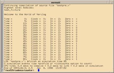
This tutorial is meant only to provide the reader with a brief introduction to those portions of the
design process that occur in the HDL Design Capture and HDL Design Synthesis phases, and a
brief overview of the design automation tools typically used for these portions of the design pro-
cess. The detailed methodology and strategies required to produce successful designs will be dis-
cussed throughout the course lectures.

This tutorial is broken up as follows:
   • Section 2 is an overview of the design, synthesis and verification process
   • Section 3 is an overview of the tools to be used
   • Section 4 discusses pre-synthesis simulation and verification using Verilog. This step is
       important to ensure that your Verilog input for Synopsys is correct.
   • Section 5 discusses logic synthesis using Synopsys. This is the step in which the Ver-
       ilog code is converted to a gate level design.
   • Section 6 discusses post-synthesis simulation and verification using Verilog. This sim-
       ulation is run to check that the above two steps were correctly conducted.
   • Section 7 discusses post-synthesis timing verification using Cadence Pearl. This timing
       verification is carried out as a check on the timing of the gate level design produced by
       Synopsys.
   • Section 8 discusses how to run these tools using scripts. Most of the discussion in Sec-
       tions 4-7 are centered on running these tools interactively. Sometimes these tools can
       take a long time to run and running the tool in batch mode using a script is useful.
   • Section 9 summarizes how to run the tools remotely. You can do all of the stepts above
       over a telnet session if you want.
   • Section 10 discusses the Veriwell PC Verilog simulator. You can download this simula-
       tor and use it instead of Verilog-XL for pre-synthesis simulations.

2 The Design Process:
Referring to the figure on the previous page, the HDL Design Capture phase implements the “top-
down” methodology of design. It takes a designer from abstract concept or algorithm down to
hardware in manageable and verifiable steps. This involves developing a design specification that
will be used to create a high level behavioral abstraction with high-level programming languages
such as C/C++. Additionally, this model may also be created using the Verilog hardware descrip-
tion language (HDL). The behavioral model should be simulated in order to verify that the desired
functionality is captured completely and correctly. The behavioral abstraction is then used as a
reference to create and refine a synthesizable register transfer level (RTL) abstraction that cap-
tures the desired functionality required by the design specification.

With Verilog, the difference between a purely “behavioral” and an RTL abstraction may appear
subtle at this point, but it is important that you come away from the course with a clear under-
standing of the distinction between them. Generally, we will represent designs in Verilog at three
levels of abstraction:
    • The Behavioral Level: a design is implemented in terms of the desired algorithm, much
       like software programming and without regard for actual hardware. As a result, a Ver-
       ilog model written at the behavioral level usually can not be synthesized into hardware
       by the synthesis tools.

                                                 2
• The Register Transfer Level: a design is implicitly modeled in terms of hardware regis-
     ters and the combinational logic that exists between them to provide the desired data
     processing. The key feature is that an RTL level description can be translated into hard-
     ware by the synthesis tools.
   • The Structural Level: a design is realized through explicit instances of logic primitives
     and the interconnects between them, and is also referred to as a “gate-level” model.

The HDL Design Capture phase is completed with “pre-synthesis” simulations to verify that the
RTL abstraction fully provides the desired functionality. The functional verification of the design
that occurs at this point must be as complete and thorough as possible. This requires that the
designer fully understand both the design specification and the RTL implementation. The test vec-
tors employed during simulation should provide the coverage necessary to ensure the design will
meet specifications.

The HDL Design Synthesis phase involves using a synthesis tool to:

   • Translate the abstract RTL design description to register elements and combinational
     logic,
   • Optimize the combinational logic by minimizing, flattening and factoring the resulting
     boolean equations,
   • Translate the optimized logic level description to a gate level description using cells
     from the specified technology library,
   • Optimize the gate level description using cell substitution to meet the specified area and
     timing constraints, and
   • Produce a gate level netlist of the optimized circuit with accurate cell timing informa-
     tion.

HDL Design Synthesis finishes with “post-synthesis” simulations to verify that the gate level cir-
cuit fully provides the desired functionality and meets the appropriate timing requirements.

3 Tools:
The specification for the design used in this tutorial is for a 4 bit down-counter with a inputs
named “in”, “latch” “dec” and “clock,” and an output named “zero.” The design provides the fol-
lowing functionality:
   • The internal count value is loaded from “in” on a positive clock edge only when “latch”
      is high.
   • The count value decrements by 1 on a positive clock edge when “dec” is high.
   • When the count value is 0, no further decrementing occurs.
   • The “zero” flag is active high whenever the count value is 0.

A behavioral model written using Verilog as a high level programming language may look like the
following:
              always@(latch)
              begin
                if(latch)

                                                3
value = in;
                 else
                   while (value > 0)
                   begin
                     value = value - 1;
                     zero = (value == 0);
                   end
               end

You will find files necessary for this tutorial in the ece520_info/tutorials/tutor1/bin/ locker.
These include an RTL description of a simple down counter written in Verilog (count.v), Verilog
test fixtures (testcount.v) for pre-synthesis (testpre.v) and post-synthesis (testpost.v, simpost)
functional verification, and a command script (count.dc) to guide the Synopsys synthesis tool’s
translation of the RTL description of the counter to a gate-level netlist. You will also find the ver-
ilog test fixtures (testmin.v, testmax.v) and the scripts (simmin, simmax) required to run back
annotated timing analyses. The directory also contains all the files necessary to run the static tim-
ing analysis tool, Pearl. These files include the scripts to direct Pearl (count_final.cmd, all.cmd)
and the library file (std-cell.tech). Finally there is an example script for running remotely (run-
meall).

The tutorial is separated into the following parts:
   • Section 4 “Pre-Synthesis Simulation using Stand-Alone Cadence Verilog.”
   • Section 5 “Verilog RTL Synthesis using Synopsys.”
   • Section 6 “Post-Synthesis Simulation and Timing Analysis of the Gate-Level Netlist.”
   • Section 7 “Cadence Timing Analysis Tool: Pearl.”
   • Section 8 “Running the tools in Scripts.”
   • Section 9 “Remote Use of Tools.”
   • Section 10 “PC Tools.”
   • Section 11 “References.”

The tools used for design capture may depend upon the complexity of the design being imple-
mented. Where simple designs may require only the use of the stand-alone Cadence Verilog tool
and Signalscan, more complex design will probably require the use of the Cadence Composer
tools.

4 Pre-Synthesis Simulation using Stand-Alone Cadence Verilog.
   4.1 Initial Setup.
   This section describes the steps necessary to configure your environment and obtain the files
   needed to complete this tutorial. This section will only need to be accomplished once.

   1. You are encouraged to create a directory for your ECE-520 work in your home directory.
   You should then create directories for your homework, Cadence, and miscellaneous work
   under it. The figure below illustrates this suggested hierarchy, and the sequence that follows
   will create these initial directories for you.

                                                  4
Figure 2: File Folders
eos> mkdir ~/ece520
eos> mkdir ~/ece520/cadence
eos> mkdir ~/ece520/hw
eos> mkdir ~/ece520/misc
Note: The tools that we use in this course generate a large number of files during each lab.
These files are far easier to use and maintain when they are well organized from the start. You
are therefore encouraged to follow this or some other logical plan for arranging your work.
2. The following steps will create a working directory for the down-counter design in your
Cadence locker, change your current working directory to the down-counter directory, and
copy the files required for pre-synthesis simulation to there.
eos> mkdir ~/ece520/cadence/counter
eos> cd ~/ece520/cadence/counter
eos> attach ece520_info
eos> cp /ncsu/ece520_info/tutorials/tutor1/bin/* .
Ensure that your counter directory now has the files named all.cmd, count.dc, count.v,
count_final.cmd, runmeall*, simmax*, simmin*, simpost*, std-cell.tech, testcount.v, test-
max.v, testmin.v, testpost.v and testpre.v.
4.2 Simulation using only Stand-Alone Cadence Verilog.
This section will describe the steps used to simulate and verify a design using the stand-alone
Cadence Verilog tool in a single textual interface, such as that found in a dial-up session (Sec-
tion 9 on page 26.)
1. With a text editor, open and inspect the files named count.v and testpre.v. The counter mod-
ule in count.v file is a Verilog RTL “definition” of the counter, and counter u1 contained
within the test_fixture module of the testpre.v file is an “instance” of this counter. The first line
on the testpre.v file tells the Cadence Verilog tool to include the counter definition during
compilation. Within the test_fixture module, you should also note the following “system
tasks” and their purpose:
5• $display(“text with format specifiers”, signal, signal, ...); prints the formatted mes-
sage once when the statement is executed during the simulation.
• $dumpfile(“file name”); opens/creates the named “value change dump” file for writing
the simulation results in a format that can be used later with an external viewer. See
Chapter 20 in the Verilog-XL Reference for more information.
• $dumpvars; “probes” and saves signal waveforms on all nets of the design in the
opened results file.
• $finish; finishes the simulation and exits the simulation process.
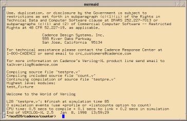
2. Enter the following at your EOS prompt:
eos> add cadence
eos> verilog testpre.v
You should see results similar to the following:
Figure 3: Verilog-XL -- First Run Pre-syntheses Results
Notice the output created by the $display(“Welcome to the World of Verilog \n”); system
task.
Note: The telephone number displayed for technical assistance from Cadence is not for use by
university students. If you need assistance, you should consult the references listed at the end
of this document.
63. Using a text editor of your choice, open the testpre.v file and un-comment the line:
$monitor(“Time =%d; Clock =%b; In =%h; Zero =%b”, $stime,
clock, in, zero);
The $monitor(“text with format specifiers”, signal, signal, ...); system task monitors the
signals listed and prints the formatted message whenever one of the signals changes.
4. Ensure you save the modified testpre.v file, then re-run the simulation by entering the fol-
lowing at your EOS prompt:
eos> verilog testpre.v
You should see results similar to the following:
Figure 4: Verilog-XL -- Second Run Pre-syntheses Results
Now note the more useful output created by the $monitor(“Time %t, ...”); system task.
Take a moment to verify that the down counter behaves as expected.
4.3 Verification using Stand-Alone Cadence with Signalscan.
This section will describe the steps used to verify a design using the stand-alone Cadence Ver-
ilog tool output in conjunction with the Signalscan graphical waveform viewer when in an X-
7Window environment.
1. Ensure that counterpre.vcd file was created during the simulation above.
2. To invoke the Signalscan waveform display tool, enter the following at your EOS prompt:
eos> signalscan &
After a moment, the following Signalscan waveform display window should appear:
Figure 5: Waveform opening window
Note: If you have not added the Cadence tools to your path during this session, you will need
to enter “add cadence” at your EOS prompt before you can use the Signalscan tool.
3. From the Signalscan window menu bar, select:
File -> Open Simulation File...
The following window should appear:
8Figure 6: Signalscan--Load Database Window
4. Set the filter in the top-line to look for *.vcd files. In the Load Database window, left-click
with the mouse to highlight counterpre.vcd in the Files box. Then left-click on the button
labeled OK. If a file translation window appears, choose OK.
5. From the Signalscan window menu bar, select:
Windows -> Design Browser
The following Signalscan Browser should appear:
Figure 7: Signalscan--Browser
6. In the box labeled Instances, select test_fixture to move down through the simulation hierar-
chy.
97. To select all of the signals, simply click and hold the left mouse button while you drag the
pointer over the desired names in the nodes/variables in current context box. This should
highlight all of the appropriate signals present at the test_fixture level of the simulation. The
Signalscan Browser window should now appear as shown:
Figure 8: Signalscan -- Browser
8. After you have highlighted the desired signals, left-click on the Add, close button
9. A graphical representation of the simulated signals should now be seen in the Signalscan
waveform display window. Left-click on the ZmOutXFull button to expand the signals to fill
the waveform display window. When you are finished, the Signalscan window should appear
similar to the one below:
Figure 9: Signalscan -- Final Waveform Display
Note: The box on the left-hand side of the waveform display window shows the corresponding
signal names. You can change the width of this box if necessary by dragging the divider
between the left-hand and right-hand sections of the window.
10You are encouraged to explore the features of this tool and in particular, note that you can save
the current setup parameters, close the waveform file, re-run the simulation, and then restore
the previous setup parameters with the new simulation results. These features are available
from the File -> pull-down menu.
10. When you are finished with the waveform display, select:
File -> Exit
from the Signalscan menu bar.
5 Verilog RTL Synthesis using Synopsys.
5.1 Initial Setup.
This section describes the steps necessary to configure your environment for using Synopsys.
This section will only need to be accomplished once.
1. Enter the following at your EOS prompt to copy the file required for configuring your sys-
tem environment to use Synopsys:
eos> cp /ncsu/ece520_info/tools/.synopsys_dc.setup ~
2. Enter the following to ensure that your root or home directory now has the file named
.synopsys_dc.setup:
eos> ls ~/.synopsys_dc.setup
5.2 Synthesis using Synopsys Design Analyzer.
This section will describe the steps used to synthesize an RTL design using the GUI Synopsys
Design Analyzer and Command Window interfaces when in an X-Window environment.
1. With a text editor, open and inspect the file named count.dc. This file contains a list of Syn-
opsys commands that will be executed sequentially by the Design Analyzer. Note that each
command has been fully commented for you so that you can recognize and understand the
steps taken during synthesis to produce an optimal design that will function properly within a
set of given constraints. Please take a moment to read carefully over the contents of this file
and note the following commands and their purpose:
• target_library = {"ms080cmosxCells_XXW.db"} specifies the library whose cells
will be used to create the netlist for the design. In this case a CMOSX worst case
library which will be used to check for setup timing violations.
• link_library = {“ms080cmosxCells_XXW.db”} specifies the library whose cells are
used in the current design netlist.
• translate replaces each cell in the current design with the closest matching functional
cell from the target library. Since no optimization takes place, a design that met timing
constraints previously may fail to once the cells are translated to the new technology
library.
• write_timing -output count_*.sdf -format sdf-v2.1 creates a separate “Standard
Delay Format” file containing timing constraint information for cells used in the
design. This is allows for “forward annotation” of the delay values to the Cadence tools
11during post-synthesis simulation.
2. To invoke the Design Analyzer tool, enter the following at your EOS prompt:
eos> add synopsys
eos> design_analyzer &
After a moment, the following Synopsys Design Analyzer window should appear:
Figure 10: Design Analyzer Opening Window
This window provides a graphical user interface to the Synopsys synthesis tool and is used to
display and interact with symbol and schematic representations of the gate level circuits that
result from synthesis. An additional window, referred to as the Command Window, is provides
a textual interface to the synthesis tool through the use of Synopsys commands.
3. To access the Command Window, select:
Setup -> Command Window...
from the Design Analyzer menu bar. After a moment, the following Command Window should
12appear:
Figure 11: Design Analyzer -- Command Window
Notice that at the bottom of the Command Window there is a box with a design_analyzer
prompt. This prompt acts as the command line for entering Synopsys commands manually.
4. Since you already have the count.dc script file containing the necessary commands for syn-
thesis, all you have to do is enter the command to tell Synopsys to include the contents of the
file. There are two ways to enter the command from within design_analyzer.
4a. The first method is to use the Design Analyzer menu bar; Select:
Setup -> Execute Script...
After a moment, the following Execute File Window should appear:
Figure 12: Design Analyzer -- Execute File Window
Left click on count.dc and choose OK.
4b. The second method is to use the Command Window. At the design_analyzer
prompt, enter:
design_analyzer> include count.dc
13Either one of these commands will cause Synopsys to read and execute the commands from
the script file. You should see the contents of the file echoed to the Command Window along
with responses from the synthesis tool. Even though these will scroll through rapidly at times,
you will still have access to the results later on since they are simultaneously echoed to a
view_command.log file in the working directory.
Note: Without exception, you must determine and correct all conditions that lead to “error”
statements. You can choose to accept conditions that lead to “warning” statements, but only
when you determine that the ramifications are acceptable within your design.
5. The script will take a few moments to run. You can determine when synthesis is complete
be observing the design_analyzer prompt in the Command Window. When a blinking cursor
re-appears, the script should have been executed completely. Your Synopsys Design Analyzer
window should now appear similar to the one pictured below:
Figure 13: Design Analyzer -- Results Window
6. In the Synopsys Design Analyzer, left click on the counter symbol in order to select it. You
should notice that it’s border becomes a dashed line and that the down arrow button in the
lower left-hand side of the window becomes active. Double left-click on the button to see a
“symbol view” of the synthesized down counter. The symbol should appear similar to the one
pictured below:
14Figure 14: Design Analyzer -- Symbol View
7. You should now see that the Symbol View button, pictured as a black box with inputs and
outputs on the left-hand side of the window, is active and high-lighted, and that the Schematic
View button, pictured as an AND gate, is also active:
Figure 15: Design Analyzer -- Symbol View button
You can use these to select the desired view to display in the Synopsys Design Analyzer win-
dow. Left-click on the schematic view button to see the synthesized down counter schematic.
Your Synopsys Design Analyzer window should now appear similar to the one below:
15Figure 16: Design Analyzer -- Gate View
8. To plot the current view select:
File -> Plot...
from the menu bar.
You are encouraged to explore the features of this tool and in particular, note that you can
highlight specific circuit path sections of the schematic based upon their parameters such as
the critical path, the “max” path and the “min” path by selecting:
Analysis -> Highlight ->
from the menu bar.
9. When you are finished, select:
File -> Quit
from the Synopsys Design Analyzer menu bar.
5.3 Synthesis using Synopsys DC Shell -- Interactive.
In Section 5.2, you used the Design Analyzer window as a graphical interface to the Synopsys
synthesis tool -- Design Compiler. Design Compiler has a command line interface called DC
Shell. This section will describe the steps used to synthesize a design using DC Shell.
1. Using a text editor of your choice, open the count.dc file and un-comment the following
lines at the end of the file:
create_schematic -size infinite -gen_database
create_schematic -size infinite -symbol_view
create_schematic -size infinite -hier_view
create_schematic -size infinite -schematic_view
plot_command = “cat>plot.ps”
plot -hierarchy
These additional commands are needed to generate a postscript output of the schematic view.
162. Enter the following at your EOS prompt:
eos> dc_shell
Note: If you have not added the Synopsys tools to your path during this session, you will need
to enter “add synopsys” at your EOS prompt before you can use the DC Shell tool.
3. In a moment, your EOS prompt will be replaced by a dc_shell prompt. Enter the following
at the dc_shell prompt:
dc_shell> include count.dc
The textual interface will echo the synthesis results much like the Command Window did pre-
viously, except that when executing a “report” command, the scrolling of the display will
pause until you press the space bar once and then press the enter key.
4. When the script file has been executed, the dc_shell prompt will return. To exit DC Shell,
enter the following at the prompt:
dc_shell> quit
Note: To use the count.dc script again with the Design Analyzer tools, you should comment
out the additional commands you entered above.
5.4 Synthesis using Synopsys DC Shell -- Non-interactive.
In Section 5.3, you used the DC Shell as an interactive tool. DC Shell can also be used non-
interactively such as being called from another script or Makefile. This section will describe
the steps used to synthesize a design using DC Shell in a single command.
1. Using a text editor of your choice, open the count.dc file and un-comment the following
lines at the end of the file:
exit
This additional command is needed to terminate DC Shell at the end of the script
2. Enter the following at your EOS prompt:
eos> dc_shell -f count.dc
Note: If you have not added the Synopsys tools to your path during this session, you will need
to enter “add synopsys” at your EOS prompt before you can use the DC Shell tool.
The textual interface will echo the synthesis results exactly the same as in Section 5.3.
4. When the script file has been executed, the eos prompt will return.
Note: To use the count.dc script again interactively, you should comment out the additional
command you entered above.
5.5 Comments on Using DC-shell
After using DC shell, you should review over the view_command.log file and satisfy yourself
that there are not ERRORs and that none of the WARNINGs will result any design implemen-
tation problems. You might also want to look at the postscript file that contains the schematic
17of your final design to check that it ‘looks OK’.
6 Post-Synthesis Simulation and Timing Analysis of the Gate-Level Netlist.
This section will describe the steps used to simulate the gate level design created by Synopsys
using Standard Delay Format (SDF) files to “forward annotate” best and worst-case timing infor-
mation to the Cadence Verilog tool.
1. The simpost* file is a script file containing a rather lengthy command to invoke the stand-alone
Cadence Verilog tool with the gate level netlist created by Synopsys. At your EOS prompt, enter
the following:
eos> simpost
This will simulate the netlist created by Synopsys without any of the timing information created
by Synopsys.
2. The simmax* file is a script file containing a rather lengthy command to invoke the stand-alone
Cadence Verilog tool with the gate level netlist created by Synopsys. This command also causes
Cadence to incorporate the maximum timing delay information created by Synopsys into the sim-
ulation. At your EOS prompt, enter the following:
eos> simmax
This will cause Cadence to simulate much as before, except that the waveform database is now
called wavesmax.shm. You should also note that the Cadence response includes a statement that
the SDF “back annotation” completed successfully.
Note: If you have not added the Cadence tools to your path during this session, you will need to
enter “add cadence” at your EOS prompt before you can proceed with this section.
3. This step will mimic the one above except that it will do so for the minimum timing delays. At
your EOS prompt, enter the following;
eos> simmin
Now the Cadence simulation will save the results to a wavesmin.shm database.
4. As before, enter the following at your EOS prompt to invoke the Signalscan tool;
eos> signalscan &
In a moment, a Signalscan waveform display window should appear.
5. Using the Signalscan window menu bar, select;
File -> Open Simulation File...
to open the countermax.vcd file.
6. Again using the Signalscan waveform display window menu bar, select;
File -> Open Simulation File
to open the countermin.vcd file.
187. As before, use the Signalscan menu bar to select;
Windows->Design Browser...
8. From the Signalscan Browser that appears, choose the file countermax.dsn from the Instances
in current context box to access the maximum timing delay data.
9. Traverse the hierarchy and as before, add all of the signals to the waveform display that are con-
tained in the test_fixture instance.
10. Again from the Signalscan Browser, choose the countermin.dsn file from the Current File
pull-down box to access the minimum timing delay data.
11. Traverse the hierarchy and add the signals to the waveform display as above.
12. Click the Add,Close button in the Signalscan Browser and carefully examine the waveforms
in the waveform window. In particular, you should note a significant difference between the tim-
ing of the zero output from the counter.
13. When you are finished with the waveform display, select;
File -> Exit
from the Signalscan menu bar.
7 Cadence Timing Analysis Tool: Pearl.
NOTE: We do not have a full set of timing models for Pearl. Though this part of the tutorial will
work correctly, Pearl will most likely not work on your own design.
7.1 Introduction to Pearl
Pearl is a static timing analysis tool. It specifically designed for timing analysis. It has two
versions, Pearl Cell and Pearl Full Custom. Pearl Cell is able to analyze gate-arrays and stan-
dard cell designs. Pearl Full Custom has a capability to analyze full custom and structured
custom designs. It also gives access to Pearl’s transistor level capabilities.
Pearl has several features. The following is the list of its features.
• Full Design Coverage: Pearl is able to trace and analyze all the paths in the circuit
where as a dynamic timing analyzer can only checks paths exercised by the simulation
vectors.
• Accurate Delay Calculation: To ensure accuracy, it takes the gate slew rate and inter-
connection resistance and capacitance into account during delay calculations.
• Fast Analysis Time: Pearl uses smart search algorithms to reduce the time spent during
path searching.
• Two types of Modeling: Pearl supports both gate transistor level modeling.
• Mixed Level Modeling: Pearl can analyze mixed module levels of design.
• Different Design Formats: It supports different design styles and netlist formats.
• Number of Analysis types: Pearl provides a number of analysis types. These analysis
types are long path identification, timing verification, minimum clock cycle identifica-
19tion, suppressing false paths and simulation of selected delay paths with Spice. It has a
variety of reports to help the designer examine the circuit network and delay calcula-
tions.
During the timing analysis Pearl uses several files shown in the Figure 17.
Technology GCF TLF Netlist
Timing
File File Libraries Files
Command Cell
Files
PEARL Declaration
File
Spice SDF Parasitik
Reports Delay
Input Deck File File
Figure 17: Pearl data file
• Command File specifies the types of analysis to run, the input files to read, the types of
reports to generate.
• Technology File contains the technology information about the design.
• GCF File contains the timing library and operating conditions of the design.
• TLF Timing Library Files contains pin-to-pin delay information and timing checks
for gate level primitives.
• Netlist Files describe the design.
• Cell Declaration File defines transistor level latch and register circuit topologies.
• Parasitic Files contain parasitic data for cell level and transistor level designs.
• SDF Delay File represent interconnection and gate delays and timing checks.
• Spice Input Deck contains a complete input deck for the transistors on the selected
critical delay path for Spice simulation.
• Reports: Analysis results are written to Report files.
In this tutorial, gate level analysis with Pearl is introduced. Analysis is done using your
counter design. The files that you need to run this tutorial are counter_final.v, count_final.tlf,
std_cell.tech, and count_final.cmd.
Counter_final.v is the synthesized verilog netlist of the counter.v that you produced with Syn-
opsys. Std_cell.tech is the technology file seen in Figure 17.
7.2 General information about running Pearl
You can run Pearl in batch and in interactive mode. In this tutorials we will show you how to
run Pearl in interactive mode. Following is some general information about running Pearl.
• Pearl commands are not case-sensitive.
• You can continue long commands by ending the line with a back-slash \ preceded by a
space.
20• Use help or ? to list all Pearl commands with their arguments.
• Use Quit to exit Pearl.
• Use Ctr-C to interrupt a command while it is executing.
• Use Undo cmd to reverse the effects of a command.
• A Command file contains any Pearl commands. Comment lines begin with the pound
character (#). You can use alias in command file to define a shorthand for commands.
See command file count_final.cmd.
7.3 Running Pearl
Change into your working directory.
eos> cd ~/ece520/cadence/counter
eos> pearl
You should get a pearl prompt that looks like this:
cmd>
Note: If you have not added the Cadence tools to your path during this session, you will need
to enter “add cadence” at your EOS prompt before you can use the Pearl tool.
Next Pearl will read in a command file and executes the commands one by one (Figure 18).
Before you do it, we suggest to look at the command file to understand these commands.
cmd> include count_final.cmd
Note:
• The first line is a comment.
• The next two lines define two short names dn and sp using the Alias command.
• Line five is a comment. Note that the rest of the comments (#number) show the order in
which files must be read into Pearl.
• ReadTechnology command reads the standard cell technology. This file specifies the
power and ground node name, the logic threshold, the default rise time on input nodes,
and data to estimate stray capacitance.
• ReadTLF command reads the TLF timing models used by the counter circuits. These
models specify pin-to-pin delays, output slew, and timing checks for each of the gate
types used in the design.
• ReadVerilog command reads the Verilog gate-level netlist.
• TopLevelCell command declares the top-level cell in the design.
21Figure 18: Pearl -- Executing the Command Script
7.3.1 Finding the Longest Paths
Next you will identify the longest paths triggered by the rising edge of the clock.
cmd> SetPathFilter -same_node
cmd$> FindPathsFrom clock ^
Pearl prints out the summary of the 10 longest paths (Figure 19). Path delay and the
end node of the path are also reported.
Figure 19: Filtered report of the longest paths.
Note:
• ^ and v indicate the rising and falling edges.
• Path end is at the output ports or register and latch inputs.
You also can look at the detail description of the path.
cmd> ShowPossibility
or
cmd> sp
22The detail worst delay path report is shown in Figure 19. The delay path is a
list of alternating devices (gates) and nodes.
node1 -> device1 -> node1 -> device2 -> node3 ...
Figure 20: Detailed report of possibility 1.
Note:
• In the report, an asterisk (*) at the beginning of the line shows the top 20 percent of
the total delays.
• Delay is the cumulative delay to node and Delta is the delay from node to the next
node.
• Cell is the type of the Device.
7.3.2 Examining Rise and Fall Times for Nodes
Next you will examine the minimum and maximum rise and fall times for any node in the
circuit.
cmd> ShowDelays zero
Pearl report the rising edge of the CLK input causes the node to rise after 6.21ns to 7.44ns
range and fall after 6.21ns to 7.44ns range (Figure 21).
You also can show the delay path for that report (Figure 21).
cmd$> ShowDelayPath zero ^
cmd$> ShowDelayPath zero v
23Figure 21: Rise and fall time report for node zero.
Note: If the minimum and maximum rise and fall time are different, Pearl prints a range.
You can use the ShowDelayPath -min node_name to check the shortest path.
7.3.3 Verifying the Timing of the Design
Next you will check of the counter design works for the specified clock
timing.
1. Define the clock and the cycle time.
cmd$> Clock clock 0 25
cmd$> CycleTime 50
2. Verify the timing of the design.
cmd$> TimingVerify
Pearl compares the difference of the data and clock arrival times to the
minimum setup and hold timing checks (Figure 22).
Note:
• See ECE520 notes for the detail about the setup and hold time violations and calcu-
lations.
• Constraint violation means the slack is negative.
24Figure 22: Constraint summary.
3. Detail report.
cmd> sp
The detailed report of a timing check has the following parts (Figure 23).
Figure 23: Detailed report of the first setup violation.
• The first line shows the type of timing check.
• The second line shows the slack time and the name of the register or latch that has
the timing constraint.
• The third line shows the clock edge that causes the local clock edge at the register
and the time it occurs. It also report that Pearl adds a clock cycle to the local clock
arrival time.
• The four line shows the required setup time.
• The fifth line shows the clock edge that causes the data to change and the arrival
time at the input to the register.
• The sixth line is required cycle time.
• The rest of the display is the delay path to the data input. The format is as the same
as we have seen in Figure 20.
25Note: all.cmd has all of the pearl commands given in this tutorial. To run in batch mode, at
the EOS prompt, type:
eos> pearl all.cmd
8 Running the tools in Scripts.
To ensure process repeatability, it is a good idea to use scripts. Examine the file runmeall. This
script will run through all the steps of the tutorial except the waveform viewer. At the EOS
prompt, type:
eos> runmeall
Note: If you have not added the Cadence and Synopsys tools to your path during this session, you
will need to enter “add cadence” and “add synopsys” at your EOS prompt before you can use the
Pearl tool.
9 Remote Use of Tools.
Once you have established a telnet session you may run a great many of the commands in this
tutorial.
• All the commands in Section 4.2 can be run remotely. The $display and $monitor
statements are the most helpful commands for remote debugging. You will want to use
them heavily in your test fixtures. You can also place them inside your RTL verilog
modules for testing but you will have to comment them out before attempting synthe-
ses.
eos> verilog testpre.v
• The waveform viewer tools in Section 4.3 can not easilly be viewed remotely, although
the waveform files will still be saved to your account. You must either view them on
campus or establish an PPP connection for remote viewing. (Establishing a PPP con-
nection will NOT be worth your while. It is too slow).
• None of the commands in Section 5.2 using the design_analyzer tool can be run
remotely
• Section 5.3 can be run remotely.
eos> dc_shell
dc_shell> include count.dc
dc_shell> quit
• Section 5.4 can be run remotely.
eos> dc_shell -f count.dc
• Make sure you check the view_command.log file for all ERROR and WARNING mes-
sages. All errors must be fixed and you need to understand why each warning message
will not result in a design problem. You should also download and view the postscript
plot generated by dc_shell.
• All commands in Section 6 except the waveform viewer can be run remotely.
eos> verilog testpost.v
eos> simmax
eos> simmin
26• All of the commands in section Section 7.3 can be run remotely.
eos> pearl all.cmd
In Section 11, Iview and Openbook can not be run remotely, although you can access help
through dc_shell through the use of:
dc_shell> help
An example of what can be run remotely is in “runmeall”.
eos> runmeall
Note: If you have not added the Cadence and Synopsys tools to your path during this session, you
will need to enter “add cadence” and “add synopsys” at your EOS prompt before you can run the
tools.
10 PC Tools.
10.1 DOS Veriwell
VeriWell is an interpreted simulator. This means that when VeriWell starts, it reads in the
source models, compiles them into internal data structures, and then executes them from these
structures. The structures contain enough information that the source can be reproduced from
the structures (minus formatting and comments).
Once the model is running, the simulation can be interrupted at any time by pressing control-
C (or the "stop" button if using a graphical user interface). This puts the simulator in an inter-
active command mode. From here, VeriWell commands and Verilog statements can be entered
to debug, modify, or control the course of the simulation.
10.1.1 Installation
10.1.1.1 At school:
• Copy files from /afs/eos.ncsu.edu/info/ece/ece520_info/pc-tools to a floppy
disk, using the same directory structure as in pc-tools
• Copy count.v and testpre.v to a floppy disk.
10.1.1.2 On your home PC:
At the “C” prompt, type:
C:\> mkdir c:\veriwell
C:\> mkdir c:\veriwell\examples
C:\> cd c:\verilwell
Place the floppy disk created in Section 10.1.1.1 into drive A.
C:\> copy a:\verilog\* .
C:\> copy a:\verilog\veriwell\* .
The following files should have been copied over:
• !README.1ST IMPORTANT INFORMATION ABOUT VERIWELL.
• INSTALL.TXT Installation instructions.
• VERIWELL.EXE VeriWell for DOS; requires DOS4GW.
• VERIWELL.DOC Documentation for VeriWell.
27• DOS4GW.EXE DOS Extender from Rational Systems, Inc.
• DOS4GW.DOC Documentation for DOS4GW.
• RMINFO.EXE Information on protected mode configuration.
• DTOU.EXE Converts DOS text files to Unix (strips carriage return).
• UTOD.EXE Converts Unix text files to DOS (adds carriage return).
• 50.COM Switches display to 50 lines/132 characters.
• 43.COM Switches display to 43 lines/132 characters.
• 25.COM Switches display to 25 lines/80 characters.
To get example files, type:
C:\> copy a:\verilog\examples\* examples
Editing system files:
C:\> cd c:\
C:\> edit autoexec.bat
• Append "C:\veriwell" to the pre-existing SET PATH command.
• Make sure a semicolon exists between the old path and your addition.
• Save and exit autoexec.bat.
C:\> edit CONFIG.SYS, type
• If FILES command does not exist -- type “FILES=20”.
• If FILES command does exist.
• If less than 20 -- up number of files to 20.
• If greater than 20 -- leave file alone.
Save and exit file.
Restart your computer
10.1.2 Initial Setup for Tutorial
At the “C” prompt, type:
C:\> cd C:\veriwell
C:\> mkdir c:\veriwell\ece520
C:\> mkdir c:\veriwell\ece520\cadence
C:\> mkdir c:\veriwell\ece520\cadence\counter
C:\> cd c:\veriwell\ece520\cadence\counter
Place the floppy disk containing count.v and testpre.v into drive “A”
C:\> copy a:\count.v .
C:\> copy a:estpre.v .
10.1.3 Running DOS Veriwell
At the “C” prompt, type:
C:\> veriwell testpre.v
Note the errors involving all the $shm commands. The $shm are Verilog-XL specific com-
mands.
At the “C” prompt, type:
C:\> edit testpre.v
• Comment out three $shm commands.
• Save and exit the file.
To rerun the file:
C:\> edit testpre.v
28All screen output is captured in the file VERIWELL.LOG.
Note: C:\veriwell\veriwell.doc is an excellent reference source for this program. It covers
the differences between Verilog-XL and Veriwell. The document covers verilog syntax
allowed and understood by the Veriwell simulator as well as a list of command for interac-
tively using the simulator.
10.1.4 Basic Information about Veriwell
10.1.4.1 Command line:
• If there is more than one file, then each needs to be specified on the command
line.
• The order that the files appear in the command line is the order that the files will
be compiled
• VeriWell will enter interactive mode before execution with the "-s" (stop) com-
mand line option.
• VeriWell will enable trace mode at the beginning of the simulation with the "-t"
(trace) command line option.
• Command files are read by VeriWell using the "-f" option.
10.1.4.2 Command Interaction
• VeriWell allows commands and statements to be entered interactively. This can
be used to control, observe, and debug the simulation.
• When interactive mode is entered, the prompt will look like this:
C1>
Where "C" refers to the fact that VeriWell is in command mode, and "1" refers to a
sequential number of the completed command.
There are a number of interactive commands that can be entered
at the command prompt.
• One is "." (period). This resumes execution of the simulation.
• Another is "," (comma). This executes one Verilog statement and displays the
next statement to be executed.
Also, many Verilog commands can be typed in at the command line.
• $display; can be typed to view the current value of any variable.
• $scope; can be typed to traverse the hierarchy.
• $finish; can be typed to exit the simulator.
• $settrace; enables Trace mode.
• $cleartrace; disables Trace mode.
10.2 Windows Veriwell -- Windows98
VeriWell for Windows is a graphical front-end to easily control the simulation and
debugging of VeriWell models. This allows for integrated editing and modification of
Verilog models and the support of "projects" which are collections of files comprising
29a particular model.
10.2.1 Installation
• Window 1:
• Left mouse click on "My Computer" Icon.
• Left mouse click on drive "C" icon.
• Left mouse click on “veriwell” icon.
• Choose file->new folder.
• Name the folder “Veriwin”.
• Descend into “Veriwin” folder.
• Window 2:
• Left mouse click on "My Computer" icon.
• Left mouse click on floppy drive "A" icon.
• Left mouse click on “veriwell_windows” icon.
• select both files and drag over to "Window 1"-- the Veriwin folder.
• Window 1:
• Make sure both files appear.
• Window 2:
• Click up one directory.
• Select pkunzip and drag to "Window 1".
• Window 1:
• Make sure file appears.
• Window 2:
• Close this window.
• Window 3:
• Choose Start->Programs->DOS Prompt.
• Cd into c:\veriwell\windows
• pkunzip vwin205.
• Choose append to readme when asked.
• Exit.
• This will close window 3.
• Window 1:
• The Veriwin folder should be the only window open.
10.2.2 Running Window Veriwell
• Double Left mouse click on green Veriwell icon.
• In window that appears, choose file->open.
• Change to c:\veriwell\ece520\cadence\counter
• Choose testpre.v
• Choose Window->Tile
• Chose Project->New ======> Type Counter
• Chose Project->Add file ======> Select testpre.v
• Chose Project ->Run
• Chose Project->Continue
3010.2.3 Viewing Waveforms
• Edit testpre.v and add “$vw_dumpvars” just before $shm_open.
• Save testpre.v
• Choose Project->Run
• Choose Project->Continue
• File->Open Wavefile
• Choose wavefile.vwf
• Left mouse click on right most window button.
• In the window that pops up, left click new group and name it “test”.
• Left mouse click on test_fixture until signal names appear.
• Left mouse click on “add all”.
• Now close this window.
• In the waveform window, waveforms should have appeared.
• The "+" symbol is the zoom in.
• The "-" is the zoom out.
• The button two buttons to the right of zoom out is zoom full.
• The green buttons are the run, step, continue, stop etc.
• Chose Project ->CloseProject
• File->exit
10.2.4 VeriWell Basics
VeriWell is a full featured, OVI compliant Verilog Simulator. VeriWell includes integrated
project management, an integrated editor, an integrated waveform viewer, and a VER-
ILOG Simulator.
• $vw_groupfile("filename"); Use to restore a previously save set of signal groups
from "filename".
• $vw_group("groupname", *); Use to create a new signal group
named "groupname". The list of signals will be added to the group. Only signals
that have been probed via the $vw_dumpvars() task may be viewed.
• $vw_dumpvars; Use to specify the set of signals to probe for later viewing.
10.2.4.1 VeriWell Console Window
• When you start VeriWell, the console window is opened immediately and avail-
able for use.
• Menu or Button Commands:
• Run: Start a compilation or simulation.
• Restart: Restart a compilation or simulation.
• Continue: Continue simulation.
• Stop: Stop simulation.
• Exit: Exit simulator.
• Step: Advances simulator one time step.
• Trace: Advances simulator one time step and traces line executed.
3110.3 Comments on Using Veriwell
We have not spent a lot of effort using Veriwell here at NC State, so you are pretty much on
your own for tool-specific problems. Please do not ask us for support. However, you should
find it useful for pre-synthesis simulation. You will NOT be able to use if for post-synthesis
simulation, however.
11 References.
11.1 On-Line Documentation.
The available on-line documentation for the Cadence tool suite is called OpenBook. It is
accessed by entering the following at your EOS prompt:
eos> add cadence
eos> openbook &
The available on-line documentation for the Synopsys tool suite is called IView. It is accessed
by entering the following at your EOS prompt:
eos> add synopsys
eos> iview &
There is additional, “man page” style help available for Synopsys commands when using DC
Shell. It is accessed by entering the following at the dc_shell prompt:
dc_shell> help
The available on-line documentation for the Pearl tool suite is called OpenBook. It is accessed
by entering the following at your EOS prompt:
eos> add cadence
eos> openbook &
Openbook -> Timing -> Pearl User Guide
Chapter 4 explains all commands for Pearl.
11.2 Texts.
• Smith, M.J., “Application Specific Integrated Circuits,” Addison-Wesley, ISBN 0-201-
50022-1.
• Smith, Douglas J., “HDL Chip Design,” Doone, ISBN 0-9651934-3-8.
• Kurup and Abbasi, “Logic Synthesis using Synopsys,” Kluwer Academic, ISBN 0-
7923-9786-X.
• Thomas and Moorby, “The Verilog Hardware Description Language,” Kluwer Aca-
demic, ISBN 0-7923-9723-1.
• Palnitkar, Samir, “Verilog HDL, A Guide to Digital Design and Synthesis,” Prentice
Hall, ISBN 0-13-451675-3.
• Sternheim, Eli, “Digital Design and Synthesis with Verilog HDL,” Automata, ISBN 0-
9627488-2-X.
• Lee, J.M., “Verilog Quickstart,” Kluwer Academic, ISBN 0-7923-9927-7.
• VeriWelltm User’s Guide 2.0, Wellspring Solutions, Inc.;P.O. Box 150;Sutton, MA
01590;
32You can also read