ESP32 Hardware Design Guidelines - Version 3.2 Espressif Systems Copyright 2021
←
→
Page content transcription
If your browser does not render page correctly, please read the page content below
ESP32
Hardware Design Guidelines

                                   Version 3.2
                                   Espressif Systems
                                   Copyright © 2021

               www.espressif.com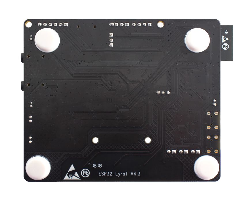
About This Document
The guidelines outline recommended design practices when developing standalone or add-on systems based on
the ESP32 series of products, including ESP32 SoCs, ESP32 modules and ESP32 development boards.

Document Updates
Please always refer to the latest version on https://www.espressif.com/en/support/download/documents.

Revision History
For the revision history of this document, please refer to the last page.

Documentation Change Notification
Espressif provides email notifications to keep customers updated on changes to technical documentation. Please
subscribe at www.espressif.com/en/subscribe. Note that you need to update your subscription to receive notifi-
cations of new products you are not currently subscribed to.

Certification
Download certificates for Espressif products from www.espressif.com/en/certificates.
Contents

1 Overview                                                                                               1

2 Schematic Checklist                                                                                    2
2.1    Power Supply                                                                                      3
      2.1.1 Digital Power Supply                                                                         3
      2.1.2 Analog Power Supply                                                                          4
2.2    Power-on Sequence and System Reset                                                                4
      2.2.1 Power-on Sequence                                                                            4
      2.2.2 Reset                                                                                        5
2.3    Flash (compulsory) and PSRAM (optional)                                                           5
2.4    Crystal Oscillator                                                                                6
      2.4.1 External Clock Source (compulsory)                                                           6
      2.4.2 RTC (optional)                                                                               7
2.5    RF                                                                                                8
2.6    ADC                                                                                               8
2.7    External Capacitor                                                                                9
2.8    UART                                                                                              9
2.9    SDIO                                                                                              10
2.10 Touch Sensor                                                                                        10

3 PCB Layout Design                                                                                      11
3.1    Standalone ESP32 Module                                                                           11
      3.1.1 General Principles of PCB Layout                                                             11
      3.1.2 Positioning an ESP32 Module on a Base Board                                                  12
      3.1.3 Power Supply                                                                                 13
      3.1.4 Crystal Oscillator                                                                           15
      3.1.5 RF                                                                                           16
      3.1.6 Flash & PSRAM                                                                                17
      3.1.7 External RC                                                                                  17
      3.1.8 UART                                                                                         17
      3.1.9 Touch Sensor                                                                                 18
3.2    ESP32 as a Slave Device                                                                           20
3.3    Typical Layout Problems and Solutions                                                             21
      3.3.1 Q: The current ripple is not large, but the TX performance of RF is rather poor.             21
      3.3.2   Q: The power ripple is small, but RF TX performance is poor.                               22
      3.3.3 Q: When ESP32 sends data packages, the power value is much higher or lower than the target
              power value, and the EVM is relatively poor.                                               22
      3.3.4 Q: TX performance is not bad, but the RX sensitivity is low.                                 22

4 Hardware Development                                                                                   23

5 Applications                                                                                           24
5.1    ESP32 Smart Audio Platform                                                                        24
5.1.1 ESP32-LyraT Audio Development Board         24
      5.1.2 ESP32-LyraTD-MSC Audio Development Board    25
5.2    ESP32 Touch Sensor Application—ESP32-Sense Kit   26
5.3    ESP-Mesh Application—ESP32-MeshKit               27

Revision History                                        28
List of Figures
 1    ESP32 Schematics (ESP32-D0WD used as an example for all illustrations in this section)   2
 2    ESP32 Digital Power Supply Pins                                                          3
 3    ESP32 Analog Power Supply Pins                                                           4
 4    Connections of ESP32 with Flash and PSRAM                                                6
 5    ESP32 Crystal Oscillator                                                                 6
 6    Schematic for ESP32’s External Crystal (RTC)                                             7
 7    Schematic of External Oscillator                                                         8
 8    ESP32 RF Matching Schematics                                                             8
 9    ESP32 External Capacitor                                                                 9
 10   ESP32 UART                                                                               9
 11   ESP32 PCB Layout                                                                         11
 12   ESP32 Module Antenna Position on Base Board                                              12
 13   Keepout Zone for ESP32 Module’s Antenna on the Base Board                                13
 14   ESP32 Power Traces in a Four-layer PCB Design                                            14
 15   Nine-Grid Design for EPAD                                                                14
 16   ESP32 Power Traces in a Two-layer PCB Design                                             15
 17   ESP32 Crystal Oscillator Layout                                                          16
 18   ESP32 RF Layout in a Four-layer PCB Design                                               17
 19   ESP32 RF Layout in a Two-layer PCB Design                                                17
 20   ESP32 Flash and PSRAM Layout                                                             18
 21   ESP32 UART Design                                                                        18
 22   A Typical Touch Sensor Application                                                       19
 23   Electrode Pattern Requirements                                                           19
 24   Sensor Track Routing Requirements                                                        20
 25   PAD/TV Box Layout                                                                        21
 26   Top View of ESP32-LyraT                                                                  24
 27   Bottom View of ESP32-LyraT                                                               25
 28   ESP32-LyraTD-MSC                                                                         26
 29   ESP32-Sense Kit                                                                          26
 30   ESP32-MeshKit-Light �                                                                    27
 31   ESP32-MeshKit-Sense Development Board                                                    27
1. OVERVIEW

1. Overview
ESP32 is a single 2.4 GHz Wi-Fi and Bluetooth combo chip designed with TSMC ultra-low-power 40 nm technol-
ogy. It is designed to achieve the best power and RF performance, robustness, versatility, and reliability in a wide
variety of applications and different power profiles.

ESP32 is a highly-integrated solution for Wi-Fi + Bluetooth applications in the IoT industry with around 20 external
components. ESP32 integrates the antenna switch, RF balun, power amplifier, low noise receive amplifier, filters,
and power management modules. As such, the entire solution occupies minimal Printed Circuit Board (PCB)
area.

ESP32 uses CMOS for single-chip fully-integrated radio and baseband, and also integrates advanced calibration
circuitries that allow the solution to dynamically adjust itself to remove external circuit imperfections or adjust to
changes in external conditions. As such, the mass production of ESP32 solutions does not require expensive and
specialized Wi-Fi test equipment.

The ESP32 series of chips includes ESP32-D0WD-V3, ESP32-D0WDQ6-V3, ESP32-D0WD(Not Recommended
For New Designs), ESP32-D0WDQ6(Not Recommended For New Designs), ESP32-S0WD, and ESP32-U4WDH,
among which, ESP32-D0WD-V3, ESP32-D0WDQ6-V3, and ESP32-U4WDH are based on ECO V3 wafer. For
details of part number and ordering information, please refer to ESP32 Series Datasheet. For details on ECO V3
instructions, please refer to ESP32 ECO V3 User Guide.

Espressif Systems                                         1                ESP32 Hardware Design Guidelines v3.2
                                           Submit Documentation Feedback
2. SCHEMATIC CHECKLIST
2. Schematic Checklist
ESP32’s integrated circuitry requires only 20 resistors, capacitors and inductors, one crystal and one SPI flash chip.
ESP32 integrates the complete transmit/receive RF functionality including antenna switches, RF balun, power am-
plifier, low noise receive amplifier, filters, power management module, and advanced calibration circuitries.
J1
1
ESP32’s high integration allows for simple
The peripheral of
capacitance circuit
C1 design.
and C2 This chapter details ESP32 schematics and
varies
with the selection of the crystal. CON1
PCB layout design. ESP32 schematic is shown in Figure 1. J4
1
GND CON1
J7
1
GND GND
4
3
U1
CON1
GND
GND XOUT
C1 C2 J10
TBD TBD 1
XIN
VDD33
CON1
1
2
C3 C20 J13
GND 1
100pF 1uF R1 20K(5%)
R2 GND
GND GND C5 C6 0R 40MHz+/-10ppm CON1
VDD33
GPIO21 J16
10nF/6.3V(10%) 3.3nF/6.3V(10%) R3 499R U0TXD 1
C9 U0RXD
GND GPIO22
0.1uF CON1
49
48
47
46
45
44
43
42
41
40
39
VDD33 GND J19
L5 2.0nH GND 1
GND
CAP1
CAP2
VDDA
XTAL_P
XTAL_N
VDDA
GPIO21
U0TXD
U0RXD
GPIO22
C13 C12 C11 C10 C21
C4 CON1
10uF NC 1uF 0.1uF NC VDD33 J22
0.1uF
GND VDD_SDIO 1
ANT1 GND GND GND GND
1 38 GPIO19
1 L4 TBD 2 VDDA GPIO19 37
2 3 LNA_IN VDD3P3_CPU 36 GPIO23 CON1
C15 C14 4 VDD3P3 GPIO23 35 GPIO18
C16 J25
VDD3P3 GPIO18
8
PCB ANT SENSOR_VP 5 34 GPIO5
TBD TBD 270pF(NC) 6 SENSOR_VP GPIO5 33 SDI/SD1 SCS/CMD 1 5 SDI/SD1 1
VCC
7 SENSOR_CAPP SD_DATA_1 32 SDO/SD0 /CS DI
270pF(NC) SENSOR_VN8 SENSOR_CAPN SD_DATA_0 31 SCK/CLK SCK/CLK 6 2 SDO/SD0
GND GND GND CHIP_PU 9 SENSOR_VN SD_CLK 30 SCS/CMD CLK DO CON1
GND
C17 GPIO34 10 CHIP_PU SD_CMD 29 SWP/SD3 SHD/SD2 7 3 SWP/SD3
VDET_1 SD_DATA_3 /HOLD /WP J28
GPIO35 11 28 SHD/SD2
GPIO32 12 VDET_2 SD_DATA_2 27 GPIO17 U3 FLASH 1
4
GPIO33 13 32K_XP GPIO17 26
VDD3P3_RTC
GPIO25 14 32K_XN VDD_SDIO 25 GPIO16
GPIO25 GPIO16 CON1
J31
GPIO26
GPIO27
C18 VDD_SDIO GND
GPIO2
GPIO0
GPIO4
MTMS
MTDO
MTCK
1
MTDI
1uF
U2 ESP32-D0WD CON1
J33
15
16
17
18
19
20
21
22
23
24
GND VDD33
1
C19 CON1
GPIO26
GPIO27
GPIO14
GPIO12
GPIO13
GPIO15
GPIO2
GPIO0
GPIO4
0.1uF J35
1
GND
CON1
Figure 1: ESP32 Schematics (ESP32-D0WD used as an example for all illustrations in this section) J37
1
CON1
Any basic ESP32 circuit design may be broken down into 10 major sections:
• Power supply
• Power-on sequence and system reset
• Flash and PSRAM (optional)
• Crystal oscillator
• RF
• ADC
• External capacitors
• UART
• SDIO
• Touch Sensor
Espressif Systems 2 ESP32 Hardware Design Guidelines v3.2
Submit Documentation Feedback
5 4 3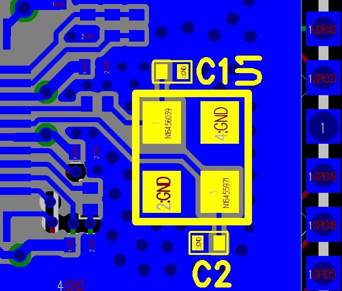
2. SCHEMATIC CHECKLIST
2.1 Power Supply
For further details of using the power supply pins, please refer to Section Power Scheme in ESP32 Series Datasheet.
2.1.1 Digital Power Supply
Pin19 and pin37 are the power supply pins for RTC and CPU, respectively. The digital power supply operates in
a voltage range of 1.8 V ~ 3.6 V. We recommend adding extra filter capacitors of 0.1 µF close to the digital power
supply pins. J1
1
The capacitance of C1 and C2 varies
VDD_SDIO (pin26)
withworks
theasselection
the power supply
of for
thethe crystal.
related IO, and also for an external device. CON1
J4
• When VDD_SDIO operates at 1.8 V, it can be generated from ESP32’s internal LDO. The maximum current 1
GND output voltage range is 1.65 V ~ 2.0 V. When the VDD_SDIO outputs
this LDO can offer is 40 mA, and the CON1
J7
1.8 V, the value of GPIO12 should be set to 1 when the chip boots and it is recommended that users add a 1
GND GND
4
3
2 kΩ ground resistor and a 4.7 µF filterU1capacitor close to VDD_SDIO.
CON1
GND
GND XOUT
C1 C2 J10
• When VDD_SDIO operates at 3.3 V, it is driven directly by VDD3P3_RTC through a 6 Ω resistor, therefore,
TBD TBD 1
XIN
there will be some voltage drop from VDD3P3_RTC. When the VDD_SDIO outputs 3.3 V, the value of GPIO12
CON1
1
2
J13
C3 is 0C20(default) when
GND
the chip boots and it is recommended that users add a 1 µF capacitor close to VDD_SDIO.
100pF 1uF 1
R1 20K(5%)
R2 GND
VDD_SDIO
GND GND
can also
C5 be C6
driven by an external power supply. The schematic for ESP32 digital power supply pins is
0R 40MHz+/-10ppm CON1
GPIO21 J16
10nF/6.3V(10%)
shown in Figure 2. 3.3nF/6.3V(10%) R3 499R U0TXD 1
C9 U0RXD
GND GPIO22
0.1uF CON1
49
48
47
46
45
44
43
42
41
40
39
GND J19
L5 2.0nH GND 1
GND
CAP1
CAP2
VDDA
XTAL_P
XTAL_N
VDDA
GPIO21
U0TXD
U0RXD
GPIO22
C12 C11 C10 C21
C4 CON1
NC 1uF 0.1uF NC VDD33 J22
0.1uF
GND VDD_SDIO 1
D GND GND GND
1 38 GPIO19
L4 TBD 2 VDDA GPIO19 37
3 LNA_IN VDD3P3_CPU 36 GPIO23 CON1
C15 C14 4 VDD3P3 GPIO23 35 GPIO18
C16 J25
SENSOR_VP 5 VDD3P3 GPIO18 34 GPIO5
8
TBD TBD 270pF(NC) 6 SENSOR_VP GPIO5 33 SDI/SD1 SCS/CMD 1 5 SDI/SD1 1
VCC
7 SENSOR_CAPP SD_DATA_1 32 SDO/SD0 /CS DI
270pF(NC) SENSOR_VN8 SENSOR_CAPN SD_DATA_0 31 SCK/CLK SCK/CLK 6 2 SDO/SD0
GND GND CHIP_PU 9 SENSOR_VN SD_CLK 30 SCS/CMD CLK DO CON1
GND
C17 GPIO34 10 CHIP_PU SD_CMD 29 SWP/SD3 SHD/SD2 7 3 SWP/SD3
VDET_1 SD_DATA_3 /HOLD /WP J28
GPIO35 11 28 SHD/SD2
GPIO32 12 VDET_2 SD_DATA_2 27 GPIO17 U3 FLASH 1
4
GPIO33 13 32K_XP GPIO17 26
VDD3P3_RTC
GPIO25 14 32K_XN VDD_SDIO 25 GPIO16
GPIO25 GPIO16 CON1
J31
GPIO26
GPIO27
C18 VDD_SDIO GND
GPIO2
GPIO0
GPIO4
MTMS
MTDO
MTCK
1
MTDI
1uF
U2 ESP32-D0WD CON1
J33
15
16
17
18
19
20
21
22
23
24
GND VDD33
1
C19 CON1
GPIO26
GPIO27
GPIO14
GPIO12
GPIO13
GPIO15
GPIO2
GPIO0
GPIO4
0.1uF J35
1
GND
CON1
Figure 2: ESP32 Digital Power Supply Pins J37
1
CON1
Notice: When using VDD_SDIO as the power supply pin for the external 3.3 V flash/PSRAM, the supply voltage should
be 3.0 V or above, so as to meet the requirements of flash/PSRAM’s working voltage.
Espressif Systems 3 ESP32 Hardware Design Guidelines v3.2
Submit Documentation Feedback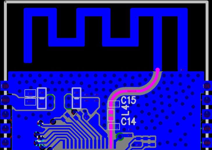
2. SCHEMATIC CHECKLIST
The capacitance of C1 and C2 v
with the selection of the crys
2.1.2 Analog Power Supply
Pin1, pin3, pin4, pin43 and pin46 are the analog power supply pins. It should be noted that the sudden increase
in current draw, when ESP32 is in transmission mode, may cause a power rail collapse. Therefore, it is highly
GND
recommended to add another 10 µF capacitor to the power trace, which can work in conjunction with the 0.1 µF
capacitor. LC filter circuit needs to be added near the power pin so as to suppress high-frequency harmonics.
GND GND
4
3
U1
The inductor’s rated current is preferably 500 mA and above.
GND
GND XOUT
The schematic for ESP32 analog power supply pins is shown in Figure 3. C1 C2
TBD TBD
XIN
VDD33
1
2
C3 C20
GND
100pF 1uF R1 20K(5%)
R2 GND
GND GND C5 C6 0R 40MHz+/-10ppm
VDD33
10nF/6.3V(10%) 3.3nF/6.3V(10%) R3 499R
C9
GND
0.1uF
49
48
47
46
45
44
43
42
41
40
39
VDD33 GND
L5 2.0nH
GND
CAP1
CAP2
VDDA
XTAL_P
VDDA
GPIO21
GPIO22
XTAL_N
U0TXD
U0RXD
C13 C12 C11 C10 C21
10uF NC 1uF 0.1uF NC
GND GND GND GND GND
ANT1 1
1 L4 TBD 2 VDDA GPIO19
2 3 LNA_IN VDD3P3_CPU
C15 C14 C16 4 VDD3P3 GPIO23
PCB ANT SENSOR_VP 5 VDD3P3 GPIO18
TBD TBD 270pF(NC) 6 SENSOR_VP GPIO5
7 SENSOR_CAPP SD_DATA_1
Figure 3: ESP32 AnalogSENSOR_VN
270pF(NC) Power Supply Pins
8 SENSOR_CAPN SD_DATA_0
GND GND GND CHIP_PU 9 SENSOR_VN SD_CLK
C17 GPIO34 10 CHIP_PU SD_CMD
GPIO35 11 VDET_1 SD_DATA_3
Notice: GPIO32 12 VDET_2 SD_DATA_2
GPIO33 13 32K_XP GPIO17
VDD3P3_RTC
• The recommended voltage of the power supply for ESP32 is 3.3 V, and
GPIO25 32K_XN
14 its recommended output current is 500 mA VDD_SDIO
GPIO25 GPIO16
or more.
GPIO26
GPIO27
GPIO2
GPIO0
GPIO4
MTMS
MTDO
MTCK
MTDI
• It is suggested that users add an ESD protection diode at the power entrance.
U2 ESP32-D0WD
15
16
17
18
19
20
21
22
23
24
2.2 Power-on Sequence and System Reset
GPIO26
GPIO27
GPIO14
GPIO12
GPIO13
GPIO15
2.2.1 Power-on Sequence
GPIO2
GPIO0
GPIO4
ESP32 uses a 3.3 V system power supply. The chip should be activated after the power rails have stabilized. This
is achieved by delaying the activation of CHIP_PU (Pin9) after the 3.3 V rails have been brought up. More details
can be found in Section Power Scheme in ESP32 Series Datasheet.
Espressif Systems 4 ESP32 Hardware Design Guidelines v3.2
Submit Documentation Feedback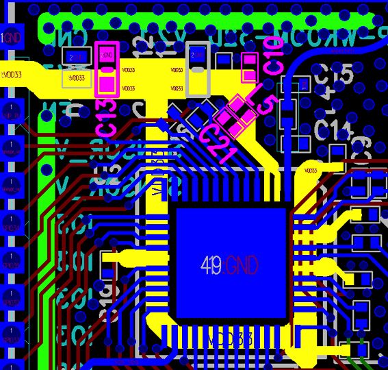
2. SCHEMATIC CHECKLIST

  Notice:
          To ensure the power supply to the ESP32 chip during power-up, it is advised to add an RC delay circuit at the
          CHIP_PU pin. The recommended setting for the RC delay circuit is usually R = 10 kΩ and C = 1 µF. However,
          specific parameters should be adjusted based on the power-up timing of the power supply and the power-up and
          reset sequence timing of the chip.

2.2.2 Reset
CHIP_PU serves as the reset pin of ESP32. The input level (VIL_nRST ) for resetting the chip should be low enough
and remain so for a period of time. More details can be found in Section Power Scheme in ESP32 Series Datasheet.
To avoid reboots caused by external interferences, the CHIP_PU trace should be as short as possible and routed
away from the clock lines. A pull-up resistor and a ground capacitor are highly recommended.

  Notice:
          CHIP_PU pin must not be left floating.

2.3 Flash (compulsory) and PSRAM (optional)
ESP32 can support up to 16 MB external flash and 8 MB external SRAM. The example module described in this
document uses a 4 MB flash by default (a SOP8 package, U3 on Figure 4). The VDD_SDIO acts as the power
supply pin. Make sure to select the appropriate flash according to the power voltage on VDD_SDIO.

  Note:

      • Some ESP32 chip variants (e.g. ESP32-U4WDH and ESP32-PICO) have flash already embedded in the chip
          package and adding external flash is not required. For details please see ESP32 and ESP32-PICO datasheets.

      • For the supported flash chips, see Section SPI Flash API in ESP-IDF Programming Guide.

On PSRAM, all pins except for the CS pin, can be multiplexed with flash. For example, PSRAM_CLK and
FLASH_CLK share the same SCK/CLK pin of ESP32 to use the pins efficiently, as shown in Figure 4. But in some
ESP32 module, such as ESP32-WROVER-E, flash has its own clock pin: SCK/CLK, and PSRAM uses GPIO17.
For more information, please see ESP32-WROVER-E Datasheet. The schematic of connections of ESP32 with
flash and PSRAM is shown in Figure 4. Note that the connection shown in Figure 4 is not the only way to connect
flash and PSRAM.

Espressif Systems                                           5                  ESP32 Hardware Design Guidelines v3.2
                                               Submit Documentation Feedback
499R(1%) U0TXD
U0RXD
GPIO22
2. SCHEMATIC CHECKLIST
ND
C4
VDD33
0.1uF/6.3V(10%)
SCK/CLK R17 0R(5%) FLASH_CLK
GPIO19
R16 0R(5%) SRAM_CLK
GPIO23
GPIO18 VDD_SDIO
GPIO5 VDD_SDIO
SDI/SD1
SDO/SD0
SCK/CLK
SCS/CMD R10
8
U3
SWP/SD3 10K(5%)
VDD33
SCS/CMD 1 5 SDI/SD1
VDD33
VCC
PCB ANT
VDD33
SHD/SD2 /CS DI U4
ANT1
GPIO17 FLASH_CLK 6 2 SDO/SD0 GPIO16 1 8
CLK DO SDO/SD0 2 CS# VDD 7 SHD/SD2
GND
GPIO16 SHD/SD2 7 3 SWP/SD3 SWP/SD3 3 SO/SIO1 SIO3 6 SRAM_CLK
VDD_SDIO /HOLD /WP 4 SIO2 SCLK 5 SDI/SD1
2
1
FLASH VSS SI/SIO0
10uF
4
C13
PSRAM (Optional)
GND GND
R4
GND GND GND GND
GND
2K(5%)(NC)
GND
C12
NC
TBD
VDD33
C15
L4
ND
C11
C19
1uF
0.1uF/6.3V(10%)
TBD
Figure 4: Connections of ESP32 with Flash and PSRAM
C14
ND
TBD
GND
0.1uF
C10
L5
100pF
C3
GND
C17
270pF(NC) SENSOR_VN8
270pF(NC)
C16
2.4 Crystal Oscillator
2.0nH
GND
GND
SCK/CLK R12 FLASH_CLK
clock0R(5%)
GND
There are two sources for the ESP32, that is, an external crystal oscillator clock source and an RTC clock
NC
C21
0.1uF
C9
1uF
C20
GPIO25
GPIO33
GPIO32
GPIO35
GPIO34
CHIP_PU
SENSOR_VP 5
source. R11
10nF/6.3V(10%)
0R(5%)(NC)
with the selection of the crystal.
The capacitance of C1 and C2 varies
0R(5%) SRAM_CLK
GPIO17
2.4.1 External
R13
Clock Source (compulsory)
GND
14
13
12
11
10
9
7
6
4
3
2
1
Currently, the ESP32 Wi-Fi/BT firmware only supports 40 MHz crystal oscillator. In circuit design, capacitors C1 and
C5
GND
GPIO25
32K_XN
32K_XP
VDET_2
VDET_1
CHIP_PU
SENSOR_VN
SENSOR_CAPN
SENSOR_CAPP
SENSOR_VP
VDD3P3
VDD3P3
LNA_IN
VDDA
C2 which connect to the ground are added to the input and output terminals of the crystal oscillator respectively.
49
The specific capacitive values
GNDdepend on further testing of, and adjustment to, the overall performance of the whole
3.3nF/6.3V(10%)
C6
R1
circuit. It is recommended that users reserve a series resistor of 0 Ω on the XTAL_P clock trace to reduce the drive
strength of the crystal, as well as to minimize the impact of crystal harmonics on RF performance. Note that the
20K(5%)
accuracy of the selected crystal is ±10 ppm. The schematic for crystal oscillator is shown in Figure 5.
48
CAP1 47
CAP2
TBD
46
C1
VDDA
GND
45
XTAL_P 44
0R 40MHz+/-10ppm
R2
RTC XTAL_N 43
VDDA
GND
42 1 4
GPIO21 41 XIN GND
U0TXD 40
U1
U0RXD
R3
39
GPIO22
GND
2 3
GND XOUT
VDD3P3_CPU
SD_DATA_2
SD_DATA_3
SD_DATA_0
SD_DATA_1
VDD_SDIO
499R
GND
SD_CMD
SD_CLK
GPIO16
GPIO17
GPIO18
GPIO23
GPIO19
GPIO5
TBD
C2
Figure 5: ESP32 Crystal Oscillator
25
26
27
28
29
30
31
32
33
34
35
36
37
38
0.1uF
C4
GND
Title
ESP32-W
GPIO16
GPIO17
SHD/SD2
SWP/SD3
SCS/CMD
SCK/CLK
SDO/SD0
SDI/SD1
GPIO5
GPIO18
GPIO23
GPIO19
GPIO22
U0RXD
U0TXD
GPIO21
Size Document Num
C
VDD33
Date: Wednesday, June
3Espressif Systems 6
2 ESP32 Hardware Design Guidelines v3.2
Submit Documentation Feedback
SHD/S
SCK/C
SCS/CIPEX: C15=2.2pF,L4=1.2nH,C14=3.0pF,R2=51R(5%)
GND
2. SCHEMATIC
PCB ANT: CHECKLIST
C15=2.4pF,L4=2.0nH,C14=3.3pF,R2=51R(5%)
4
3
GND U1 GND
GND
GND XOUT
Notice:
C1 C2
• If an oscillator is used, its output should be connected to XTAL_P on the chip through a DC blocking capacitor
XIN
VDD33 22pF/6.3V(10%) 22pF/6.3V(10%)
(about 10 pF). XTAL_N can be floating. Please make sure that the oscillator output is stable and its accuracy is
1
2
C3 C20
within ±10 ppm. The amplitude into XTAL_P can not exceed 1.1 V. It is also recommended that the circuit design
100pF/6.3V(10%) 1uF/10V(20%)
for the oscillator is compatible with the use of crystal, in case that if there is a defect in the circuit design,
R2
users can
VDD33 GND GND
GND GND R1 20K(5%) 51R(5%)
still use the crystal. 40MHz+/-10ppm
C9 C5 C6
• Defects in the craftsmanship of the crystal oscillators (for example, frequency deviation more than ±10 ppm) and R
0.1uF/6.3V(10%) 10nF/6.3V(10%) 3.3nF/6.3V(10%)
unstable operating temperature may lead to the malfunction of ESP32, resulting in a decrease of the overall per-
VDD33 GND GND
formance. L5 2.0nH(±0.1nH)
49
48
47
46
45
44
43
42
41
40
39
IPEX C12 C11 C10 C21 G
R14 0R(5%)/NC C13
1
GND
CAP1
CAP2
VDDA
XTAL_P
XTAL_N
VDDA
GPIO21
U0TXD
GPIO22
U0RXD
10uF/6.3V(10%) NC 1uF/10V(20%) 0.1uF/6.3V(10%) NC
J39
2
3
2.4.2
GND
RTC (optional)
GND GND GND GND GND
ANT1 1 38
R15 0R(5%) L4 VDDA GPIO19
ESP3212 supports an external 32.768 kHz 2.0nH(±0.1nH)
crystal or an external 32.768 kHz23 signal
LNA_IN(e.g., an oscillator) to act asVDD3P3_CPU
the 37
36
4 VDD3P3 GPIO23 35
C15 C14
RTC sleep clock.
PCB ANT SENSOR_VP 5 VDD3P3 GPIO18 34
2.4pF±0.25pF 3.3pF±0.25pF 6 SENSOR_VP GPIO5 33
7 SENSOR_CAPP SD_DATA_1 32
Figure 6 shows the schematic GND
for the external
GND
32.768 kHz crystal.
SENSOR_VN 8 SENSOR_CAPN SD_DATA_0 31
GND CHIP_PU 9 SENSOR_VN SD_CLK 30
GPIO34 10 CHIP_PU SD_CMD 29
GPIO35 11 VDET_1 SD_DATA_3 28
C17 TBD
GPIO32 12 VDET_2 SD_DATA_2 27
GND 32K_XP GPIO17
GPIO33 13 26
VDD3P3_RTC
GPIO25 14 32K_XN VDD_SDIO 25
GPIO25 GPIO16
R18
GPIO26
GPIO27
1
GPIO2
GPIO0
GPIO4
MTMS
MTDO
MTCK
MTDI
X1
32.768kHz
2
TBD U2 ESP32-D0WD
15
16
17
18
19
20
21
22
23
24
GND G
C18 TBD
GPIO26
GPIO27
GPIO14
GPIO12
GPIO13
GPIO15
GPIO2
GPIO0
GPIO4
Figure 6: Schematic for ESP32’s External Crystal (RTC) G
Notice:
• Please note the requirements for the 32.768 kHz crystal.
– Equivalent series resistance (ESR) ⩽ 70 kΩ.
– Load capacitance at both ends should be configured according to the crystal’s specification.
• The parallel resistor R18 is used for biasing the crystal circuit (5 MΩ < R18 ⩽ 10 MΩ).
• When ESP32-D0WD-V3 connects to an external 32.768 kHz crystal, the parallel resistor must be populated. For
other ESP32 series chips, the resistor can be reserved.
• If the RTC source is not required, then pin12 (32K_XP) and pin13 (32K_XN) can be used as GPIOs.
Figure 7 shows the schematic of the external signal.
The value of C1 should be larger than 200 pF. The signal should meet the following requirements:
32K_XN input Amplitude (Vpp, unit: V)
Sine wave or square wave 0.6 < Vpp < VDD
Espressif Systems 7 ESP32 Hardware Design Guidelines v3.2
Submit Documentation Feedback2. SCHEMATIC CHECKLIST
32K_XN
32768 kHz signal
ESP32
32K_XP
C1
Figure 7: Schematic of External Oscillator
2.5 RF
The output impedance of the RF pins of ESP32 (QFN 6*6) and ESP32 (QFN 5*5) are (30+j10) Ω and (35+j10) Ω,
respectively. A π-type matching network is essential for antenna matching in the circuit design. CLC structure is
recommended for the matching network. The schematic for ESP32 RF circuitry is shown in Figure 8.
ANT1 1
1 L4 TBD 2 VDDA
2 3 LNA_IN
C15 C14 4 VDD3P3
C16
SENSOR_VP 5 VDD3P3
PCB ANT
TBD TBD 270pF(NC) 6 SENSOR_VP
7 SENSOR_CAPP
270pF(NC) SENSOR_VN8 SENSOR_CAPN
GND GND GND CHIP_PU 9 SENSOR_VN
C17 GPIO34 10 CHIP_PU
11 VDET_1
Figure 8: ESP32 RF MatchingGPIO35
Schematics VDET_2
GPIO32 12
Note:
The parameters of the components in the matching network are subject to the actual antenna and PCB layout.
2.6 ADC
It is recommended that users add a 0.1 µF filter capacitor to a pad when using the ADC function.
• Pins SENSOR_VP or SENSOR_VN will trigger an input glitch lasting for 80 ns once SARADC1, or SARADC2,
or Hall sensor is initialized.
• Pins SENSOR_VP or SENSOR_VN is recommended for use as ADC.
• If SENSOR_VP and SENSOR_VN are used as GPIOs, while ADC is supported by other pins in the circuit
design, users need to do settings in software to avoid the input glitch.
• ADC1 is recommended over ADC2 as the latter cannot be used when Wi-Fi function is enabled.
• Currently, high-precision ADCs are not supported. The two 270 pF sampling resistors between SENSOR_VP
and SENSOR_CAPP, SENSOR_VN and SENSOR_CAPN, can be removed. In such case, the four pins can
be used as general ADCs or GPIOs.
Espressif Systems 8 ESP32 Hardware Design Guidelines v3.2
Submit Documentation Feedback2. SCHEMATIC CHECKLIST
• The recommended input voltage of the ADC is below 2450 mV, and preferably within the range of 100 to
950 mV for higher calibration accuracy. For details, please refer to Section ADC in ESP32 Series Datasheet.
2.7 External Capacitor
Figure 9 shows the schematic of components connected to pin47 CAP2 and pin48 CAP1. C5 (10 nF) that connects
to CAP1 should be of 10% tolerance and is required for proper operation of ESP32. RC circuit between CAP1
and CAP2 pins may be omitted under certain conditions. This circuit is used when entering Deep-sleep mode.
During this process, to minimize power consumption, the voltage to power ESP32 internals is dropped from 1.1
V to around 0.7 V. The RC circuit is used to minimize the period of the voltage drop. If removed, this process will
take longer and the power consumption in Deep-sleep will be higher. If particular application of ESP32 is not using
Deep-sleep mode, or power consumption is less critical, then this circuit is not required.
GND
R1 20K(5%)
C5 C6
10nF/6.3V(10%) 3.3nF/6.3V(10%)
GND
49
48
47
46
CAP1
CAP2
GND
VDDA
Figure 9: ESP32 External Capacitor
2.8 UART
Users need to connect a 499 Ω resistor to the U0TXD line in order to suppress the 80 MHz harmonics. The
schematic for ESP32 UART is shown in Figure 10.
R3 499R U0TXD
U0RXD
GPIO22
41
40
39
GPIO21
GPIO22
U0TXD
U0RXD
Figure 10: ESP32 UART
Espressif Systems 9 ESP32 Hardware Design Guidelines v3.2
Submit Documentation Feedback2. SCHEMATIC CHECKLIST
2.9 SDIO
There are two sets of GPIOs (slot0 and slot1) that can be assigned to SDIO on ESP32, as shown in the table below.
When ESP32 works as an SDIO host or slave, connect GPIOs in slot1 to signal lines.
CMD CLK DAT0 DAT1 DAT2 DAT3 Note
Used to connect flash by default. Not
Slot0 GPIO11 GPIO6 GPIO7 GPIO8 GPIO9 GPIO10
recommended for other use.
Multiplexed with JTAG, touch, EMAC,
Slot1 GPIO15 GPIO14 GPIO2 GPIO4 GPIO12 GPIO13
and strapping functions.
Note that when connecting GPIOs in slot1:
• When ESP32 works as SDIO host, add pull-up resistors on used pins, unused pins can be used for other
purposes.
• When ESP32 works as an SDIO slave, add pull-up resistors on all pins, whether these pins are used for SDIO
or not; unused pins cannot be used for other purposes.
For more information on SDIO configuration, please refer to API References.
2.10 Touch Sensor
When using the touch function, it is recommended to reserve a series resistor at the chip side to reduce the coupling
noise and interference on the line, and to strengthen the ESD protection. The recommended resistance is 470 Ω
~ 2 kΩ, preferably 510 Ω. The specific value also depends on the testing of the product.
Espressif Systems 10 ESP32 Hardware Design Guidelines v3.2
Submit Documentation Feedback3. PCB LAYOUT DESIGN
3. PCB Layout Design
This chapter introduces the key points of designing ESP32 PCB layout with the example of ESP32-WROOM-
32D.
While the high level of integration makes the PCB design and layout process simple, the performance of the system
strongly depends on system design aspects. To achieve the best overall system performance, please follow the
guidelines specified in this document for circuit design and PCB layout. All the common rules associated with
good PCB design still apply and this document is not an exhaustive list of good design practices.
The PCB layout design guidelines are applicable to cases when the
• ESP32 module functions as a standalone device, and when the
• ESP32 functions as a slave device.
The ESP32 PCB layout design is shown in Figure 11.
Figure 11: ESP32 PCB Layout
3.1 Standalone ESP32 Module
3.1.1 General Principles of PCB Layout
We recommend a four-layer PCB design.
• The first layer is the TOP layer for signal traces and components.
Espressif Systems 11 ESP32 Hardware Design Guidelines v3.2
Submit Documentation Feedback3. PCB LAYOUT DESIGN
• The second layer is the GND layer without signal traces being routed so as to ensure a complete GND plane.
• The third layer is the POWER layer where a GND plane should be applied to better isolate the RF and crystal
oscillator part. It is acceptable to route signal traces on this layer, provided that there is a complete GND
plane under the RF and crystal oscillator.
• The fourth layer is the BOTTOM layer, where power traces are routed. Placing any components on this layer
is not recommended.
Below are the suggestions for a two-layer PCB design.
• The first layer is the TOP layer for traces and components.
• The second layer is the BOTTOM layer. Please do not place any components on this layer and keep traces
to a minimum. Ideally, it should be a complete GND plane.
3.1.2 Positioning an ESP32 Module on a Base Board
If users adopt on-board design, they should pay attention to the layout of the module on the base board. The inter-
ference of the base board on the module’s antenna performance should be reduced as much as possible.
The module should be placed as close to the edge of the base board as possible. The PCB antenna area should
be placed outside the base board whenever possible. In addition, the feed point of the antenna should be closest
to the board, as Figure 12 shows.
If there is base board under the antenna area, it is recommended to cut it off to minimize its impact on the antenna.
When designing the whole device, pay attention to the impact of the device shell on the antenna. As shown in
Figure 12, positions 3 and 4 are highly recommended on the base board, while positions 1, 2, and 5 are not
recommended.
1 2 3 ✅
Base Board
5 4 ✅
Figure 12: ESP32 Module Antenna Position on Base Board
Espressif Systems 12 ESP32 Hardware Design Guidelines v3.2
Submit Documentation Feedback3. PCB LAYOUT DESIGN
If the positions recommended are not suitable, please make sure that the module is not covered by any metal
shell. The antenna area of the module and the area 15 mm outside the antenna should be kept clean, (namely no
copper, routing, components on it) as shown in Figure 13.
Clearance
15 mm
15 mm
15 mm
Base Board
Figure 13: Keepout Zone for ESP32 Module’s Antenna on the Base Board
3.1.3 Power Supply
• Four-layer PCB design
– Four-layer PCB design is recommended over two-layer design. Route the power traces on the fourth
(bottom) layer whenever possible. Vias are required for the power traces to go through the layers and
get connected to the pins on the top layer. There should be at least two vias where the main power
traces cross layers. The drill diameter on other power traces should be no smaller than the width of the
power traces.
– The 3.3 V power traces, highlighted in yellow, are routed as shown in Figure 14. The width of the main
power traces should be greater than 25 mil. The width of the power traces for pin3 and pin4 should be
at least 20 mil. The width of other power traces should be within the range of 12 ~ 15 mil.
– As shown in Figure 14, an ESD protection diode is placed close to the power port (marked in red circle).
A 10 µF capacitor is required before the power trace connects the ESP32 chip, to be used in conjunction
with a 0.1 µF capacitor. Then the power routing is divided into two ways. The power rails of pin3 and
pin4 should be routed together to reduce the coupling between different power pins.
– It is required to place C (capacitor) and L (inductor) near the power pins pin3 and pin4. As shown in
Figure 14, C13 (10 µF) is placed at the entrance of the power, and C10, L5, and C21 are placed near
the chip’s analog power pins. When possible, add a 0.1 µF capacitor to each digital power supply pin.
Note that all decoupling capacitors should be placed close to the power pin, and ground vias should
be added adjacent to the ground pin for the decoupling capacitors to ensure a short return path.
– The ground pad at the bottom of the chip should be connected to the ground plane through at least
nine ground vias.
Espressif Systems 13 ESP32 Hardware Design Guidelines v3.2
Submit Documentation Feedback3. PCB LAYOUT DESIGN
Note:
If you need to add a thermal pad EPAD under the chip on the bottom of the module, it is recommended to employ
a nine-grid on the EPAD, cover the gaps with ink, and place ground vias in the gaps, as shown in Figure 15. This
can avoid tin leakage when soldering the module EPAD to the substrate.
Figure 14: ESP32 Power Traces in a Four-layer PCB Design
Figure 15: Nine-Grid Design for EPAD
• Two-layer PCB design
In a two-layer PCB design, the 3.3 V power traces are routed as shown labelled with VDD33 in Figure 16.
In contrast to the design practices for a four-layer PCB design, the power traces in a two-layer PCB design
should be routed on the top layer, thus requiring a reduced size of a thermal pad in the center of the chip.
Route the power traces between the thermal pad and its surrounding signal pins. Employ vias only when the
Espressif Systems 14 ESP32 Hardware Design Guidelines v3.2
Submit Documentation Feedback3. PCB LAYOUT DESIGN
power traces have to reach the bottom layer. The purpose of this practice is to maintain a complete ground
plane while reducing the surrounding area of the power traces.
Other good practices for routing power traces in four-layer PCB designs still apply to two-layer PCB designs.
Figure 16: ESP32 Power Traces in a Two-layer PCB Design
3.1.4 Crystal Oscillator
For design of the crystal oscillator section, please refer to Figure 17. In addition, the following should be noted:
• The crystal oscillator should be placed far from the clock pin. The recommended gap is 2.7 mm. It is good
practice to add high-density ground via stitching around the clock trace for containing the high-frequency
clock signal.
• There should be no vias for the clock input and output traces, which means the traces cannot cross layers.
• When possible, the external regulating capacitor should be placed on the near left or right side of the crystal
oscillator, and at the end of the clock trace, to make sure the ground pad of the capacitor is close to that of
the crystal oscillator.
• Do not route high-frequency digital signal traces under the crystal oscillator. It is best not to route any signal
trace under the crystal oscillator. The vias on the power traces on both sides of the crystal clock trace
should be placed as far away from the clock trace as possible, and the two sides of the clock trace should
be surrounded by grounding copper.
• As the crystal oscillator is a sensitive component, do not place any magnetic components nearby that may
cause interference, for example large inductance component, and ensure that there is a clean large-area
ground plane around the crystal oscillator.
Espressif Systems 15 ESP32 Hardware Design Guidelines v3.2
Submit Documentation Feedback3. PCB LAYOUT DESIGN
Figure 17: ESP32 Crystal Oscillator Layout
3.1.5 RF
• Four-layer PCB design
In a four-layer PCB design, the RF trace is routed as shown highlighted in pink in Figure 18. The characteristic
RF impedance must be 50 Ω. The ground plane on the adjacent layer needs to be complete. Make sure to
keep the width of the RF trace consistent, and do not branch the trace. The RF trace should be as short as
possible with dense ground via stitching around it for isolation.
However, there should be no vias for the RF trace. The RF trace should be routed at a 135° angle, or with
circular arcs if trace bends are required.
π-type matching circuitry should be reserved on the RF trace and placed close to the chip.
No high-frequency signal traces should be routed close to the RF trace. The RF antenna should be placed
away from high-frequency transmitting devices, such as crystal oscillators, DDR, and clocks (SDIO_CLK),
etc.
In addition, the USB port, USB-to-UART chip, UART signal lines (including traces, vias, test points, header
pins, etc.) must be as far away from the antenna as possible. It is good practice to add ground vias around
the UART signal line.
• Two-layer PCB design
In a two-layer PCB design, the RF trace is routed as shown highlighted in pink in Figure 19. The width of the
RF trace should be greater than that of the RF trace in a four-layer board and is normally over 20 mil. The
actual width depends on the impedance formula where impedance-relevant parameters may vary depending
on the number of PCB layers.
Other good practices for routing RF traces in four-layer PCB designs still apply to two-layer board designs.
Espressif Systems 16 ESP32 Hardware Design Guidelines v3.2
Submit Documentation Feedback3. PCB LAYOUT DESIGN
Figure 18: ESP32 RF Layout in a Four-layer PCB Design
Figure 19: ESP32 RF Layout in a Two-layer PCB Design
3.1.6 Flash & PSRAM
Route the SPI traces of the flash and PSRAM on the inner layer (e.g., the third layer) whenever possible. Add
ground vias around the clock and data traces of SPI separately. The layout of the flash and PSRAM on ESP32 is
shown in Figure 20.
3.1.7 External RC
External resistors and capacitors should be placed close to the chip pins, and there should be no vias around the
traces. Please ensure that 10 nF capacitors are placed close to the pins.
3.1.8 UART
The series resistor on the U0TXD line needs to be placed as close to the chip and away from the crystal oscillator
as possible. Figure 21 below shows an example of UART design.
Espressif Systems 17 ESP32 Hardware Design Guidelines v3.2
Submit Documentation Feedback3. PCB LAYOUT DESIGN
Figure 20: ESP32 Flash and PSRAM Layout
Figure 21: ESP32 UART Design
3.1.9 Touch Sensor
ESP32 offers up to 10 capacitive IOs that detect changes in capacitance on touch sensors due to finger contact or
proximity. The chip’s internal capacitance detection circuit features low noise and high sensitivity. It allows users to
use touch pads with smaller area to implement the touch detection function. Users can also use the touch panel
array to detect a larger area or more test points. Figure 22 depicts a typical touch sensor application.
Espressif Systems 18 ESP32 Hardware Design Guidelines v3.2
Submit Documentation Feedback3. PCB LAYOUT DESIGN
Figure 22: A Typical Touch Sensor Application
In order to prevent capacitive coupling and other electrical interference to the sensitivity of the touch sensor system,
the following factors should be taken into account.
Electrode Pattern
The proper size and shape of an electrode improves system sensitivity. Round, oval, or shapes similar to a hu-
man fingertip is commonly applied. Large size or irregular shape might lead to incorrect responses from nearby
electrodes.
Figure 23: Electrode Pattern Requirements
Note:
The examples illustrated in Figure 23 are not of actual scale. It is suggested that users use a human fingertip as reference.
Espressif Systems 19 ESP32 Hardware Design Guidelines v3.2
Submit Documentation Feedback3. PCB LAYOUT DESIGN
PCB Layout
The following are general guidelines to routing traces:
• The trace length should not exceed 300 mm.
• The trace width (W) can not be larger than 0.18 mm (7 mil).
• The alignment angle (R) should not be less than 90°.
• The trace-to-ground gap (S) should be in the range of 0.5 mm to 1 mm
• The electrode diameter (D) should be in the range of 8 mm to 15 mm.
• Hatched ground should be added around the electrodes and traces.
• The traces should be isolated well and routed away from the antenna.
Figure 24: Sensor Track Routing Requirements
Note:
For more details on the hardware design of ESP32 touch sensor, please refer to ESP32 Touch Sensor Application Note.
3.2 ESP32 as a Slave Device
When ESP32 works as a slave device in a system, the user needs to pay more attention to signal integrity in the
PCB design. It is important to keep ESP32 away from the interferences caused by the complexity of the system
and an increased number of high-frequency signals. We use the mainboard of a PAD or TV Box as an example
here to provide guidelines for the PCB layout and design.
The digital signals between the CPU and DDR are the main producers of the high-frequency noise that interferes
with Wi-Fi radio. Therefore, the following should be noted with regards to the PCB design.
• As can be seen in Figure 25, ESP32 should be placed near the edge of the PCB and away from the CPU
and DDR, the main high-frequency noise sources. The distance between the chip and the noise sources
decreases the interference and reduces the coupled noise.
• It is suggested that a series resistor be reserved on the six signal traces when ESP32 communicates with
the CPU via SDIO to decrease the drive current and any interference, and also to eliminate the sequencing
problem caused by the inconsistent length of the SDIO traces.
Espressif Systems 20 ESP32 Hardware Design Guidelines v3.2
Submit Documentation Feedback3. PCB LAYOUT DESIGN
Figure 25: PAD/TV Box Layout
• On-board PCB antenna is not recommended, as it receives much interference and coupling noise, both of
which impact the RF performance. We suggest that you use an external antenna which should be directed
away from the PCB board via a cable, in order to weaken the high frequency interference with Wi-Fi.
• The high-frequency signal traces between the CPU and associated memory should be routed strictly ac-
cording to the routing guidelines (please refer to the DDR trace routing guidelines). We recommend that you
add ground vias around the CLK traces separately, and around the parallel data or address buses.
• The GND of the Wi-Fi circuit and that of other high-power devices should be separated and connected
through wires if there are high-power components, such as motors, in the design.
• The antenna should be kept away from high-frequency noise sources, such as LCD, HDMI, Camera Sensor,
USB, etc.
3.3 Typical Layout Problems and Solutions
3.3.1 Q: The current ripple is not large, but the TX performance of RF is rather poor.
Analysis:
The current ripple has a strong impact on the RF TX performance. It should be noted that the ripple must be
tested when ESP32 is in the normal working mode. The ripple increases when the power gets high in a different
mode.
Generally, the peak-to-peak value of the ripple should be3. PCB LAYOUT DESIGN
3.3.2 Q: The power ripple is small, but RF TX performance is poor.
Analysis:
The RF TX performance can be affected not only by power ripples, but also by the crystal oscillator itself. Poor
quality and big frequency offsets of the crystal oscillator decrease the RF TX performance. The crystal oscillator
clock may be corrupted by other interfering signals, such as high-speed output or input signals. In addition, high-
frequency signal traces, such as the SDIO trace and UART trace under the crystal oscillator, could also result in the
malfunction of the crystal oscillator. Besides, sensitive components or radiation components, such as inductors
and antennas, may also decrease the RF performance.
Solution:
This problem is caused by improper layout and can be solved by re-layout. Please see section 3 for details.
3.3.3 Q: When ESP32 sends data packages, the power value is much higher or lower
than the target power value, and the EVM is relatively poor.
Analysis:
The disparity between the tested value and the target value may be due to signal reflection caused by the impedance
mismatch on the transmission line connecting the RF pin and the antenna. Besides, the impedance mismatch will
affect the working state of the internal PA, making the PA prematurely access the saturated region in an abnormal
way. The EVM becomes poor as the signal distortion happens.
Solution:
Match the antenna’s impedance with the reserved π-type circuit on the RF trace, so that impedance of the antenna
as seen from the RF pin matches closely with that of the chip. This reduces reflections to the minimum.
3.3.4 Q: TX performance is not bad, but the RX sensitivity is low.
Analysis:
Good TX performance indicates proper RF impedance matching. External coupling to the antenna can affect the
RX performance. For instance, the crystal oscillator signal harmonics could couple to the antenna. If the TX and
RX traces of UART cross over with RF trace, then, they will affect the RX performance, as well. If ESP32 serves
as a slave device, there will be other high-frequency interference sources on the board, which may affect the Rx
performance.
Solution:
Keep the antenna away from crystal oscillators. Do not route high-frequency signal traces close to the RF trace.
High performance digital circuitry should be placed away from the RF block on large board designs. Please see
section 3 for details.
Espressif Systems 22 ESP32 Hardware Design Guidelines v3.2
Submit Documentation Feedback4. HARDWARE DEVELOPMENT
4. Hardware Development
Espressif designs and manufactures a large variety of modules and boards to help users evaluate functionality of
the ESP32 family of chips.
For a list of the latest versions of ESP32 modules and development boards, please refer to ESP32 Modules and
Boards.
To review module reference designs please check Documentation section of Espressif website.
Notes on Using Modules
• The module uses one single pin as the power supply pin. Users can connect the module to a 3.3 V power
supply. The 3.3 V power supply works both for the analog circuit and the digital circuit.
• The EN pin is used for enabling the chip. Set the EN pin high for normal working mode. There is no RC
delay circuit on the module. It is recommended that users add an external RC delay circuit to the module.
For details please refer to Section 2.2.
• Lead the GND, RXD, TXD pins out and connect them to a USB-to-UART tool for firmware download, log-
printing and communication.
By default, the initial firmware has already been downloaded in the flash. If users need to re-download the firmware,
they should follow the steps below:
1. Set the module to UART Download mode by pulling IO0 (pulled up by default) and IO2 (pulled down by
default) low. The chip IOs are pulled down internally by default.
2. Power on the module and check through the serial terminal if the UART Download mode is enabled.
3. Download the firmware to flash, using the Flash Download Tool.
4. After downloading, pull IO0 high or just leave it floating and use the internal weak pull-up to enable the SPI
Boot mode.
5. Power on the module again. The chip will read and execute the firmware during initialization.
Notice:
• During the whole process, users can check the status of the chip with the log printed through UART. If the firmware
cannot be downloaded or executed, users can check if the working mode is normal during the chip initialization by
looking at the log.
• The serial tool cannot be used for both the log-print and flash-download tools simultaneously.
Espressif Systems 23 ESP32 Hardware Design Guidelines v3.2
Submit Documentation Feedback5. APPLICATIONS
5. Applications
5.1 ESP32 Smart Audio Platform
5.1.1 ESP32-LyraT Audio Development Board
ESP32-LyraT is an open-source development board for Espressif Systems’ Audio Development Framework, ESP-ADF.
It is designed for smart speakers and smart-home applications. The dev board consists of the ESP32-WROVER/ESP32-
WROVER-B module, a Micro SD card, expansion interfaces, touch buttons and several function keys. It facilitates
the quick and easy development of dual-mode (Bluetooth + Wi-Fi) audio solutions , also supporting one-key
Wi-Fi configuration, a wake-up button, voice wake-up, voice recognition, cloud platform access, and an audio
player.
The ESP32-LyraT smart audio board has the following features:
• Various mainstream, both lossy and lossless, compressed audio formats, including M4A, AAC, FLAC, OGG,
OPUS, MP3, etc.
• One-key configuration and wake-up from the standby mode.
• SoftAP and Station mode.
• Various wireless protocols�Wi-Fi 802.11b/g/n, Classic BT and BLE.
• A series of audio inputs, including Wi-Fi, BT-audio, DLNA, Line-in, etc.
• BLE network configuration, and smart network configuration with apps, such as WeChat.
• Two microphones for the development of near-field and far-field voice recognition applications.
• Peripherals for differentiated demands.
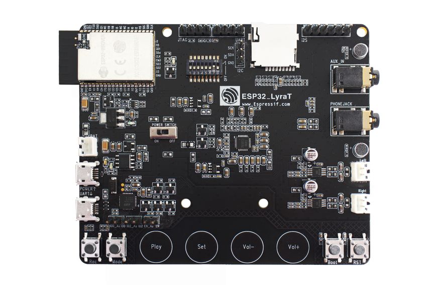
Figure 26 and 27 show the top view and bottom view of ESP32-LyraT.
Figure 26: Top View of ESP32-LyraT
Espressif Systems 24 ESP32 Hardware Design Guidelines v3.2
Submit Documentation Feedback5. APPLICATIONS
Figure 27: Bottom View of ESP32-LyraT
5.1.2 ESP32-LyraTD-MSC Audio Development Board
ESP32-LyraTD-MSC is designed for smart speakers and AI applications. This audio development board con-
sists of two parts: the upper board, which provides a three-microphone array, function keys and LED lights; and
the lower board, which integrates ESP32-WROVER-B, a MicroSemi Digital Signal Processing (DSP) chip, and
a power management module. ESP32-LyraTD-MSC facilitates the quick and easy development of dual-mode
(Bluetooth + Wi-Fi) audio solutions, as it supports one-key Wi-Fi network configuration, Acoustic Echo Cancel-
lation (AEC), near/far-field voice wake-up, cloud platform access, voice recognition, wake-up interrupt and audio
decoding.
The ESP32-LyraTD-MSC smart audio board has the following features:
• A lightweight, low-power and cost-effective smart audio solution.
• Access to multiple cloud platforms including DuerOS, Amazon, Tmall Genie, Turing, JD and iFLYTEK.
• HTTP live streaming, such as Internet radio and Ximalaya.
• Voice wake-up optimized with speech recognition and echo cancellation.
• Three digital MICs support far-field voice pick-up (from a distance of one to five meters).
• The dual-board design integrates an LED light strip and fully-functional buttons.
• Audio inputs over Wi-Fi, BT, DLNA, SD-Card.
• A variety of network configurations, such as Smartconfig, BLE, and Air-kiss.
• Wi-Fi 802.11b/g/n, Classic BT and BLE in the 2.4GHz band.
• Multiple audio formats including M4A, AAC, FLAC, OGG, OPUS, MP3, AMR.
ESP32-LyraTD-MSC’s layout is shown in Figure 28.
Espressif Systems 25 ESP32 Hardware Design Guidelines v3.2
Submit Documentation Feedback5. APPLICATIONS
Figure 28: ESP32-LyraTD-MSC
Note:
Espressif provides design guidelines for audio products based on ESP32. For details please refer to
ESP32 Audio Design Guidelines.
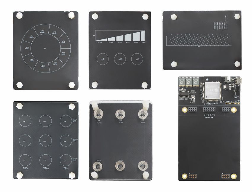
5.2 ESP32 Touch Sensor Application—ESP32-Sense Kit
The ESP32 touch sensor development kit, ESP32-Sense Kit, is used for evaluating and developing ESP32 touch
sensor system. ESP32-Sense Kit consists of one motherboard and multiple daughterboards. The motherboard
contains a display unit, a main control unit and a debug unit. The daughterboards have touch electrodes in different
combinations or shapes, such as linear slider, wheel slider, matrix buttons and spring buttons, depending on the
application scenarios. Users can design and add their own daughterboards for special usage cases.
The following image shows the whole ESP32-Sense development kit.
Figure 29: ESP32-Sense Kit
Espressif Systems 26 ESP32 Hardware Design Guidelines v3.2
Submit Documentation Feedback5. APPLICATIONS
5.3 ESP-Mesh Application—ESP32-MeshKit
ESP32-MeshKit is an all-in-one smart-light development kit, which is developed based on ESP-Mesh technology.
The development kit contains a number of ESP32-MeshKit-Lights and an ESP32-MeshKit-Sense board. ESP-
Mesh is developed upon ESP-MDF, Espressif Mesh Development Framework.
ESP32-MeshKit-Lights are smart lights besed on ESP-Mesh. Users can control the lights either with the ESP-Mesh
app, or the ESP32-MeshKit-Sense board that automatically switches on/off the lights by sensing the surrounding
temperature. ESP32-MeshKit-Lights also supports secondary development.
Figure 30 shows an ESP32-MeshKit-Light.
Figure 30: ESP32-MeshKit-Light �
ESP32-MeshKit-Sense is a development board with an ESP32 module at its core. It integrates a temperature and
humidity sensor and an ambient light sensor. The board can be connected to display screens. The integrated
sensors on the board can automatically switch on/off the ESP32-MeshKit-Lights by sensing the surrounding en-
vironment. Apart from smart lights, the development board can also form a mesh network with other devices.
In addition, the ESP32-MeshKit-Sense development board is a low-power sensing solution that can be used to
detect the current consumption of ESP32 modules in a normal operation state or in sleep mode, when connected
to different peripherals. Figure 31 shows an ESP32-MeshKit-Sense development board.
Figure 31: ESP32-MeshKit-Sense Development Board
Espressif Systems 27 ESP32 Hardware Design Guidelines v3.2
Submit Documentation FeedbackRevision History
Revision History
Date Version Release notes
Removed ESP32-D2WD chip variant from this document
Labelled ESP32-DOWD and ESP-D0WDQ6 chip variants as (Not Recommended
For New Designs)
2021-08-09 v3.2
Updated R4 to R18 in Figure 6
Added a note below Figure 2
Updated Section 2.3
2021-04-30 V3.1 Added a note in Section 2.3 Flash (compulsory) and PSRAM (optional)
Updated the C value of RC delay circuit in Section 2.2.1 from 0.1 µF to 1 µF
Added three chip variants ESP32-D0WD-V3, ESP32-D0WDQ6-V3, and ESP32-
U4WDH in Chapter 1
2020-09-25 V3.0 Added a note to EPAD in Chapter 3.1.3
Updated Chapter 2
Updated Chapter 4
Added documentation feedback link
Updated the note under Figure 12 about the recommended positions of ESP32 mod-
2019.10 V2.9
ules on the base board.
Changed the recommended minimum supply voltage of VDD_SDIO when powering
2019.09 V2.8
external 3.3 V flash/PSRAM to 3.0 V.
2019.04 V2.7 Updated Figure 6; added notes under the figure.
Added two-layer PCB design guidelines in Sections Power Supply and RF;
Updated Section UART;
2019.02 V2.6
Updated the modules supported on dev boards ESP32-LyraT and ESP32-LyraTD-
MSC according to the latest Espressif Product Ordering Information.
Updated Section Digital Power Supply: 2 kΩ resistor + 1 µF capacitor close to
2018.11 V2.5
VDD_SDIO when it outputs 1.8 V is changed to 2 kΩ resistor + 4.7 µF capacitor.
Updated Section 2.4.1: External Clock Source;
2018.09 V2.4
Updated Section 2.4.2: RTC.
2018.08 V2.3 Updated Section 2.7: External Capacitor.
Changed the official name of ESP-WROOM-32 into ESP32-WROOM-32;
Changed the official name of ESP-WROOM-32D into ESP32-WROOM-32D.
2018.07 V2.2
Updated Chapter 2: Schematic Checklist and PCB Layout Design;
Added new modules and applications based on ESP32.
Deleted sections introducing protocols, applications, block diagram and pin descrip-
tion of ESP32, for information of which please refer to ESP32 Series Datasheet;
Updated all figures and description of schematics and PCB layout in Chapter 2 ;
Added Section 2.6 ADC and 2.8 UART;
Updated Section 3, and added description about Positioning a ESP32 Module on a
Base Board in it.
2018.03 V2.1 Updated the value of current ripple in Section 3.3.1.
Updated Section ESP32-DevKitC Development Board.
Added Section ESP32-PICO-D4 Module.
Espressif Systems 28 ESP32 Hardware Design Guidelines v3.2
Submit Documentation FeedbackRevision History
Date Version Release notes
Added Section ESP32-WROOM-32D Module.
Added Section ESP32-WROOM-32U Module.
Added Section ESP32-PICO-KIT Mini Development Kit.
Deleted orginal Section 2.1.6 ESP32-PICO-KIT Mini Development Kit.
Changed the transmitting power to +12 dBm; the sensitivity of NZIF receiver to -97
dBm in Section Bluetooth;
Added a note to Table Pin Description;
2017.08 V2.0 Added Section 3.1.9 Touch Sensor;
Updated Chapter 4 Hardware Development;
Updated Section 5.1.1.
Changed the input power supply range of CPU/RTC IO to 1.8V ~ 3.6V;
2017.06 V1.9
Updated Section 2.1.1 Digital Power Supply.
Updated Section 2.2.1 Power-on Sequence;
Updated Section 2.4.1 External Clock Source (Compulsory);
2017.06 V1.8
Added a link to ESP32 Pin Lists;
Added Documentation Change Notification.
2017.05 V1.7 Added a note to Section ESP32-WROOM-32 Overview.
Updated Figure ESP32-WROOM-32 Pin Layout;
2017.05 V1.6
Added a note in Section Strapping Pins.
2017.04 V1.5 Added the ESP-WROOOM-32 module’s dimensional tolerance.
Updated Section Strapping Pins;
Updated Figure ESP32 Pin Layout (for QFN 5*5);
2017.04 V1.4
Updated Figure ESP32-WROOM-32 Module;
Updated Figure ESP32-DevKitC Pin Layout.
Updated the notice to Table ESP32 Pin Description;
2017.03 V1.3
Added a note to Table ESP32-WROOM-32 Pin Definitions.
Updated Chapter Overview;
Updated Figure Function Block Diagram;
Updated Chapter Pin Definitions;
Updated Section Power Supply;
2017.03 V1.2
Updated Section RF;
Updated Figure ESP32-WROOM-32 Pin Layout;
Updated Table ESP32-WROOM-32 Pin Definitions;
Updated Section Notes.
2016.12 V1.1 Updated Table UART to Wi-Fi Smart Device.
2016.12 V1.0 First release.
Espressif Systems 29 ESP32 Hardware Design Guidelines v3.2
Submit Documentation FeedbackDisclaimer and Copyright Notice
Information in this document, including URL references, is subject to change without notice.
ALL THIRD PARTY’S INFORMATION IN THIS DOCUMENT IS PROVIDED AS IS WITH NO
WARRANTIES TO ITS AUTHENTICITY AND ACCURACY.
NO WARRANTY IS PROVIDED TO THIS DOCUMENT FOR ITS MERCHANTABILITY, NON-
INFRINGEMENT, FITNESS FOR ANY PARTICULAR PURPOSE, NOR DOES ANY WARRANTY
OTHERWISE ARISING OUT OF ANY PROPOSAL, SPECIFICATION OR SAMPLE.
All liability, including liability for infringement of any proprietary rights, relating to use of information
in this document is disclaimed. No licenses express or implied, by estoppel or otherwise, to any
intellectual property rights are granted herein.
The Wi-Fi Alliance Member logo is a trademark of the Wi-Fi Alliance. The Bluetooth logo is a
registered trademark of Bluetooth SIG.
All trade names, trademarks and registered trademarks mentioned in this document are property
www.espressif.com of their respective owners, and are hereby acknowledged.
Copyright © 2021 Espressif Systems (Shanghai) Co., Ltd. All rights reserved.You can also read