Vision on Silicon Photonics for Efficient Data Communications - Maurizio Zuffada STMicroelectronics

Page created by Amanda Robertson
 
CONTINUE READING
Vision on Silicon Photonics for Efficient Data Communications - Maurizio Zuffada STMicroelectronics
Vision on Silicon Photonics
for Efficient Data Communications

             Maurizio Zuffada
           STMicroelectronics

       Photonics 21 - WG6 Workshop
          Brussels - April 30th, 2013
Vision on Silicon Photonics for Efficient Data Communications - Maurizio Zuffada STMicroelectronics
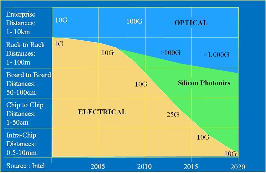
Outline       2

• Rationale

• Driving applications

• Silicon Photonics Today

• Key Technology Enablers

• Vision on Silicon Photonics: Road Map

• Conclusions
Vision on Silicon Photonics for Efficient Data Communications - Maurizio Zuffada STMicroelectronics
Rationale                                        3

• communications based on copper are approaching their intrinsic limits
• hybrid 2D-3D Photonics cannot meet the long term spec requirements
• Silicon Photonics can fill the gap
Vision on Silicon Photonics for Efficient Data Communications - Maurizio Zuffada STMicroelectronics
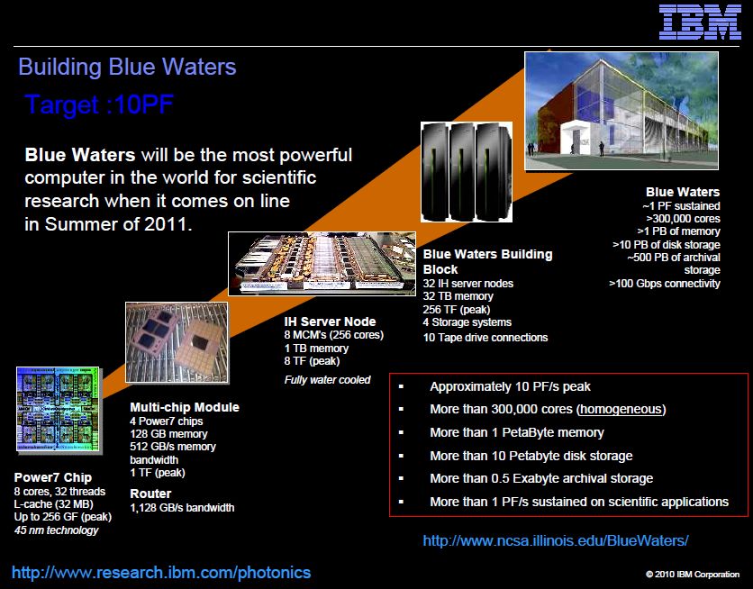
High Performance Computing                                         4

1000 EFLOPS

100 EFLOPS

    10 EFLOPS

     1 EFLOPS

100 PFLOPS

    10 PFLOPS

     1 PFLOPS

 100 TFLOPS

    10 TFLOPS

    1 TFLOPS

    100 GFLOPS

                 2000        2005             2010             2015             2020
•      flops increase 100% per year- Chip performance improves
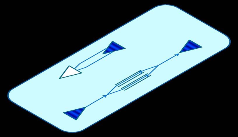
Vision on Silicon Photonics for Efficient Data Communications - Maurizio Zuffada STMicroelectronics
HPC Requirements                                             5

                2013           2016             2019              2022

  Flops          20 P         160 P            1.28 E            10.2 E

Aggregate      80 Pbps       640 Pbps       5.12 Ebps          40.8 Ebps
   BW

Energy/bit     75 pJ/bit     11 pJ/bit      1.7 pJ/bit          250 fJ/bit

             < 2400 mm3 /   < 120 mm3 /                        < 50 mm3 /
  Size
Vision on Silicon Photonics for Efficient Data Communications - Maurizio Zuffada STMicroelectronics
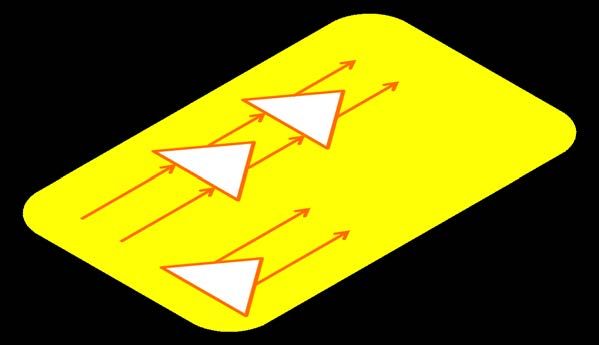
EO Transceiver & Optical Channel                                               6

            d1                           d2                            d1

        O        I   Electro   O                     I   Electro   O        I
 Chip                                                                           Chip
        /        /   Optical   /     Channel         /   Optical   /        /
  A     I        O             I                     O             I        O    B
                     Tx/Rx                               Tx/Rx
                        I                                   I

                     Lasers         o Aggregate BW        Lasers
                                    o Power/Energy
                                    o Size
                                    o Cost
Key assumptions:

• close proximity between Chip A/B and EO transceiver, i.e. d1 ≤ 10 cm
• channel based on SM Waveguides or Single Mode Fibers with d2 progressively scaling
  from cable lengths to intra-chip distances
• BER ≤ 10-12
Vision on Silicon Photonics for Efficient Data Communications - Maurizio Zuffada STMicroelectronics
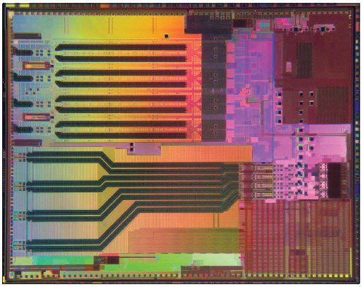
Silicon Photonics IC:
                                                                    7
      EO 40 Gbps Transceiver

 Rx-Buf.   Mach Zehnder Modulator

                                             I/O SM Fiber’s Array
                   Laser Input

                                    TIA-LA

 Tx-Buf.

Source : Luxtera
Vision on Silicon Photonics for Efficient Data Communications - Maurizio Zuffada STMicroelectronics
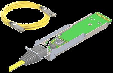
Silicon Photonics Layout                                                                  8

                                                                              CW Laser beam input

                                                            Grating Coupler

                                                          Beam Splitter

 Serial Data out
                                                                                                    Serial Data In

SM Fiber Input        SM Fiber Output

    Grating Coupler                     Grating Coupler
Silicon Photonics:
                                                       9
     Key Photonics Structures & Devices
• Grating Couplers for Input/Output Optical Coupling
   • Single Polarization Grating Coupler
   • Polarization Splitting Grating Coupler

• Single Mode & Multi Mode Wave Guides

• Beam Splitter

• WDM Mux/Demux

• Modulator

• Photodetector

• Laser
Key Technology Enablers                            10

• Separation of Photonics w Electronics

• Coarse Wave Division Multiplexing

• Laser Integration

• Low Cost EO Packages & EO PC Boards

• Energy & Size Efficient : Modulators, Filters & Switches

• Dense Wave Division Multiplexing

• Wafer-to-Wafer Molecular Bonding & Fluidic Cooling
Separation of Photonics - Electronics                                         11

• hybrid approach: Silicon Photonics IC Cu-Pillar Assy with Electronic IC

                                                    Mono-modal
                                                      Fiber

                                                                 Mono-modal
                                                                   Fiber

            CW LASER

        • pure Photonics IC : reduced number of masks  reduced cost
        • flexibility on electronics technology choice: CMOS/BiCMOS
        • DR up to 50G through Copper Pillars D=20 µm
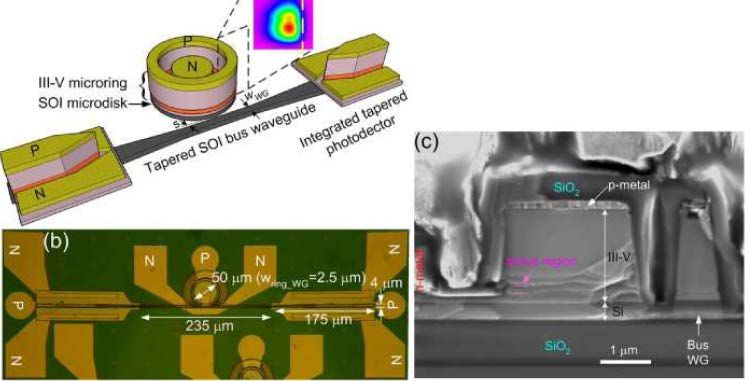
        • size effective : 3D assembly solution
Silicon Photonics: DFB Integrated Laser                                                           12

     Top view            III-V/Si active region                Si waveguide

       DBR                         N-                               Surface-grating
                                                                    coupler
                                 contact

                               P-contact           Mode transformer

                         Feed-back
          R>90%                                               R~50%
                                     InP                                         To fiber
                                                            Gain region
     Side view
                                Si waveguide

  Photonics Electronics Integration on CMOS: CEA-LETI, MINATEC Campus Grenoble (F) ESSCIRC 2011

                 advantages:
                    • cost reduction of the laser source (10 x)
                    • self alignment with no coupling losses
                    • multi-λ capability ( 4 λi lasers in 1 mm 2 )
From simple 3D to Full Photonics ASIC                                                                              13

             SiPho 3D                                Optical
                                          SiPho 3D
                                                     Coupling
       EIC
             OIC
                                    EIC
                                           OIC
       3D Silicon
         naked                     3D Silicon on                                                        Optical
                                                                                        SiPho 3D
                                     Package Classical Interposer                                       Coupling

                                                                                        EIC
                                                                       ASIC                     OIC

                                                                  3D Silicon Photonics Module on
                                                                          Classic Interposer
                                     Silicon Photonics
                                                                                              Optical
                                   Interposer with TSV
                                                                                              Coupling
                                                                ASIC            EIC

                                                      Optical Interposer with TSV and
  Silicon Photonics                                    separated Photonic Control IC
Interposer with TSV                                                                                    Optical
                                                     Optical                                          Coupling
                                                     Coupling
                    ASIC     EIP
                                                                                                      SiPho IC

          Optical Interposer with TSV and                                                SiPho + Interposer
       Photonic Control IP embedded into ASIC
200Gbps/link EO Transceiver
                     assembled on EO PCB                                    14

                                 Silicon_Photonics IC

2L BGA MB

5L EO PCB

1L WG EO PCB                           MIRROR

                                                                   2.5 mm
SUBSTRATE EO PCB                                        0

            •   close proximity with the Host IC
            •   aggregate full duplex BW = 50 G x 4 λ’s = 200 G/link
            •   estimated Power Consumption 600 mW/link
            •   estimated Module Size for 800 G in about 500 mm3
The MicroRing Resonator                                                15

                          Εin                 Εout A     1

          λ
    Q = −−−
         δλ                 Β0                Β
                                                         0
                                                                λm         λm-1   λ
                                         R
1
                                                                            2πR
          δλ                                           λm-1 − λm = neff    −−−−−−−−
                                                                          (m2 – m)
0                          Εout B
     λm        λm-1   λ

• the µ Ring resonators are very small structures typically with a R < 50 µm
• these structures are very good for: high speed modulators, filters and switches
• the µ Ring resonators are very sensitive to temperature variations (200ppm/°C)
Silicon Photonics: µ Ring Lasers                                                                   16

Electrically pumped compact hybrid silicon micro ring lasers for optical interconnects : 26 Oct. 2009
Vol.17 No.22 Optics Express

             advantages:
                • size reduction vs DFB Lasers ( 100 x)
                • low laser threshold current (10 mA)
Electronics-Photonics Integration                                                         17

   Silicon
   Photonics
    Wafer

   Electronic
     Wafer

  Photonics Electronics Integration on CMOS: CEA-LETI, MINATEC Campus Grenoble (F) ESSCIRC 2011

• silicon photonics wafer & elecronic wafer independently processed & finished
• low temperature wafer to wafer attachment through molecular bonding
• back-end finishing with vias and metals to connect Electronics and Photonics
2021 Opto Chip Assembly                                             18
1.6 mm

                                                                               Fluidic
                                                                               Cooling

                                     Heat Sink
                                                            Photonics layer
                                                             VLSI - IC
                                                                              Opto Chip
1 mm

                                                                              Assembled on
                                   Multi layer
                                   micro board                                EO Package
                                                 Lens

                     Multi layer
                     board
2 mm

         SM Polymeric Wave Guide                                               EO Board
                                                          Mirror

                                                        EO Board Substrate
Silicon Photonics Road Map                                                                         19

                                                                              Opto ASIC/ASSP
     Tech. Breakthrough                                                                            2 T/link
                                                                                                 6 mm2/link
                                                                                                  300 fJ/bit
                                                                                                  0.03 $/G
                                                                                                 DWDM + µR lasers
                                                Si_Photonics Interposers & Opto Board
                                                                 200 G/link
                                                                 6 mm2/link
                                                                   2 pJ/bit
                                                                 > 0.2 $/G
                                                                     CWDM & Lasers Integration

                                              Opto Modules & Opto Backplanes
                                  30G/link
                                 6mm2/link
                                  12 pJ/bit
                                   1 $/G

                                 Silicon Photonics Hybrid Approach
                                     Active Optical Cable
 10G/link
6mm2/link
 20 pJ/bit
  5 $/G
  2012       2013         2014         2015       2016         2017         2018       2019        2020
Conclusions                                            20

• Silicon Photonics is today in a niche market of the Active Optical Cables with
  limited volumes, nevertheless this technology has the potential to satisfy the
  future requirements of ICT & Consumer applications

• To enable high volume Silicon Photonics must improve the aggregate
  bandwidth/link by keeping the same size/link and by achieving :
   • Laser cost reduction through integration
   • Package cost reduction by satisfying the thermal constraints

• A vision of three consecutive Silicon Photonics generations can be seen for
  the next decade through which volume applications can grow consistently
  with the requirements of the future market
21

Thank you!
22

Back up
HPC Architectures   23
THE HPC & MODERN DATA CENTER
                                                                              24
            POWER ISSUE
• today Peta-Scale HPC & DATA CENTERS use an average between 40,000
  to 100,000 MCP with an average of 8 -16 cores for each processor

• the Bandwidth requirements scale, in average, roughly with 0.5B/FLOP 
  20 PFLOPS  BW = 80 ·106 Gb/s

• at the average of 75 mW/Gb/s  6 MW of power for data transfer + 6 MW
  of electrical power for cooling the system

• 2022 Exa-Scale HPC & DATA CENTERS will use an average of 70,000 MCP
  with an average of 128-256 cores for each processor

• the bandwidth requirements will scale at 40 ·109 Gb/s, but power for data
  transfer must be kept below 10 MW
Silicon Photonics 40 Gbps EO Transceiver                                                               25

Serial Data out                                                  Trans                        PSGC to
                                                 Limiter
     to                  Tx Buffer                             Impedance                      SM Fiber
                                                Amplifier
 VLSI Chip                                                      Amplifier                     Input

 CW
 Laser’s
 beam
 Input
                  SPGC                                                                       SPGC to
                          Splitter                                                           SM Fiber
                           by 2      Splitter                                                Output
                                                              MZ
                                      by 2                  Modulator

Serial Data in
                                                 CMOS                               TIA
  from                                                           Mod.       D.C.
                         Rx Buffer               Level                               &
 VLSI Chip                                                       Driver     Calib
                                                 Shifter                            Int.

  • a single laser source assembled in a µ-package (Popt < 13 dBm, Pel = 150 mW) split on 4 links
  • 4 Mach-Zehnder OOK modulated @ 10Gbps with thermal stabilization DC loop
  • 4 Modulators coupled to SM fiber’s array through 4 SPGC
  • 4 SM input fibers array coupled through 4 PSGC
Silicon Photonics 40Gbps EO Transceiver
                                                                      26
      Assembled in a QSFP Module for AOC
• single chip Silicon Photonics QSFP compatible

• QSFP module size: 10,000 mm3

• 40 Gb/s AOC up to 4 km w BER
The Side Coupled Integrated Spaced Sequence
 of Optical Resonators: SCISSOR                                                      27

         Εin                                                           Εout A

         Εout B
                  1

                  0
                       1500            1530                  λ [ nm]
                  1

                  0
                       1500            1530                  λ [ nm]

• the usage of µ Ring allows to integrate efficient modulators, filters & switches
You can also read