AN4022 Application note - TVS short pulse dynamic resistance measurement and correlation with TVS clamping voltage during ESD
←
→
Page content transcription
If your browser does not render page correctly, please read the page content below
AN4022
Application note
TVS short pulse dynamic resistance measurement
and correlation with TVS clamping voltage during ESD
Introduction
This application note is addressed to technical engineers and designers to explain how
STMicroelectronics measure and specify dynamic resistance RD in protection devices.
This parameter can be conveniently and accurately used to calculate the remaining voltage
after a transient voltage suppressor or a filter including protection, especially for devices
dedicated to protect against very fast transient surges such as ESD.
Market environment
Mobile phones, computers and their peripherals are sensitive electronic products. Each of
these products has to be protected against electrostatic discharge using components able
to clamp the high voltages generated in transients defined by each standard level such as
IEC 61000-4-2. Knowing the clamping voltage level of transient voltage suppressors is a key
point in the protection definition during the circuit design to get reliable and robust products.
This application note describes
The clamping characteristic
Dynamic resistance and how to measure it
Predicted results versus measured results
TLP measurements
October 2013 DocID022589 Rev 2 1/15
www.st.com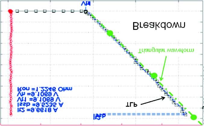
Clamping characteristic                                                                        AN4022

1          Clamping characteristic

           The remaining voltage across a TVS device is linked to its clamping characteristic. Figure 1
           shows the voltage across a unidirectional device versus the current flowing through it.

                     Figure 1. Typical clamping characteristic of a unidirectional device

                                              I

                                              IPP

                                                                                R
                                                                                 D

                                                    1 mA
                                Forward junction
                              V      area
                               CL

                                                                         VBR         VCL        V
                                                                      Breakdown area

                                    RD

                                                    IPP

2/15                                      DocID022589 Rev 2
AN4022                                                                        Clamping characteristic

         For a positive surge (Figure 2) the maximum voltage at the IC input is the clamping voltage
         VCL, directly linked to the VBR value of the device, and its dynamic resistance RD. For a
         negative surge (Figure 3) this remaining voltage is linked to its forward characteristic and its
         dynamic resistance RD.

                             Figure 2. Typical protection circuit, positive surge

                          Positive Surge

                                             I PP                                     IC
                                                                V CL
                                                                                      to
                                                                                   protect

                            Figure 3. Typical protection circuit, negative surge

                                                    I PP                                     IC
                                                                   V CL                      to
                                                                                      protect

                           Negative Surge

                                            DocID022589 Rev 2                                        3/15
                                                                                                            15
Clamping characteristic AN4022
The clamping characteristic of a bidirectional TVS is shown in Figure 4.
Figure 4. Typical clamping characteristic bidirectional device
I
IPP
RD
Breakdown area 1 mA
VCL VBR
VBR VCL V
1 mA Breakdown area
RD
IPP
Some TVS devices have a breakdown characteristic with a “snap-back” effect, allowing a
lower VBR value in one or both polarities, or a mix of the two characteristics (Figure 5).
Figure 5. Typical clamping characteristic of a “snap-back” TVS
I
I PP
RD
1 mA
Forward junction Snap-back effect
V CL
area
V BR V CL V
Breakdown area
RD
I PP
4/15 DocID022589 Rev 2AN4022 Dynamic resistance and how to measure it
2 Dynamic resistance and how to measure it
In the previous section it was shown that the remaining voltage across a circuit to protect is
closely linked to the VBR of the protection device used and to its dynamic resistance RD. The
first parameter is generally well known and specified. In the past dynamic resistance has
been specified but with test conditions different from real surge conditions giving pessimistic
results, especially for short surges like electrostatic discharges. The pulse used had a
duration of 2.5 µs.
To be closer to typical ESD (defined in IEC61000-4-2), a 100 ns pulse width has been
chosen.
An accurate voltage measurement is quite difficult during high rate of rise current, due to the
voltage probing loop inductance, inducing parasitic voltage:
().
VPARASITIC = LPARASITIC × dl/dt
So a triangular pulse is used This is shown in Figure 6. No oscillations disturb the
measurement.
Figure 6. Current and voltage waveforms for RD measurement
IPP = 30 A
VCL value
tP≈71 ns
The current is measured during the test by a current monitor (Pearson Electronics). The
voltage measurement is by the “Kelvin” method in coaxial configuration in order to get best
accuracy (test board shown in Figure 7). An adequate voltage range and offset is set on the
oscilloscope to get the best dynamic measurement without amplifier saturation.
DocID022589 Rev 2 5/15
15Dynamic resistance and how to measure it AN4022
Figure 7. Test board
The circuit can drive current from 500 mA up to 50 A, allowing measurements beyond the
IEC61000-4-2 standard highest level. In fact, at VPP = 15 kV contact, the current through the
device under test is 20 A to 62 A, between the first spike up to 60 ns. (Figure 8)
Figure 8. IEC61000-4-2 waveform, current level at VPP = 15 kV (contact discharge)
IPP = 62.3 A
IPP = 33.1 A
IPP = 19.2 A
To get the dynamic clamping characteristic of the device from 0 to IPP max, the current is
increase step by step, and at each level, the voltage is measured. Typical results up to
IPP = 40 A are shown in Figure 9. In this example, the device is an ESDA6V1P6.
6/15 DocID022589 Rev 2AN4022 Dynamic resistance and how to measure it
Figure 9. Dynamic clamping characteristic (unidirectional TVS)
IPP(A)
40
38
36
34
32
30
28
26
24 Breakdown
22 Forward
20
18 Linear (Breakdown)
16 Linear (Forward)
14
12
10
8
6
4
2 VCL(v)
0
0 5 10 15 20 25
y = 4.7921x -6.2303 y = 0.6765x -6.0637
R² = 0.9951 R² = 0.9976
The characteristic is linear in the interesting area and a good trend line can be extracted
(R2 = 0.99). A better representation can be obtained as in Figure 10, in order to calculate
directly the clamping voltage for a known IPP.
Figure 10. Clamping voltage VCL versus peak pulse current IPP
VCL(V)
20
18
16
14
12 Breakdown
Forward
10
Linear (Breakdown)
8 Linear (Forward)
6
4
2 IPP(A)
0
0 2 4 6 8 10 12 14 16 18 20 22 24 26 28 30 32 34 36 38 40
y = 0.2077 × + 1.3132 y = 0.3175 × + 6.9364
R² = 0.9951 R² = 0.9997
VCL = 0.2077 × IPP + 1.3132 VCL = 0.3175 × IPP + 6.9364
DocID022589 Rev 2 7/15
15Predicted results versus measured results AN4022
3 Predicted results versus measured results
With this information, we can now estimate the residual voltages remaining after the
protection device and compare these results with the results obtained during ESD surge
measurements. For this comparison the IEC61000-4-2 in contact mode has been selected.
In the standard, the current levels are specified versus the charging voltage (Figure 11).
Figure 11. Extract of IEC61000-4-2 standard [page 12], current levels versus charge
voltage levels (a)
From this table we can calculate the minimum and maximum current values that can be
found in our circuit, based on the tolerances specified (±15% or ±30% versus typical
values). The expected values are summarized in Table 1.
Table 1. Minimum, typical and maximum current values versus charge voltage
Level VPP (kV) Peak current (±15%) IPP@ 30 ns (±30%) IPP@ 60 ns (±30%)
1 2 6.37 7.5 8.62 2.8 4 5.2 1.4 2 2.6
2 4 12.75 15 17.25 5.6 8 10.4 2.8 4 5.2
3 6 19.12 22.5 25.87 8.4 12 15.6 4.2 6 7.8
4 8 25.5 30 34.5 11.2 16 20.8 5.6 8 10.4
a.STMicroelectronics thanks the International Electrotechnical Commission (IEC) for
permission to reproduce Information from its International Standard IEC 61000-4-2 ed.2.0
(2008).
All such extracts are copyright of IEC, Geneva, Switzerland. All rights reserved. Further
information on the IEC is available from www.iec.ch. IEC has no responsibility for the
placement and context in which the extracts and contents are reproduced by
STMicroelectronics, nor is IEC in any way responsible for the other content or accuracy
therein.
8/15 DocID022589 Rev 2AN4022 Predicted results versus measured results
The device under test is measured in ESD clamping test at the different standard voltage
levels, as in Figure 12 (example at +8 kV). The test conditions used are described in the
STMicroelectronics Application note AN3353, “IEC 61000-4-2 standard testing”.
Figure 12. Typical clamping voltage waveform with the measured values
t=30 ns t=60 ns
We get from these waveforms three values: the peak clamping voltage (first spike) and the
clamping voltages at t = 30 ns and t = 60 ns at peak charging voltage of ±2 kV, ±4 kV, ±6 kV
and ±8 kV. The values at the add point ±15 kV was also obtained, even if this point is not
specified in the standard.
We can now represent in three charts the predicted values and the real measurement
results in order to compare them.
Figure 13. Measurements and predicted values for the first spike peak value
VCL (V)
70
60 Breakdown
50
40 Predicted peak min
Predicted peak typical
30 Predicted peak max
Measured peak
20
10
VPP (kV)
0
0 2 4 6 8 10 12 14 16
DocID022589 Rev 2 9/15
15Predicted results versus measured results AN4022
Figure 14. Measurements and predicted values for 30 ns clamping value
V (V)
CL
20
18 Breakdown
16
14
12 Predicted 30 ns Min
Predicted 30 ns Typ
10
Predicted 30ns Max
8 Measured 30 ns
6
4 V (KV)
2 PP
0
0 2 4 6 8 10 12 14 16
Figure 15. Measurements and predicted values for 60 ns clamping value
V (V)
CL
20
18 Breakdown
16
14
12 Predicted 60 ns Min
Predicted 60 ns Typ
10
Predicted 60ns Max
8 Measured 60 ns
6
4 V (KV)
2 PP
0
0 2 4 6 8 10 12 14 16
Figure 13 shows the predicted results for the first spike voltage are far from the measured
values. In fact, the dl/dt during the first spike is very high, between 10 A/ns up to 80 A/ns
(the current rise time is around 0.75 ns). If we represent the V between the measured and
ΔV
the calculated dl/dt values versus the dl/dt, we get the curve in Figure 16. From this curve,
we can extract the value, shown in Figure 17. This value is near a constant, equal to the
parasitic inductance of the measurement loop (board, ground etc), in this case around
0.5 nH.
10/15 DocID022589 Rev 2AN4022 Predicted results versus measured results
Figure 16. Gap between measured and calculated values versus current rate of rise
ΔVCL(V)
50
40
30
20
10 dI/dt (A/ns)
0
0 20 40 60 80 100
Figure 17. Parasitic inductance
LPARASITIC(nH)
1.0
0.8
0.6
Average value: 0.5 nH
0.4
0.2 dI/dt (A/ns)
0.0
0 20 40 60 80 100
There are three considerations regarding the first spike:
This calculation of the VCL for this first spike is not correct for a bidirectional device or a
rail to rail plus Transil™ device (USBULC6-2F3 for example), because in this case, a
parameter called VFP linked to one of the junctions in forward conduction induces
another added spike voltage. This VFP depends on the diode technology and cannot be
easily evaluated.
We see here the importance of the parasitic inductances especially the ground
inductance return pass. The lower the value of this inductance, the lower the value of
this transient voltage.
This spike is not the most critical for the device to protect against because I/O’s IC
circuits are dimensioned to withstand short pulses with these levels, similar to machine
model ESD tests, for example.
From Figure 14 and Figure 15 we see the predicted values for the clamping voltages at
30 ns and 60 ns are very close to the measured results, assuming the dynamic
characteristic measured in these conditions are consistent, even at high current and voltage
levels.
Note: The study in forward polarity gives the same kind of results.
DocID022589 Rev 2 11/15
15TLP measurements AN4022
4 TLP measurements
A commonly used method to probe the dynamic characteristic of a TVS is the TLP
(transmission line pulse). This uses square pulses with a duration between 75 ns to 200 ns
with fast rise times of few nanoseconds. The equipment required is specific and expensive
and is dedicated to the characterization of the ESD robustness of protection devices,
especially for integrated circuit I/O’s. The equipment is usually limited to 10 A in maximum
current level (sometimes 20 A).
It is interesting to compare the results obtained by our method and the TLP method.
In Figure 18 and Figure 19, TLP measurements have been made on an ESDAULC6-1U2 up
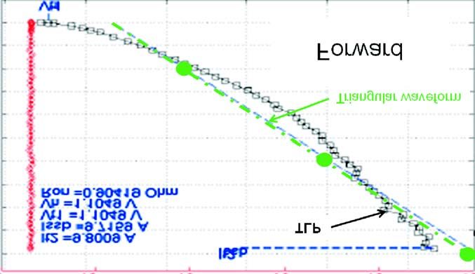
to 10 A, on the breakdown and forward area. The characteristics obtained by the triangular
pulse are superimposed in green. There is little difference between the two results.
Figure 18. TLP measurements compared with triangular waveform (breakdown
polarity)
Leakage current (A)
-12 -10 -8 -6 -4 -2
10 10 10 10 10 10
10 It2
It2 = 9.6618 A
9 Issb = 9.5235 A TLP
8 Vt1 = 9.1069 V
Vh = 9.1069 V
7
DUT current (A)
Ron = 1.2246 ohm
6
5
4 Triangular waveform
3
2 Breakdown
1
0
Vt1 DUT voltage (V)
0 5 10 15 20
12/15 DocID022589 Rev 2AN4022 TLP measurements
Figure 19. TLP measurements comparison with triangular waveform (forward
polarity)
Leakage current (A)
-12 -10 -8 -6 -4 -2
10 10 10 10 10 10
10 It2
It2 = 9.8009 A
9 Issb = 9.7159 A TLP
8 Vt1 = 1.1049 V
Vh = 1.1049 V
7
DUT current (A)
Ron = 0.90419 ohm
6
5
4
Triangular waveform
3
2
Forward
1
0 DUT voltage (V)
Vt1
0 2 4 6 8 10
Conclusion
To be sure a circuit design will be robust against electrostatic discharges, it is important to
anticipate the maximum voltage that can appear at the I/O’s of the sensitive circuits.
Knowing the dynamic characteristic of a transient voltage suppressor used for their
protection is a key point during the design.
We have shown in this note that this dynamic characteristic, measured with a short pulse,
not necessarily TLP, allows accurate prediction of the remaining voltage across the TVS,
especially after the first spike of a standard surge such as that defined in IEC61000-4-2,
where the circuit to protect is the most sensitive.
DocID022589 Rev 2 13/15
15Revision history AN4022
5 Revision history
Table 2. Document revision history
Date Revision Changes
20-Sep-2012 1 Initial release.
30-Oct-2013 2 Updated Figure 13.
14/15 DocID022589 Rev 2AN4022
Please Read Carefully:
Information in this document is provided solely in connection with ST products. STMicroelectronics NV and its subsidiaries (“ST”) reserve the
right to make changes, corrections, modifications or improvements, to this document, and the products and services described herein at any
time, without notice.
All ST products are sold pursuant to ST’s terms and conditions of sale.
Purchasers are solely responsible for the choice, selection and use of the ST products and services described herein, and ST assumes no
liability whatsoever relating to the choice, selection or use of the ST products and services described herein.
No license, express or implied, by estoppel or otherwise, to any intellectual property rights is granted under this document. If any part of this
document refers to any third party products or services it shall not be deemed a license grant by ST for the use of such third party products
or services, or any intellectual property contained therein or considered as a warranty covering the use in any manner whatsoever of such
third party products or services or any intellectual property contained therein.
UNLESS OTHERWISE SET FORTH IN ST’S TERMS AND CONDITIONS OF SALE ST DISCLAIMS ANY EXPRESS OR IMPLIED
WARRANTY WITH RESPECT TO THE USE AND/OR SALE OF ST PRODUCTS INCLUDING WITHOUT LIMITATION IMPLIED
WARRANTIES OF MERCHANTABILITY, FITNESS FOR A PARTICULAR PURPOSE (AND THEIR EQUIVALENTS UNDER THE LAWS
OF ANY JURISDICTION), OR INFRINGEMENT OF ANY PATENT, COPYRIGHT OR OTHER INTELLECTUAL PROPERTY RIGHT.
ST PRODUCTS ARE NOT DESIGNED OR AUTHORIZED FOR USE IN: (A) SAFETY CRITICAL APPLICATIONS SUCH AS LIFE
SUPPORTING, ACTIVE IMPLANTED DEVICES OR SYSTEMS WITH PRODUCT FUNCTIONAL SAFETY REQUIREMENTS; (B)
AERONAUTIC APPLICATIONS; (C) AUTOMOTIVE APPLICATIONS OR ENVIRONMENTS, AND/OR (D) AEROSPACE APPLICATIONS
OR ENVIRONMENTS. WHERE ST PRODUCTS ARE NOT DESIGNED FOR SUCH USE, THE PURCHASER SHALL USE PRODUCTS AT
PURCHASER’S SOLE RISK, EVEN IF ST HAS BEEN INFORMED IN WRITING OF SUCH USAGE, UNLESS A PRODUCT IS
EXPRESSLY DESIGNATED BY ST AS BEING INTENDED FOR “AUTOMOTIVE, AUTOMOTIVE SAFETY OR MEDICAL” INDUSTRY
DOMAINS ACCORDING TO ST PRODUCT DESIGN SPECIFICATIONS. PRODUCTS FORMALLY ESCC, QML OR JAN QUALIFIED ARE
DEEMED SUITABLE FOR USE IN AEROSPACE BY THE CORRESPONDING GOVERNMENTAL AGENCY.
Resale of ST products with provisions different from the statements and/or technical features set forth in this document shall immediately void
any warranty granted by ST for the ST product or service described herein and shall not create or extend in any manner whatsoever, any
liability of ST.
ST and the ST logo are trademarks or registered trademarks of ST in various countries.
Information in this document supersedes and replaces all information previously supplied.
The ST logo is a registered trademark of STMicroelectronics. All other names are the property of their respective owners.
© 2013 STMicroelectronics - All rights reserved
STMicroelectronics group of companies
Australia - Belgium - Brazil - Canada - China - Czech Republic - Finland - France - Germany - Hong Kong - India - Israel - Italy - Japan -
Malaysia - Malta - Morocco - Philippines - Singapore - Spain - Sweden - Switzerland - United Kingdom - United States of America
www.st.com
DocID022589 Rev 2 15/15
15You can also read