AURIX System Architecture - AURIX TC3xx Microcontroller Training V1.0 2020-06 - Infineon Technologies
←
→
Page content transcription
If your browser does not render page correctly, please read the page content below
AURIX™
System Architecture

AURIX™ TC3xx Microcontroller Training
V1.0 2020-06
               Please read the Important Notice and Warnings at the end of this document
AURIX™
System Architecture
Security & Memories: Highlights
Up to 6
Safety: RAM, Flash
SMU, HSM EEEPROM
TriCores › Multicore Microcontroller with embedded
Flash
Peripherals:
Timers: AURIX™ › TriCore™ (DSP processor) @300 MHz
DMA, ADC,
STM, GTP TC3xx GTM, CCU6
› Up to 16 MB Flash, more than 6 MB RAM
Communication Interfaces:
MCMCAN, Gigabit Ethernet MAC, SPI, UART, › DMA, HW-FFT, ADC, Gigabit Ethernet
I2C, ... MAC,...
Key Features Customer Benefits
Embedded flash platform for real time › Embedded flash allows compact design
applications and fast code execution
Up to 6 TriCore™ with DSP instructions › Enables heavy processing tasks like
radar or signal processing applications
Rich peripheral set and large RAMs › Reduces the need for external
components for cost competitive BOMs
2020-06-05 Copyright © Infineon Technologies AG 2020. All rights reserved. 2AURIX™
Embedded flash platform for real time applications
› All the flash memory is divided in banks (PF0-6 & DF0-1), which are concurrently readable.
› Each bank has it own Shared Resource Interconnect (SRI) ports, Error Correction Code
(ECC) decoders and pre-fetch logic.
› In case of ECC errors, the Safety Management Unit (SMU) and the Interrupt Router (IR) can
be configured to generate errors, respectively interrupts.
› This embedded flash platform offers a high performance code storage and flexible memory
selection, controlled by safety mechanisms.
Note: This is the general description of the Flash memory structure on AURIX™ TC3xx. This
depends on the device. Please refer to the according User Manual.
PF0 PF1 PF2 PFx DF/ROM/SFR
SRI Port SRI Port SRI Port SRI Port SRI Port
SMU ECC Err. ECC Err. ECC Err. ECC Err.
Buffer Buffer Buffer Buffer Command
PMU/Flash
Prefetch Prefetch Prefetch Prefetch Sequence
PMU0 Registers
Buffers Buffers Buffers Buffers Interpreter
IR
CCU ECC ECC ECC ECC
FSI
ECC ECC
DF1 Boot
PF0 PF1 PF2 PFx DF0
ROM
Program Flash Data Flash
2020-06-05 Copyright © Infineon Technologies AG 2020. All rights reserved. 3AURIX™
Up to 6 TriCore™ with DSP instructions
› The TriCore™ architecture combines three
powerful concepts:
CPU5
Checker Core
CPU4
– Microcontroller
CPU3
CPU2
CPU1
TC 1.6.2P
– RISC processor CPU0
– DSP (Digital Signal Processor)
› TC 1.6.2P:
– High performance architecture DFlash PFlash LMU DAM MCDS/
MINIMCDS
– Superscalar Harvard
– 6 pipeline stages for up to 300 MHz System Resource Interconnect
– 2.3 DMIPS/MHz
– Instruction and data cache SFI
EDS ADC
EDS ADC
DMA HSSL
Bridge
› 32bit Floating Point Unit in all CPUs: HSCT
HSM
MSC
SCU
FCE
IOM
Port
– Single precision according to IEEE-754
– 2 FLOPs per cycle (pipelined) System Peripheral Bus
MCM CAN
ETH MAC
ASC LIN
PSI5S
CCU6
ERAY
SENT
QSPI
GTM
PSI5
STM
GPT
I2C
AURIX™ TC39x Block Diagram
2020-06-05 Copyright © Infineon Technologies AG 2020. All rights reserved. 4AURIX™
Rich peripheral set and large RAMs
› Peripherals:
– ADC: Analog-Digital Convertor – 12-bit up to 1 MSPS
– GTM, GPT12 and CCU6: Signal Capture / Compare and PWM generation
– FFT engine: Fourier Transform acceleration
– STM: Timer Module
– DMA: Direct Memory Access Module
– Advanced On – Chip Debug System (OCDS)
› Communication Interfaces:
– QSPI: Advanced SPI interface (Serial Peripheral Interface)
– MCMCAN: CAN Interface
– ASCLIN: Lin and UART
– Gigabit Ethernet MAC: Ethernet 1000 Mbit/s interface
– I2C: Inter-Integrated Circuit Bus
– EBU: External Bus Unit (32-bit Data, 24-bit Address)
› On-Chip Memories:
– More than 6 MB integrated RAM including CPUs tightly coupled Scratch-Pad RAM
– Up to 16 MB integrated Flash memory with EEPROM Emulation
2020-06-05 Copyright © Infineon Technologies AG 2020. All rights reserved. 5AURIX™
Rich Peripheral set and large RAMs
AURIX™ Multi-CPU architecture
contains:
CPU5
Checker Core
CPU4
CPU3
CPU2
TC 1.6.2P
CPU1
› Distributed Scratch-Pad RAMs for data CPU0
(DSPR) and program (PSPR)
– Can be accessed by all CPUs DFlash PFlash LMU DAM MCDS/
MINIMCDS
› CPUs execute code from cached
System Resource Interconnect
PFlash modules
SFI
EDS ADC
EDS ADC
DMA HSSL
Bridge HSCT
HSM
MSC
SCU
FCE
IOM
Port System Peripheral Bus
MCM CAN
ETH MAC
ASC LIN
PSI5S
CCU6
ERAY
SENT
QSPI
GTM
PSI5
STM
GPT
I2C
AURIX™ TC39x Block Diagram
2020-06-05 Copyright © Infineon Technologies AG 2020. All rights reserved. 6AURIX™
System integration
› AURIX™ TC3xx combines three
powerful technologies within one
CPU5
Checker Core
CPU4
CPU3
CPU2
silicon die, improving power TC 1.6.2P
CPU1
CPU0
consumption, speed and reducing the
costs for embedded applications:
– Reduced Instruction Set Computing DFlash PFlash LMU DAM MCDS/
MINIMCDS
(RISC) processor architecture
System Resource Interconnect
– Digital Signal Processing (DSP)
operations and addressing modes SFI
EDS ADC
EDS ADC
DMA HSSL
Bridge HSCT
– On-chip memories and peripherals
HSM
MSC
SCU
FCE
IOM
Port
› AURIX™ TC3xx devices are designed
System Peripheral Bus
to meet the needs of embedded
control systems applications, where
MCM CAN
ETH MAC
ASC LIN
PSI5S
CCU6
ERAY
SENT
QSPI
GTM
PSI5
STM
GPT
I2C
real-time responsiveness,
computational power and data
bandwidth are key design elements AURIX™ TC39x Block Diagram
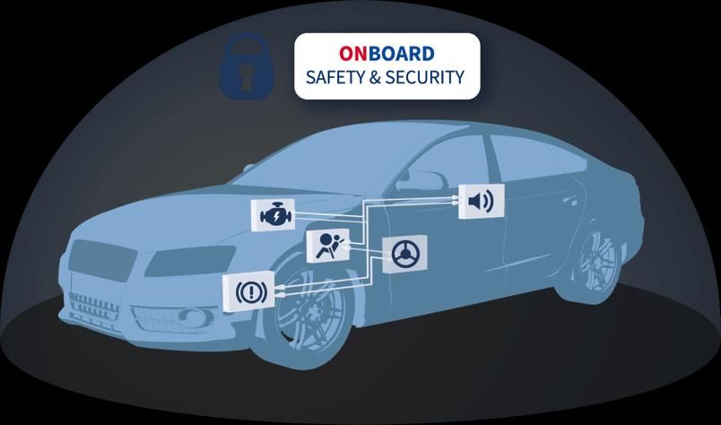
2020-06-05 Copyright © Infineon Technologies AG 2020. All rights reserved. 7Application Example
Automotive Industry
Overview
Car systems like airbag and engine
management need to operate in a safe and
secure way:
› Safe: Airbag must not trigger under
regular driving conditions
› Secure: Unauthorized persons must not
Engine Management Infotainment
be able to hack the car’s systems
Advantages Airbag Steering
Brake
Beside AURIX™ TC3xx versatile set of
on-chip peripherals connected to
TriCore™ CPUs, the AURIX™ family
also offers safety and security modules
to deal with critical embedded
applications.
2020-06-05 Copyright © Infineon Technologies AG 2020. All rights reserved. 8Trademarks
All referenced product or service names and trademarks are the property of their respective owners.
Edition 2020-06 IMPORTANT NOTICE For further information on the product,
Published by The information given in this document shall in no technology, delivery terms and conditions and
Infineon Technologies AG event be regarded as a guarantee of conditions or prices please contact your nearest Infineon
81726 Munich, Germany characteristics (“Beschaffenheitsgarantie”) . Technologies office (www.infineon.com).
With respect to any examples, hints or any typical
© 2020 Infineon Technologies AG. WARNINGS
values stated herein and/or any information
All Rights Reserved. Due to technical requirements products may
regarding the application of the product, Infineon
contain dangerous substances. For information
Technologies hereby disclaims any and all
Do you have a question about this on the types in question please contact your
warranties and liabilities of any kind, including
document? nearest Infineon Technologies office.
without limitation warranties of non-infringement
Email: erratum@infineon.com
of intellectual property rights of any third party. Except as otherwise explicitly approved by
Infineon Technologies in a written document
Document reference In addition, any information given in this
signed by authorized representatives of Infineon
AURIX_Training_2_System_Architecture document is subject to customer’s compliance
Technologies, Infineon Technologies’ products
with its obligations stated in this document and
may not be used in any applications where a
any applicable legal requirements, norms and
failure of the product or any consequences of the
standards concerning customer’s products and
use thereof can reasonably be expected to result
any use of the product of Infineon Technologies in
in personal injury.
customer’s applications.
The data contained in this document is exclusively
intended for technically trained staff. It is the
responsibility of customer’s technical
departments to evaluate the suitability of the
product for the intended application and the
completeness of the product information given in
this document with respect to such application.You can also read