BIS78 Pad and TDC status - Salvatore Loffredo, Dan Levin, Alexis Mulski, Riccardo Vari - CERN Indico
←
→
Page content transcription
If your browser does not render page correctly, please read the page content below
BIS78 Pad and TDC status

Salvatore Loffredo, Dan Levin, Alexis Mulski, Riccardo Vari

              RPC BIS78 DAQ and DCS meeting

                        17/12/2019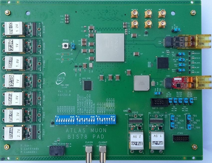
BIS78 Pad Board
                                                                                                                 The Pad board will be hosted in the
                                                                                                                 barrel region near to the BIS78
                                                                                                                 chambers (at most 6 m) and it will be
Salvatore Loffredo, Università degli studi di Roma Tor Vergata

                                                                                                                 used for the endcap trigger logic.
                                                                                                                 It will collect data from front-end
                                                                                                                 electronics, zero-suppress it and
                                                                                                                 send it to the off-detector Sector
                                                                                                                 Logic boards via optical fibers.
                                                                                                                 It is a prototype of the DCT board
                                                                                                                 (Data Collector and Transmitter) for
                                                                                                                 the ATLAS Phase II upgrade.

                                                                 BIS78 project is a fully representative pilot
                                                                 deployment of the new generation of RPC
                                                                 chambers and the ATLAS Phase II upgrade
                                                                 will benefit from this R&D activity.
                                                                  BIS78 Pad and TDC status       BIS78 DAQ and DCS meeting             17/12/2019    2/19
BIS78 PAD board in the TDAQ system

                                                                         BIS78 RPC
                                                                  ≈ 500 strip (eta and phi)                                                    Control
Salvatore Loffredo, Università degli studi di Roma Tor Vergata

                                                                                                                                                              ROD/ROS
                                                                                                                                                 PC

                                                                         Front-end                16 BIS78 stations
                                                                   ASD (Amplifier Shaper          1 Pad board and 18 HPTDC for
                                                                      Discriminator)              each station.                                                    FELIX
                                                                                                                         TTC, readout, init/control

                                                                                                                                                                      L1A
                                                                                              BC reset            BIS78 Pad board                              MuCTPi/
                                                                                              Clock (40MHz)                                                     CTP
                                                                   TDC and serializer                             GBT-
                                                                                                                            GBTx
                                                                      (18 HPTDC                                   SCA
                                                                                              JTAG
                                                                       18 GOL)                                                      Trigger
                                                                                              Serial out [18:1]                                                    Endcap
                                                                                              @ 1.6 Gb/s
                                                                                                                       FPGA         candidates Optical
                                                                                                                      Kintex-7                 splitter            sector
                                                                                                                                                                    logic
                                                                 Other signals from/to HPTDC board:
                                                                 TDC error[18:1], TDC reset,          On                 detector          Off detector
                                                                 GOL reset, 6 temperature analog signals
                                                                 (to the GBT-SCA).
                                                                    BIS78 Pad and TDC status              BIS78 DAQ and DCS meeting                   17/12/2019           3/19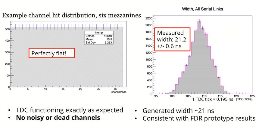
PAD logic board
The board hosts one FPGA (Xilinx Kintex 7 family), one GBTx chip and one
GBT-SCA chip.
The FPGA trigger algorithm perform a 2/3 majority logic (3 RPC gasgap) to
Salvatore Loffredo, Università degli studi di Roma Tor Vergata
select a muon candidate.
The board receives 18 serial data @ 1.6 Gb/s from HPTDC board.
Muon candidate information is sent to USA15 endcap sector logic board on
optical fiber.
GBTx serialize-de-serialize
data for timing, trigger, control GBT fibre to USA15 Felix
and readout; these data are (TTC, readout, init/control)
sent on a bidirectional optical
link. BC reset BIS78 Pad board
RPC readout data are stored in Clock (40MHz)
GBT-
FPGA and when a L1A signal is SCA
GBTx
detected, by means of GBTx, JTAG
they are sent through the Serial out [18:1] Optical out to USA15
FPGA (trigger candidates)
optical link to the Felix system. @ 1.6 Gb/s Kintex-7
Radiation tolerance certified.
Xilinx SEM core and triple
redundancy will be Signals from
HPTDC board
On detector Off detector
implemented.
BIS78 Pad and TDC status BIS78 DAQ and DCS meeting 17/12/2019 4/19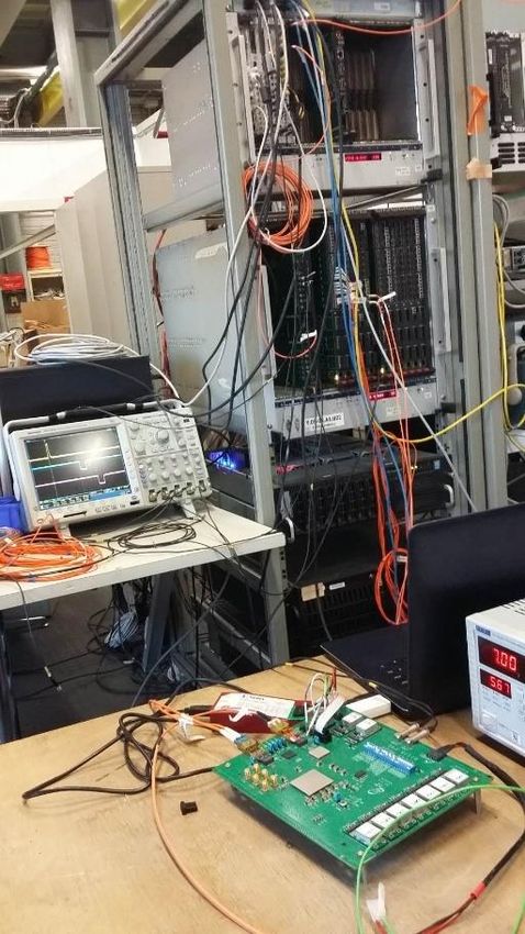
BIS78 PAD board
Board main components:
FPGA Kintex-7.
GBTx.
Salvatore Loffredo, Università degli studi di Roma Tor Vergata
GBT-SCA.
FMC connector for
HPTDC main board
(on the bottom side).
VTTx for trigger
output.
VTRx for Felix
readout and
control/monitoring.
9 FEAST voltage
regulators.
Flash memory
used to optionally
store the FPGA
configuration file.
JTAG connector is used for local FPGA /TDCs configuration (when GBT-SCA JTAG is not used).
GBTx I2C connector is used for local GBTx configuration.
Test points for active probe could be used to make clock signals characterization.
SMA connectors are for FPGA high speed serial link, lemo connectors for general purpose signals.
BIS78 Pad and TDC status BIS78 DAQ and DCS meeting 17/12/2019 5/19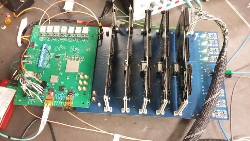
PAD integration test with Felix system
GBTx communication with Felix system is OK for all
the signals related to the EC field of the GBT-SCA;
Salvatore Loffredo, Università degli studi di Roma Tor Vergata
i.e. GBT-SCA JTAG, GPIO and ADC signals (such
as temperatures and power supplies).
The PAD board is able to receive and send data
back to the Felix system in GBT mode at 320 Mb/s
(8b/10b E-link encoding). In order to test the 80 bit
data field, we implemented an E-link loopback in
the FPGA. All 10 E-links are OK.
We tested an FPGA firmware in which PAD
receives data from 18 GOL outputs and read them
by means of Felix system in GBT mode at 320 Mb/s
rate with 8b/10b E-link Encoding on 9 different E-
links.
H[3:0] IC[1:0] EC[1:0] D[79:64] D[63:48] D[47:32] D[31:1 D[15: FEC[31:16] FEC[15:
6] 0] 0]
BIS78 Pad and TDC status BIS78 DAQ and DCS meeting 17/12/2019 6/19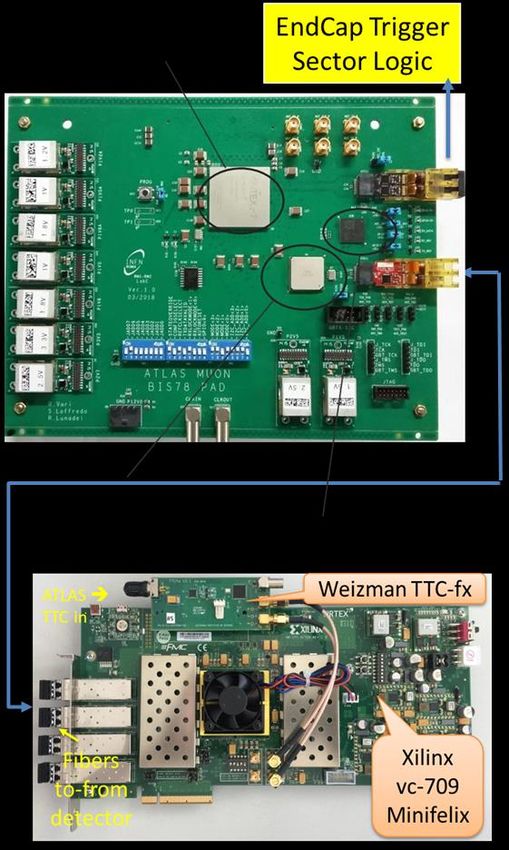
PAD integration test with endcap SL
Salvatore Loffredo, Università degli studi di Roma Tor Vergata

                                                                 -   A first test was done in October 2018 and
                                                                     then in June/July 2019 (results in backup slides).              Eye diagrams were taken;
                                                                 -   Additional tests have been made in November 2019, in            they have a 52.31 UI opening.
                                                                     which the path from the board to the SL was made by
                                                                     means of a 14 m fiber, a star module, a 46 m fiber and
                                                                     then the passive optical splitter 1 to 2 (ATLAS setup).
                                                                 -   IBERT test was done with data transfer rate of 6.4 Gb/s,
                                                                     31 bit PRBS Pattern.
                                                                 -   The board was always capable to send correctly the data
                                                                     and no error was found in more than 24 hours’ data taking.
                                                                     Bit error rate was less than 9.13E-16.
                                                                 -   We measured the latency associated to data transfer from
                                                                     PAD board to SL module (126 ns).
                                                                 -   The tests show that the latency is fixed after power cycling;
                                                                     we are using the transceiver configuration at fixed latency
                                                                     (no elastic buffer).
                                                                      BIS78 Pad and TDC status         BIS78 DAQ and DCS meeting                 17/12/2019     7/19
PAD integration test with HPTDC motherboard
All HPTDCs has been
correctly readout by means
of the FPGA.
Salvatore Loffredo, Università degli studi di Roma Tor Vergata
We tested an FPGA firmware
in which PAD receives data
from 18 HPTDCs and read
them by means of the Felix
system.
A preliminary integration test
with the RPC was made in
which we used the previous
firmware to readout a full
BIS7 RPC.
Significant improvements has been made in understanding the HPTDC and
detector data.
Motherboard clock signal is generated by GBTx and driven by FPGA.
HPTDC, GOL and BC reset signals are correctly driven by means of FPGA.
We are able to configure HPTDCs and to program the FPGA in the same GBT-SCA
JTAG chain; the maximum JTAG frequency is 10 MHz.
We are able to readout the temperature analog signals by means of the GBT-SCA.
The PAD power consumption with 18 FPGA High-Speed serial links enabled is
about 13 W.
BIS78 Pad and TDC status BIS78 DAQ and DCS meeting 17/12/2019 8/19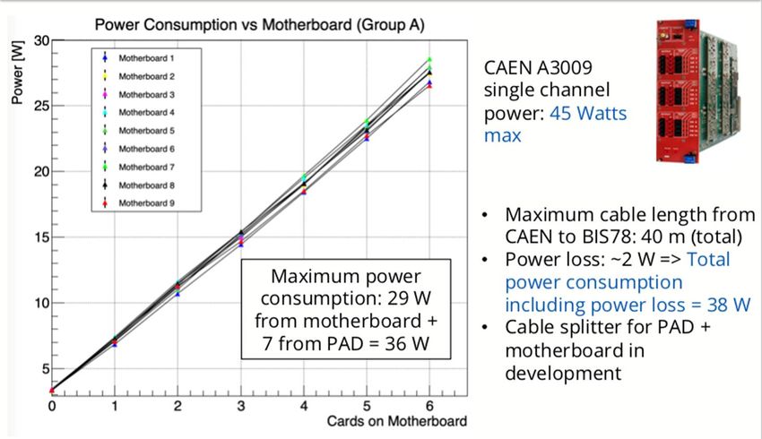
TDC status (1)
                                                                 Commissioning of Motherboards and Mezzanine Cards:

                                                                 10 Motherboards fabricated and delivered from China to BB5 in May 2019
Salvatore Loffredo, Università degli studi di Roma Tor Vergata

                                                                 54 Mezzanine cards fabricated and delivered from California to BB5 in May 2019

                                                                 Complete testing of these electronics: Alexis Mulski in summer 2019

                                                                   BIS78 Pad and TDC status     BIS78 DAQ and DCS meeting              17/12/2019   9/19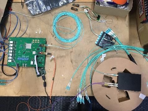
TDC status (2)
Salvatore Loffredo, Università degli studi di Roma Tor Vergata
Final result: All Mezz cards are fully tested and functional
All Motherboards fully tested and functional
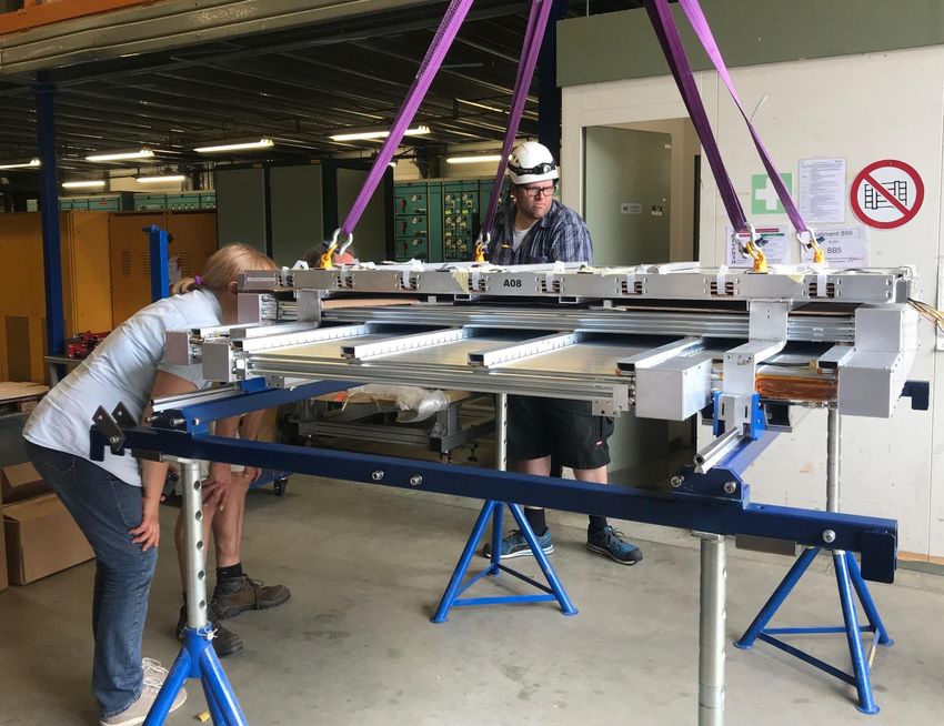
BIS78 Pad and TDC status BIS78 DAQ and DCS meeting 17/12/2019 10/19TDC integration test with RPC
Salvatore Loffredo, Università degli studi di Roma Tor Vergata
BIS78 Pad and TDC status BIS78 DAQ and DCS meeting 17/12/2019 11/19First test set up
Salvatore Loffredo, Università degli studi di Roma Tor Vergata
BIS78 Pad and TDC status BIS78 DAQ and DCS meeting 17/12/2019 12/19TDC efficiency
Salvatore Loffredo, Università degli studi di Roma Tor Vergata
Middle layer
efficiency = 93%
Result consistent with those
obtained using commercial Caen
in triggered mode
BIS78 Pad and TDC status BIS78 DAQ and DCS meeting 17/12/2019 13/19TDC resolution
Salvatore Loffredo, Università degli studi di Roma Tor Vergata
Arrival time difference
between hits on top and
middle layer
Result consistent with those
obtained using commercial Caen
in triggered mode
BIS78 Pad and TDC status BIS78 DAQ and DCS meeting 17/12/2019 14/19Second test setup
An FPGA preliminary firmware is done, in which PAD receives data from 18
HPTDCs and read them by means of Felix; this firmware has been tested reading
data from a full BIS7 chamber. Each HPTDC is connected to one different layer
Salvatore Loffredo, Università degli studi di Roma Tor Vergata
(top, middle, bottom) of the eta side and two HPTDCs are connected to one
different layer of the phi side (6 HPTDC).
The RPC layer connections are:
TDC1 -> top eta
TDC2 -> middle eta
TDC3 -> bottom eta
TDC4 -> top phi_1
TDC5 -> top phi_2
TDC6 -> middle phi_1
TDC7 -> middle phi_2
TDC8 -> bottom phi_1
TDC9 -> bottom phi_2
The RPC signals can be readout in triggerless and in auto-trigger mode; if auto-
trigger mode is used, it performs a 2/3 majority logic within a 100 ns time interval.
The trigger window is 1400 ns; the auto-trigger event is located at 400 ns within the
window.
When auto-trigger mode is used, only hits in the trigger window are written on disk;
hits belonging to the same window have the same event ID.
BIS78 Pad and TDC status BIS78 DAQ and DCS meeting 17/12/2019 15/19TDC power consumption
Salvatore Loffredo, Università degli studi di Roma Tor Vergata
TDC Power 28 W + cable loss 2 W + PAD 13 W = 41 W
BIS78 Pad and TDC status BIS78 DAQ and DCS meeting 17/12/2019 16/19Motherboard chassis and enclosures
5 4 3 2
DWG. NO.
4002517
ISSUE REVISIONS
CUSTOMER REQUEST
A 8-13-19 DAB
Salvatore Loffredo, Università degli studi di Roma Tor Vergata
1.800 B CUSTOMER REQUEST
A 1.772 REF. 8-14-19 DAB
45.7
.375 REF. 45 .250
REF. F
9.5 .500 .197 6.4
12.7 5
2
.500
12.7
.266 (2X)
A 6.8
8.100 REF. .984 .787
205.7 25 20
.394
10
OFFSET 1
"All sheets of this document contain
Z CLIP DETAILS proprietary and confidential information
of Bud Industries and is intended for E
.138 exclusive use by current Bud Industries
79.7 AUG 14 2019
personnel. Copying, disclosure to others, 3
or other use is prohibited without the
express written authorization of Bud
Industries."
B
.375 B
9.5 .922 PRINT APPROVAL
23.4 This print was checked by the undersigned.
( ) Disapproved - we made changes in red and signed them
( ) Approved as noted.
( ) Approved - we accept your dwg without correction and
1.800 will accept this part manufactured within the tolerances
45.7 indicated on this dwg. D
(Please check applicable statement above)
B
.201 (2X) Signed____________________
5.1
Date______________________
1.181 1.181
30 30
0
18.947
481.3
.837
21.3
9.105
231.3
.201 (5X)
5.1
BIS78 Pad and TDC status BIS78 DAQ and DCS
11.024 10.630meeting 17/12/2019 17/19C
280 270
19.435
493.7BCID
Salvatore Loffredo, Università degli studi di Roma Tor Vergata
Arrival time between successive events
generated at 9.8 KHz using reconstructed
BCID: recovered frequency is 9.8 KHz
BIS78 Pad and TDC status BIS78 DAQ and DCS meeting 17/12/2019 18/19Production and commissioning plans
TDC motherboard production:
Done
Salvatore Loffredo, Università degli studi di Roma Tor Vergata
PAD board production:
~ 2 months from date of purchase request
Manpower in 2020:
UM:
Dan Levin, Alexis Mulski, one student.
INFN:
Federico Lasagni, Salvatore Loffredo, Alessandro Polini, Marco Vanadia, Riccardo Vari.
Aim to test the electronics with its associated chamber before installation.
Installation schedule depends on NSW schedule.
BIS78 Pad and TDC status BIS78 DAQ and DCS meeting 17/12/2019 19/19Backup slides
Salvatore Loffredo, Università degli studi di Roma Tor Vergata
BIS78 Pad and TDC status BIS78 DAQ and DCS meeting 17/12/2019 20/19Bill of Material
Component Qty Manufacturer Use Radiation
name tolerance
certified
Salvatore Loffredo, Università degli studi di Roma Tor Vergata
GBTx 1 CERN Data serializer-de-serializer, FPGA and GBT- YES
SCA interface to VTRx
GBT-SCA 1 CERN Board local control (I2C, JTAG, general I/O) YES
VTTx 1 CERN Trigger data optical transmission YES
VTRx 1 CERN TTC, DCS and RPC data optical transmission YES
FEAST_CLP 9 CERN Voltage regulator YES
Kintex7 1 Xilinx Pad trigger logic YES
FPGA
EPROM 1 Micron FPGA configuration NO
Si545 2 Silicon labs FPGA and GBTx auxiliary reference clock NO
Kintex-7 FPGA (ordered) was tested against TID and SEE in 2018 by Rome group (NSW
Pad trigger board).
EPROM most probably not needed, FPGA will be programmed by means of Felix system.
Si545 has to be certified only for TID (no digital logic, no SEU events).
FEAST modules, VTTx, VTRx, GBTx, GBT-SCA: ordered at Cern and already delivered.
BIS78 Pad and TDC status BIS78 DAQ and DCS meeting 17/12/2019 21/19PAD board E-links
The board is able to support GBT, 8b/10b and wide bus mode.
It uses the 320 Mb/s E-link data rate, 2 E-links per group.
In the GBT mode, the up and down links are symmetrical within the GBT frame.
Salvatore Loffredo, Università degli studi di Roma Tor Vergata
Maximum number of Up/Down links in the 320 Mb/s GBT mode is 10 (higher for
the other modes).
GBT-SCA has a dedicated 80 Mb/s E-link (EC field).
The E-links related to the 80 bit data field are connected to the FPGA.
H[3:0] IC[1:0] EC[1:0] D[79:64] D[63:48] D[47:32] D[31:1 D[15: FEC[31:16] FEC[15:
6] 0] 0]
Frame Frame Frame Frame Frame
up/down up/down up/down up/down up/down
[111:96] [95:80] [79:64] [63:48] [47:32]
DIN[36,32] DIN[28,24] DIN[20,16] DIN[12,8] DIN[4,0]
DOUT[36,32] DOUT[28,24] DOUT[20,16] DIO[12,8] DIO[4,0]
BIS78 Pad and TDC status BIS78 DAQ and DCS meeting 17/12/2019 22/19PAD integration test with endcap SL (1)
Salvatore Loffredo, Università degli studi di Roma Tor Vergata
- A first test was done in October 2018.
- 40 MHz clock signals coming from TTC system for SL and
from Felix for PAD Board;
- GBTx takes care of generate and manage the 160 MHz
clock signal for the FPGA high-speed serial link connected
to VTTx;
- This link is used to send trigger data to the endcap Sector
Logic by means of fiber connection.
- IBERT test was done with data transfer rate of 6.4 Gb/s,
31 bit PRBS Pattern. No error observed, error rates are
less then 2.4E-14.
- Eye diagrams were taken using two different fiber length
(2.5 m and 30 m) with a 52.31 UI opening (worst case).
- We measured the latency associated to data transfer from
PAD board to SL module (126 ns).
BIS78 Pad and TDC status BIS78 DAQ and DCS meeting 17/12/2019 23/19PAD integration test with endcap SL (2)
Salvatore Loffredo, Università degli studi di Roma Tor Vergata
Other tests were done in June/July 2019.
BIS78 PAD to SL via optical splitter total lengths was
increased until 200 m using a fiber patch-panel.
- The 2 links (Pad 1 and Pad 2) used to send trigger data to the endcap Sector Logic
are buffered by means of 2 different passive optical splitters (1 to 2 and 1 to 4).
- IBERT test was done with data transfer rate of 6.4 Gb/s, 31 bit PRBS Pattern. Bit
errors were measured for about 24 hours, error rates are less then 1.8E-15 using the
optical splitter 1 to 2 (for VTTx output 1, 2) while splitter 1 to 4 shows worst values.
- No bit error was observed if the VTTx output 1 drives the 1-to-2 splitter (BER <
1.65E-15).
- Eye diagram was taken, it shows a UI values from 48 (splitter 1 to 4) to 58 (splitter 1
to 2); it is always opened widely.
- Current baseline for the fibers could be to
use 1 optical splitter 1 to 2 for each PAD, in
order to have 3 fibers from PAD to SL (1
direct + 2 from splitter).
Total fiber length 204 m, with the optical splitter 1 to 4
48.42 UI opening (worst case)
BIS78 Pad and TDC status BIS78 DAQ and DCS meeting 17/12/2019 24/1924 hours SL IBERT test result
Splitter 1 to 4 output PAD VTTx output Errors Bit error rate
Link 0 0 65 1.07E-13
Salvatore Loffredo, Università degli studi di Roma Tor Vergata
Link 1 0 3 4.95E-15
Link 2 0 20 3.30E-14
Link 3 0 7 1.16E-14
Link 0 1 3 5.46E-13
Link 1 1 0 < 1.80E-15
Link 2 1 0 < 1.80E-15
Link 3 1 0 < 1.80E-15
Splitter 1 to 2 output PAD VTTx output Errors Bit error rate
Link 0 0 0 < 1.80E-15
Link 1 0 1 1.80E-15
Link 0 1 0 < 1.65E-15
Link 1 1 0 < 1.65E-15
Splitter outputs driven by VTTx output 1 shows a lower bit error rate.
No bit error was observed if VTTx output 1 drives the 1-to-2 splitter.
Total fiber length 204 m.
BIS78 Pad and TDC status BIS78 DAQ and DCS meeting 17/12/2019 25/19You can also read


