CONDUCTION AND RESISTIVE SWITCHING MEMORY IN AL/MOS2+PVP/AG DEVICES FABRICATED USING DROP CAST METHOD
←
→
Page content transcription
If your browser does not render page correctly, please read the page content below
Conduction and Resistive Switching Memory in Al/MoS2+PVP/Ag Devices Fabricated using Drop cast Method Zolile Wiseman Dlamini ( 46118357@mylife.unisa.ac.za ) UNIVERSITY OF SOUTH AFRICA Sreedevi Vallabhapurapu University of South Africa Tebogo S so Mahule University of South Africa Shuying Wu Macquarie University Vijaya Srinivasu Vallabhapurapu University of South Africa Research Article Keywords: MoS2, PVP, Resistive switching, drop cast Posted Date: October 6th, 2021 DOI: https://doi.org/10.21203/rs.3.rs-956321/v1 License: This work is licensed under a Creative Commons Attribution 4.0 International License. Read Full License
Conduction and Resistive Switching Memory in Al/MoS2+PVP/Ag Devices Fabri-
cated using Drop cast Method
 Zolile Wiseman Dlamini1,2,*, Sreedevi Vallabhapurapu3, Tebogo Sfiso Mahule1, Shuying Wu4 and
 Vijaya Srinivasu Vallabhapurapu1

 1
 Department of Physics, University of South Africa, 28 Pioneer Ave, Florida Park, 1709, Gauteng, South Af-
 rica
 2
 Department of Maths, Science and Technology Education, Central University of Technology, 20 President
 Brand St., Bloemfontein, 9300, Free State, South Africa.
 3
 School of Computing, University of South Africa, 28 Pioneer Ave, Florida Park, 1709, Gauteng, South Af-
 rica.
 4
 School of Engineering, Macquarie University, Balaclava Road, Macquarie Park NSW, 2109, Sydney, Aus-
 tralia.

 *
 Corresponding author. E-Mail: zoliledlamini@hotmail.com

 Abstract. Resistive switching in MoS2 embedded PVP composite-based ReRAM with Al and Ag electrodes is
reported. A cost-free drop cast method was used to deposit active layers consisting of 30 wt%, 40 wt%, and 70
wt% of MoS2 in PVP. Each system exhibited unique electroforming and switching mode. Asymmetrical bipolar
resistive switching occurring only in the positive voltage bias, a typical bipolar resistive switching and a typical
‘O-type’ resistive switching were observed for the 30 wt%, 40 wt%, and 70 wt% systems, respectively. Further-
more, injection of charge carriers at the electrode/active layer interface and electrochemical metalization
mechanisms drove the formation of a nanoscale conductive filament in the device A and B. On the other hand,
we attributed the conduction mechanism of device C to hopping conduction. Our results demonstrate the be-
haviour of MoS2 embedded PVP composite-based ReRAM has a strong dependence on the amount of MoS2
and that both the switching and conduction mechanism can be exploited by controlling the amount of MoS2 in
the composite.

 Keywords: MoS2, PVP, Resistive switching, drop cast

1 Introduction
 Research efforts are put towards developing biodegradable electronics devices to reduce
environmental pollution and toxins caused by the disposal of current electronic devices. The
memory device industry also develops next-generation resistive switching memory (ReRAM)
using biodegradable materials[1–5]. ReRAM uses a dielectric material called an active layer
sandwiched between two electrodes. Each ReRAM cell has two distinctive resistive states,
i.e., a high resistive state (HRS) and a low resistive state (LRS), which are selectable using
electric stimuli[6]. Since their discovery[7], ReRAMs have shown good properties such as mi-
nuscule cell size (< 10 ), long retention time (> 106 ), high operating speed ( − ),
multilevel data storage capability, good endurance, large ON/OFF ratio and many more[3–
5], making them a potential replacement of the current memory giants, i.e., dynamic random
access memory (DRAM) and Flash memory. Current memory devices seem to not comply
with the projected Si-Logic level of up to 0.1 operating voltage[8]. Poly(vinylpyrroli-
done)(PVP) is a water-soluble and nontoxic synthetic polymer permitted for use in the
cosmetics, food, and drug industries[9]. PVP blended with other polymers, such as poly-
acrylamide[10], and other complexes such as KIO4[11] have demonstrated good electrical
properties in thin-film samples. PVP has also shown strong interaction with metal cations[12],
making it possible to tailor its electronic properties for various applications such as batter-
ies[13]. PVP dispersed with MoS2 ReRAM systems have shown exciting memory behaviour.
Bai et al. [14] observed three switching modes, i.e., bipolar, asymmetric bipolar and thresh-
old switching(TS) in the same system of PVP and MoS2 composite sandwiched between Al
and ITO (indium doped tin oxide) electrodes. Wu et al. [15] reported bipolar switching mode
and that the energy consumption in MoS2 and PVP device with Pt and ITO electrodes can be
decreased by doping MoS2 with nitrogen. Rehman et al. [16] also reported bipolar switching
in PVP and MoS2 device with Ag acting as both bottom electrode (BE) and top electrode (TE).
 We report on low operating voltage PVP, and MoS2 based ReRAM devices that use Al and
Ag as BT and TE, respectively. Our study focuses on the effect of MoS2 weight percentage in
the PVP/MoS2 composite on both switching mode and conduction mechanism. Also, our Re-
RAMs are fabricated using the drop cast method, which does not require any use of electric-
ity.

2 Experimental details
2.1 Materials and Methods
 PVP powder and MoS2 powders were each dissolved in isopropyl alcohol (IPA) to make
2.5 w/v% (2.5 g PVP into 100 ml IPA) and 1 w/v% (1 g MoS2 into 100 ml IPA) solutions, re-
spectively. The solutions were stirred for over 4 hours at room temperature until a homoge-
neous PVP solution was obtained. The solutions were then mixed to make 30 wt%, 40 wt%,
and 70 wt% MoS2 into PVP.
 Al sheet (1.00 mm thick, Sigma Aldrich, Prod. No. 266957) was cut into pieces and precleaned by
sonication (5 min in acetone, 5 min in isopropyl alcohol, and 5 min in ultra-distilled water, in that
order). The active layers ( ≈ 7 − 10 thick) were deposited by dropping few drops of PVP+MoS2
composite with 30 wt% (Device A), 40 wt% (Device B), and 70 wt% (Device C) on Al substrates. The
active layers were dried at room temperature for 48 hours. Ag paste (Sigma Aldrich, Prod. No.
735825) was applied on the active layer as top electrodes. For electrical characterization, a Precision
Source/Measure Unit (SMU, Keysight B2901A) was sued to study the current-voltage behaviour of
our devices. Current-voltage measurements were performed at room temperature by applying volt-
age stress at the top electrode while the bottom electrode was grounded. This voltage was increased
from zero until a sudden increase in current indicating electroforming was observed. After electro-
forming, the voltage was swept from 0 → → 0 → − → 0 study the memory behaviour.

3 Results and discussion

 Figure 1 shows the results of the electric study of all the studied devices. The electroform-
ing I-V characteristics of device A is shown in
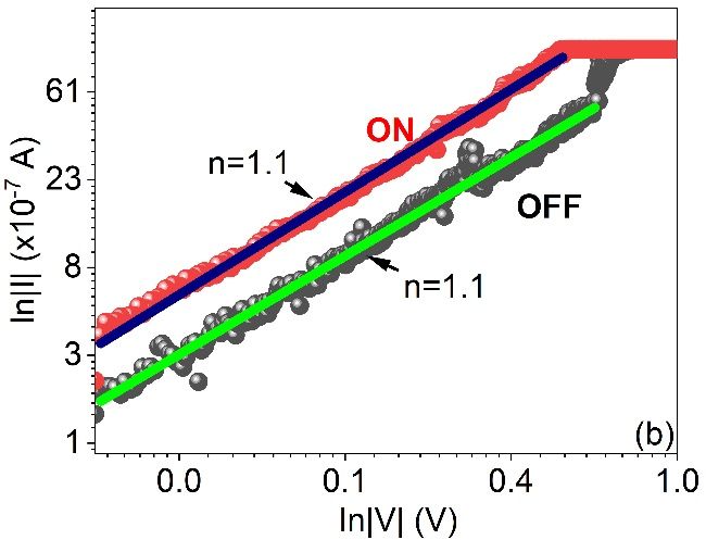
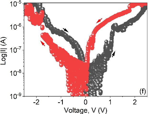
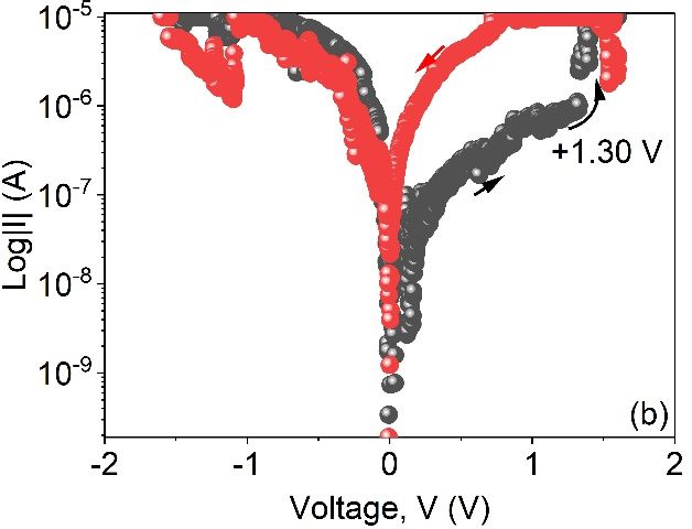
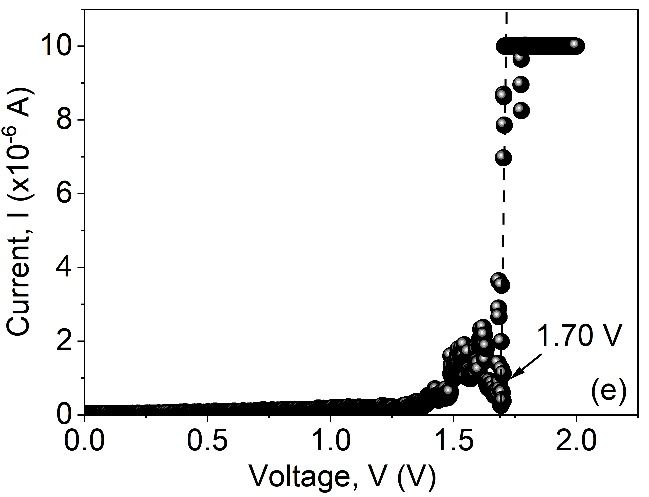
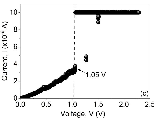
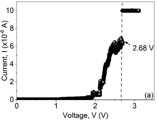
Figure 1(a). This graph reveals no current in the 0 − 1.0 regime. When the voltage ex-
ceeds 1.0 , a gradual increase in current with voltage was observed, which became more
visible beyond 1.78 V. When the voltage exceeds 2 V, a steep rise in current takes place,
leading to an abrupt jump at 2.68 V, indicating that the device is electroforming. For com-
parison, we shall look at the electroforming behaviour of devices B and C, shown in
 Figure 1(c and e), respectively. For device B, the graph reveals linear current variation with
a relatively high slope ( = 3.22 × 10⁻⁶ Ω−1 ) in the region 0 − 1.05 , followed by an
abrupt jump at 1.05 , indicating electroforming. Device C's graph, on the other hand, de-
picts a weak current variation with applied voltage ( = 1.46 × 10⁻⁷ Ω−1 ) in the 0.5 −
1.30 region, after which an increase ( = 3.41 × 10⁻⁶ Ω−1 ) in slope is observed, fol-
lowed by electroforming at 1.70 . Our results show that these three systems have different
electroforming behaviour due to varying amounts of MoS2 content on each system. Next, we
look at the semilogarithmic I-V characteristics of these devices to understand their memory
behaviour.
 Figure 1(b) shows the I-V features of device A. For this device, an increase in applied voltage
in the positive bias increased the current until a jump from a low current, i.e., high resistive state
(HRS) to high current, i.e., low resistive state (LRS), occurs at 1.30 . The HRS-to-LRS switch is called
the SET process. Upon decreasing the voltage, the device remains in the LRS, as the current did not
retrace its previous path. Thus creating an I-V hysteresis, which indicates memory behaviour. For this
device, a fair (> 102 ) ON/OFF ratio is achieved. In the negative voltage bias, the down and upsweeps
currents almost coincide and show very weak hysteresis. This indicates that the switching in this de-
vice is only in the positive voltage bias. Such memory behaviour has been reported before in
 / − 2 3 core-shell based nano-rods[17]. For device B, the semilogarithmic I-V characteristic
graph is shown in
 Figure 1(d). For this device, a low voltage switching, with = +0.60 , is observed in the pos-
itive voltage bias, and the process is not shown in the graph. However, a small hysteresis in
the negative voltage bias is also present.
 Figure 1(f) shows the semilogarithmic I-V characteristics of device C. For this device, even though
there are some minor jumps in current, the semilogarithmic I-V hysteresis resembles the 'O-type'
memory hysteresis. 'O-type' resistive switching is characterized by homogeneous gradually increas-
ing or decreasing current such that the complete cycle curve corresponds to a letter 'O'[18]. These
devices show different electroforming and memory behaviour attributed to different MoS2 weight
percentages in the active layer. In the following subsection, we shall analyze the conduction mecha-
nism on each device.
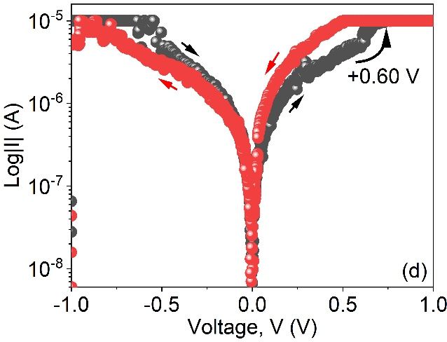
Figure 1. Current-voltage characteristics graphs depicting the (a) electroforming curve and
(b) memory behaviour of device A; (c) electroforming curve and (d) memory behaviour of
device B; and (e) electroforming and memory behaviour of device C.

3.1 Conduction mechanism
 When voltage stress, V is applied at one of the electrodes while the other electrode is
grounded, a current density, J may pass in the dielectric such that, ∝ [19]. The value of
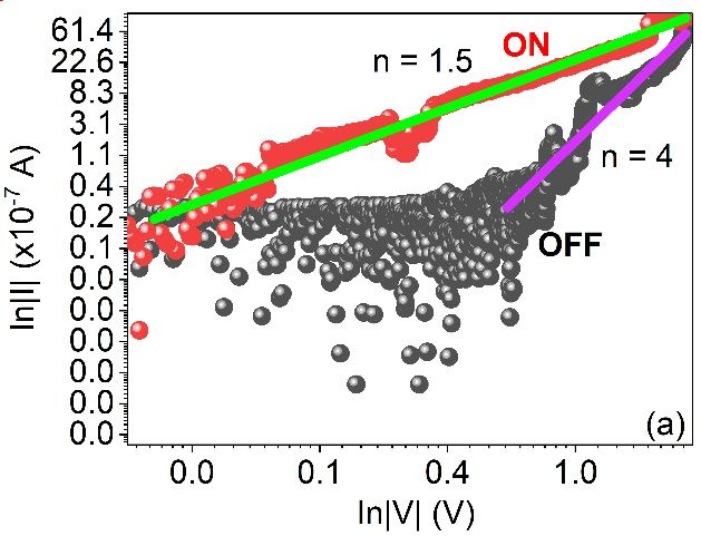
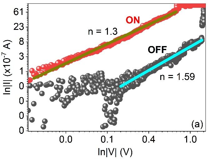
 associates with the dominant conduction mechanism and can be determined by plotting
I-V data on a log-log scale. The review article by Chiu[20] provides a summary of the already
proposed mechanisms. Figure 2(a) shows the log-log graph of device A. For this device, the
curve fitting of the ON-state current shows = 1.33~1, which implies Ohmic behaviour. The
Ohmic behaviour indicates that thermally activated charge carriers (free electrons) are re-
sponsible for the conduction, and the current is directly proportional to the applied electric
field[21–23]. The current density obeying Ohm's Law is given as[22]:

 −( − )
 ℎ = exp � � (1)

 Here is the mobility of the charge carriers, is the density of state of the conduction
band, is the energy of the conduction band, is the Fermi energy, T is the temperature
in Kelvin and is the Boltzmann constant. Ohms law indicates typical metallic conduction
due to the formation of nanoscale conduction filaments (CFs) through the active layer. CF
switching has been reported in many ReRAM systems. However, different mechanisms can
lead to the formation of CFs; therefore, we must analyze the OFF-state current behaviour.
The OFF-state current fit shows = 1.59. This obtained value of rules out both Ohmic con-
duction and the space-charge limited conduction (SCLC) mechanism, where = 2 [24]. This
is still an uncharacterized conduction mechanism. However, according to Perera et al. [24],
this current variation characteristic indicates that the ejection of carriers limits the current
at the interface.
 The log-log I-V data fitting device B is shown in Figure 2(b). Our data shows that = 1 in both the
ON- and OFF- state. The occurrence of Ohmic conduction in both LRS and HRS is is associated with a
typical electrochemical metalization (ECM) conduction mechanism, where CFs are formed through
the reduction ( + + − → ) of metal ions[24, 25]. Our systems consist of an electrochemically
active Ag electrode, but because the ECM behaviour is observed only in device B, this may suggest
that the CFs are formed through the reduction process of metal ions other than + ions. In com-
parison, more MoS2 particles are in device B than in device A. Therefore, we believe that the reduc-
tion of 4+ ions domination is more possible in device B than in device A. Which explains the dif-
ference in values for these two devices.
 Figure 3(c) shows the log-log fitting of device C. For this device = 1.5 for the ON-state, while 4
for the OFF-state. Again, = 4 implies a strong power relationship, current-voltage relationship. We
fitted this OFF-state data with different functions and found that the exponential function fits the
data perfectly, as shown in Fig. 3(b). The fitted exponential function corresponds perfectly with the
hopping conduction mechanism expression given as[26]:

 −
 = 0 + exp � � (2)

 Here, 0 is the residual current, A is a constant, is a characteristic voltage, is the Boltz-
mann constant, and is the temperature in Kelvin[26]. These results may imply that a large
amount of MoS2 content in the PVP medium provides room for electrons to hop from the
electrode to the MoS2, MoS2 to MoS2 and lastly MoS2 to the other electrode.
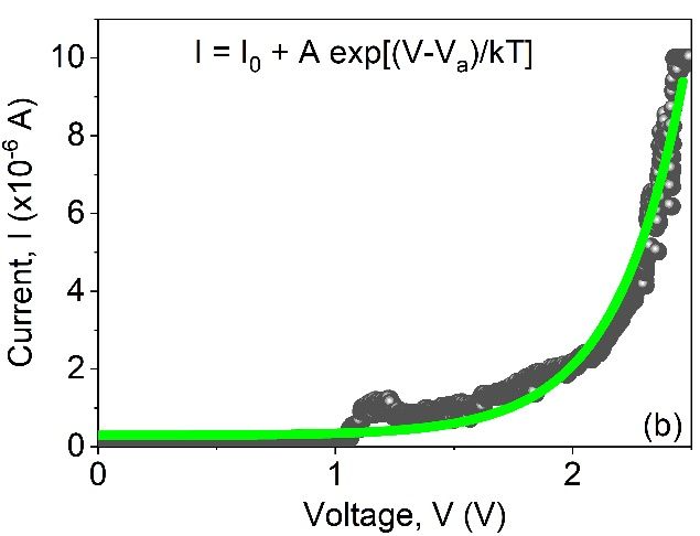
Figure 2. ln − ln curve fitting of (a) Device A and (b) Device B.

 Figure 3. (a) ln − ln curve fitting and (b) the corresponging exponential curve fitting of
the OFF-state current of Device C.

4 Conclusion
 In summary, we have fabricated the Al/PVP+MoS2/Ag ReRAM using the cost-free drop cast
method. Memory behaviour at operating voltage as low as 0.60 was achieved in the device
with 40 % MoS2 to PVP. Low operating voltage allows the device to be utilized as a low
power device. As a highlight to our results, we found that devices with different MoS2 con-
tent demonstrated different resistive switching modes and conducting mechanisms, which
implies that both memory behaviour and switching in the PVP/MoS2 composite based Re-
RAMs can be exploited by controlling the amount of MoS2.

Acknowledgements
Zolile acknowledges the financial support from the DHET-nGAP program provided through Central
University of Technology.
References

1. N. Raeis-hosseini and J. Lee, 223 (2017).doi:10.1007/s10832-017-0104-z
2. S. Liu, S. Dong, X. Wang, L. Shi, H. Xu, S. Huang, and J. Luo, Nanotechnology 31 (2020).
3. J. Xu, X. Zhao, Z. Wang, H. Xu, J. Hu, J. Ma, and Y. Liu, Small 15, 1803970 (2019).
4. N. R. Hosseini and J. S. Lee, Adv. Funct. Mater. 25, 5586 (2015).
5. S. Vallabhapurapu, L. D. Varma Sangani, M. Ghanashyam Krishna, V. V. Srinivasu, C.
 Du, S. Du, and A. Srinivasan, Mater. Today Proc. 9, 615 (2019).
6. S. Yu, Synth. Lect. Emerg. Eng. Technol. 2, 1 (2016).
7. T. W. Hickmott, J. Appl. Phys. 33, 2669 (1962).
8. D. S. Jeong, R. Thomas, R. S. Katiyar, J. F. Scott, H. Kohlstedt, A. Petraru, and C. S.
 Hwang, Reports Prog. Phys. 75, 076502 (2012).
9. B. Nair, Int. J. Toxicol. 17, 95 (1998).
10. A. Rawat, H. K. Mahavar, A. Tanwar, and P. J. Singh, Bull. Mater. Sci. 37, 273 (2014).
11. M. Ravi, S. Bhavani, K. Kiran Kumar, and V. V. R. Narasimaha Rao, Solid State Sci. 19,
 85 (2013).
12. M. Liu, X. Yan, H. Liu, and W. Yu, React. Funct. Polym. 44, 55 (2000).
13. C. V. S. Reddy, A. Jin, X. Han, Q. Zhu, L. Mai, and W. Chen, 8, 279 (2006).
14. N. Bai, M. Xu, C. Hu, Y. Ma, Q. Wang, D. He, J. Qi, and Y. Li, Mater. Sci. Semicond.
 Process. 91, 246 (2019).
15. Z. Wu, T. Wang, C. Sun, P. Liu, B. Xia, J. Zhang, Y. Liu, and D. Gao, 125213 (2017).
16. M. M. Rehman, G. U. Siddiqui, J. Z. Gul, S. W. Kim, J. H. Lim, and K. H. Choi, Sci. Rep. 6,
 1 (2016).
17. D. Sarkar and A. K. Singh, J. Phys. Chem. C 121, 12953 (2017).
18. D. Prime and S. Paul, Philos. Trans. R. Soc. A Math. Phys. Eng. Sci. 367, 4141 (2009).
19. Y. Liu, P. Gao, X. Jiang, L. Li, J. Zhang, and W. Peng, J. Appl. Phys. 116 (2014).
20. F. Chiu, Adv. Mater. Sci. Eng. 2014, 1 (2014).
21. E. Lim and R. Ismail, Electronics 4, 586 (2015).
22. S. Qin, R. Dong, X. Yan, and Q. Du, Org. Electron. 22, 147 (2015).
23. R. Perera, A. Ikeda, R. Hattori, and Y. Kuroki, Microelectron. Eng. 65, 357 (2003).
24. Z. Shen, C. Zhao, Y. Qi, W. Xu, Y. Liu, I. Z. Mitrovic, L. Yang, and C. Zhao, Nanomaterials
 10, 1 (2020).
25. N. Raeis-Hosseini, S. Lim, H. Hwang, and J. Rho, Adv. Electron. Mater. 4 (2018).
26. S. Vallabhapurapu, A. Rohom, N. B. Chaure, C. Tu, S. Du, V. V. Srinivasu, and A.
 Srinivasan, Appl. Phys. A 124, 639 (2018).
You can also read