CONFERENCE 79th PHYSICAL ELECTRONICS - University of Central Florida - PEC 2019
←
→
Page content transcription
If your browser does not render page correctly, please read the page content below
79th PHYSICAL ELECTRONICS
 CONFERENCE
PROGRAM AND ABSTRACT BOOK

 University of Central Florida
 Harris Corporation Engineering Center
 June 2-5, 2019
2
79th ANNUAL PHYSICAL
 ELECTRONICS CONFERENCE
 WORKING PROGRAM
 June 2-5, 2019
 Harris Corporation Engineering Center
 University of Central Florida, Orlando, FL

SPONSORS
AMERICAN VACUUM SOCIETY
SCIENTA OMICRON
SPECS
SIGMA SURFACE SCIENCE
LEYBOLD
THERMO FISHER SCIENTIFIC
CREATEC SENTYS
ANCORP
UCF OFFICE OF RESEARCH
UCF COLLEGE OF SCIENCES
UCF COLLEGE OF ENGINEERING AND COMPUTER SCIENCE
UCF NANOSCIENCE AND TECHNOLOGY CENTER
UCF DEPARTMENT OF PHYSICS
UCF FACULTY CLUSTER INITIATIVE

 3
PEC GENERAL ORGANIZING COMMITTEE
Brian Swartzentruber (Chair) Sandia Laboratories
Karsten Pohl (Treasurer) University of New Hampshire
Carl Ventrice (co-Treasurer) CNSE, University of Albany, SUNY
Daniel Dougherty North Carolina State University
Jane Hinch Rutgers University
Seth King University of Wisconsin-La Crosse
Paul Thibado University of Arkansas, Fayetteville
Nicholas Strandwitz Lehigh University

 PEC LOCAL ORGANIZING COMMITTEE
Talat Rahman (Chair) University of Central Florida
William Kaden University of Central Florida
Mihai Vaida University of Central Florida
Parag Banerjee University of Central Florida
Laurene Tetard University of Central Florida
Zahra Hooshmand University of Central Florida
Duy Le University of Central Florida

 4
SPONSORS
We enthusiastically thank the following sponsors for supporting PEC 2019.

 NOTTINGHAM PRIZE SPONSOR

 POSTER PRIZE SPONSOR

 GENERAL SPONSORS

OFFICE OF RESEARCH
COLLEGE OF SCIENCES
DEPARTMENT OF PHYSICS
FACULTY CLUSTER INITIATIVE
NANOSCIENCE & TECHNOLOGY CENTER
COLLEGE OF ENGINEERING & COMPUTER SCIENCE

 5
HISTORY OF PEC
The 79th Physical Electronics Conference at the University of Central Florida follows
in the tradition of annual PEC meetings held on university campuses and research
labs in North America. This topical conference provides a yearly forum for the
dissemination and discussion of novel and fundamental theoretical and experimental
research in the physics, chemistry, biology, and engineering of surfaces and
interfaces. It includes the prestigious Nottingham Prize competition for best
presentation based on doctoral research. Over 75 years the emphases of the
conference have changed, yet the meeting remains centered in its basis of
fundamental science at material interfaces. Central themes now include the
interfaces of metals, semiconductors, ionic conductors, dielectrics, insulators, fluids,
porous materials, and the wealth of biomaterials.

Physicists, chemists, and engineers, with interests in these fields, come together to
present and discuss experimental and theoretical research on exposed (gas-solid or
gas-liquid) surfaces, or buried (liquid-solid and solid-solid) interfaces.
Representative topics include (but are not limited to) electronic, chemical, magnetic,
and structural properties of interfaces; energetics, kinetics, and dynamics of physical
and chemical transformations at surfaces; formation, assembly, structural and
electronic properties, and modeling of nanoscale surface architectures; effects of
electron correlation at surfaces, and topological insulators; interfacial interactions of
biological materials; impacts of interface chirality; mechanisms of film growth and
interface evolution; and transfer of energy, electrons, or ions across materials
interfaces. New methods/techniques for interrogation of interfaces, novel devices or
sensors, and new applications for structurally and chemically tailored interfaces also
fall within the scope of this meeting.

 6
PREVIOUS PEC HOSTS
1966 Massachusetts Institute of Technology 1993 Rensselaer Polytechnic Institute
1967 Massachusetts Institute of Technology 1994 University of Tennessee
1968 University of Minnesota 1995 Arizona State University
1969 Yale University 1996 Boston University
1970 University of Wisconsin - Milwaukee 1997 University of Oregon
1971 National Bureau of Standards 1998 Pennsylvania State University
1972 Sandia Laboratories 1999 University of California - Berkeley
1973 University of California - Berkeley 2000 Louisiana State University
1974 Bell Laboratories 2001 Sandia National Laboratories
1975 Pennsylvania State University 2002 Georgia Institute of Technology
1976 University of Wisconsin-Madison 2003 Cornell University
1977 Stanford University 2004 University of California – Davis
1978 Oak Ridge National Laboratory 2005 University of Wisconsin - Madison
1979 University of Maryland 2006 Princeton University
1980 Cornell University 2007 University of Illinois, Urbana-Champaign
1981 Montana State University 2008 University of California - Riverside
1982 Georgia Institute of Technology 2009 Rutgers University
1983 Sandia National Laboratories 2010 University of Wisconsin - Milwaukee
1984 Princeton University 2011 University at Albany
1985 University of Wisconsin - Milwaukee 2012 University of Texas - Dallas
1986 University of Texas - Austin 2013 North Carolina State University
1987 IBM Almaden Research 2014 University of Wisconsin - La Crosse
1988 Brookhaven National Laboratory 2015 Rutgers University - New Brunswick
1989 University of Washington 2016 University of Arkansas - Fayetteville
1990 National Institute of Standards 2017 Portland State University
1991 Rutgers University – Piscataway 2018 University of New Hampshire
1992 University of California - Irvine

 7
NOTTINGHAM PRIZE
The Nottingham Prize was originally established in 1966 from contributions given in memory of
Professor Wayne B. Nottingham of the Massachusetts Institute of Technology by his many friends
and associates. The prize, currently consisting of a certificate and $1,500, is awarded to the best
student paper presented at the conference. This prize represents a seminal honor since many
Nottingham winners have gone on to become leaders in the field of surface science. In addition,
you and your advisor’s names are added to the Nottingham Wikipedia website.

 PREVIOUS NOTTINGHAM WINNERS
Year Winner Institution PI
1966 L. F. Cordes University of Minnesota W. T. Peria
1967 D. Steiner Massachusetts Institute of Technology E. P. Gyftopoulos
 J.V. Hollweg Massachusetts Institute of Technology E. P. Gyftopoulos
1968 E. Ward Plummer Cornell University T. N. Rhodin
1969 John C. Tracy Cornell University J. M. Blakely
1970 J. M. Baker Cornell University J. M. Blakely
1971 D. P. Smith University of Minnesota W. T. Peria
1972 W. Henry Weinberg University of California, Berkeley R. Merrill
1973 J. R. Bower Bartol Research Foundation J. M. Chen
1974 N. J. Dionne Cornell University T. N. Rhodin
 T. Gustafsson Chalmers University of Technology P. O. Nillson
1975 L. C. Isett Cornell University J. M. Blakely
1976 J. A. Knapp Montana State University G. A. Lapeyre
1977 S.-L. Weng University of Pennsylvania E. W. Plummer
1978 Gwo-Ching Wang University of Wisconsin, Madison M. G. Lagally
1979 Wilson Ho University of Pennsylvania E. W. Plummer
1980 R. Di Foggio University of Chicago R. Gomer
 Harry J. Levinson University of Pennsylvania E. W. Plummer
1981 Ruud M. Tromp FOM Institute for Atomic & Molecular F. W. Saris
 Physics
1982 P. O. Hahn University of Hanover M. Henzler
1983 R. Raue University of Köln (Cologne) and KFA G. Güntherodt & M.
 Jülich Campagna
1984 M. Onellion Rice University G. K. Walters
1985 K. Gibson University of Chicago S. J. Sibener
 J. W. M. Frenken FOM Institute for Atomic & Molecular J. F. van der Veen
 Physics
1986 S. M. Yalisove University of Pennsylvania W. R. Graham
1987 John D. Beckerle Massachusetts Institute of Technology S. T. Ceyer
1988 Lee J. Richter Cornell University W. Ho
1989 J.-K. Zuo Rensselaer Polytechnic Institute C.-C. Wang
1990 Y.-W. Mo University of Wisconsin, Madison M. G. Lagally
1991 B. Swartzentruber University of Wisconsin, Madison M. B. Webb

 8
1992 Thomas Michely KFA Jülich G. Comsa
1993 A. K. Swan Boston University M. El-Batanouny
1994 G. Rosenfeld KFA Jülich G. Comsa
1995 Marcus K. Weldon Harvard University C. Friend
1996 J. Carpinelli University of Tennessee E. W. Plummer
 B. Kohler Fritz Haber Institute M. Scheffler
1997 D. Gragson University of Oregon G. Richmond
1998 Barry C. Stipe Cornell University W. Ho
 M. S. Hoogeman FOM Institute & Leiden Univ. J. W. M. Frenken
1999 K. Pelhos Rutgers University T. E. Madey
2000 Lincoln Lauhon Cornell University W. Ho
2001 Gayle Thayer University of California, Davis & Sandia S. Chiang & R.
 Livermore Hwang
2002 Denis Potapenko Rutgers University B. J. Hinch
2003 John Pierce University of Tennessee E. W. Plummer & J.
 Shen
2004 Peter Wahl Max Planck Inst. for Solid-State Physics K. Kern
2005 Nathan Guisinger Northwestern University M. Hersam
2006 Mustafa M. Ozer University of Tennessee-Knoxville J. R. Thompson & H.
 H. Weitering
 Paul C. Snijders Delft University of Technology H. H. Weitering & T.
 M. Klapwijk
2007 P. Maksymovych University of Pittsburgh J. T. Yates, Jr.
2008 Brett Goldsmith University of California, Irvine P. G. Collins
2009 Alpha T. N' Diaye University of Köln (Cologne) T. Michely
2010 Heather Tierney Tufts University C. Sykes
2011 Tanza Lewis University of California, Irvine J. Hemminger & B.
 Winter
2012 Daniel Schwarz University of Twente B. Poelsema
2013 Benjamin A. Gray University of Arkansas - Fayetteville J. Chakhalian
2014 Donna A. Kunkel University of Nebraska - Lincoln A. Enders
2015 Christoph Große Max Planck Inst. for Solid State Physics K. Kern
 Amanda Larson University of New Hampshire K. Pohl
2016 Charlotte Herbig University of Köln (Cologne) T. Michely
2017 Erik S. Skibinski Cornell University M. A. Hines
2018 Felix Lüpke FZ Julich B. Voigtländer

 9
PROGRAM SUMMARY
 SUNDAY
4:00 – 6:00 PM Check In Libra Community Area Office
5:00 – 8:00 PM Welcome Reception Physical Sciences Building Atrium
 MONDAY
7:45 – 8:45 AM Breakfast, Registration, and HCEC Atrium
 Setup of Posters and Exhibits
8:45 – 9:00 AM Opening Remarks HCEC 101
9:00 – 10:00 AM Oral Presentations HCEC 101
10:00 – 10:20 AM Coffee Break HCEC Atrium
10:20 – 11:00 AM Keynote Presentation HCEC 101
 Donna Chen, University of South Carolina
11:00 – 12:20 PM Oral Presentations HCEC 101
12:20 – 1:20 PM Lunch HCEC Atrium
1:20 – 2:00 PM Keynote Presentation HCEC 101
 Vincent Smentkowski, General Electric
2:00 – 3:00 PM Oral Presentations HCEC 101
3:00 – 3:20 PM Coffee Break HCEC Atrium
3:20 – 4:00 PM Oral Presentations HCEC 101
4:00 – 6:00 PM Poster Session HCEC Atrium
6:30 – 8:30 PM Annual Picnic Rahman Residence
8:30 – 9:30 PM General Committee Meeting Rahman Residence
 TUESDAY
8:00 – 9:00 AM Breakfast HCEC Atrium
9:00 – 9:20 AM Oral Presentation HCEC 101
9:20 – 10:00 AM Keynote Presentation HCEC 101
 Bjørk Hammer, Aarhus University
10:00 – 10:20 AM Coffee Break HCEC Atrium
10:20 – 12:00 PM Nottingham Presentations HCEC 101
12:00 – 1:00 PM Lunch HCEC Atrium
1:00 – 2:00 PM Lab Tours Details provided at meeting
2:00 – 3:15 PM Nottingham Presentations HCEC 101
3:15 – 3:35 PM Coffee Break HCEC Atrium

 10
3:35 – 4:50 PM Nottingham Presentations HCEC 101
4:50 – 5:30 PM Student Involvement & Networking HCEC 101
6:30 – 8:30 PM Nottingham Banquet Details provided at meeting
8:30 – 10:30 PM Nottingham Celebration Details provided at meeting

 WEDNESDAY
7:00 – 9:00 AM Check Out Libra Community Area Office
8:00 – 8:50 AM Breakfast HCEC Atrium
8:50 – 9:30 AM Invited Presentation HCEC 101
 Ludwig Bartels, UC – Riverside
9:30 – 10:10 AM Oral Presentations HCEC 101
10:10 – 10:30 AM Coffee Break HCEC Atrium
10:30 – 11:30 AM Oral Presentations HCEC 101
11:30 – 11:45 AM Closing remarks HCEC 101
11:45 AM Lunch HCEC Atrium

 11
CONFERENCE AGENDA
 SUNDAY
4:00 – 6:00 PM Check In Libra Community Area Office
5:00 – 8:00 PM Welcome Reception Physical Sciences Building Atrium

 12
MONDAY
7:45 – 8:45 AM Breakfast, Registration, and Harris Corporation
 Setup of Posters and Exhibits Engineering Center

8:45 – 9:00 AM Opening Remarks

9:00 – 10:00 AM Session 1: William Kaden, University of Central Florida
 9:00 AM O.1 Sulfur-Metal Interactions on Ag(100) and Ag(110) at Low Coverages
 Peter Spurgeon
 9:20 AM O.2 Defect-laden Hexagonal Boron Nitride for the Reduction of Carbon
 Dioxide
 Richard Blair
 9:40 AM O.3 Electrochemical Catalysis at Grain-Boundary Surface Sites
 Xiaofeng Feng

10:00 – 10:20 AM Coffee Break

10:20 – 11:00 AM Keynote Presentation
 K.1 Designing New Heterogeneous Catalysts Through Metal-Metal
 Interactions
 Donna Chen, Department of Chemistry & Biochemistry, University of
 South Carolina

11:00 – 12:20 PM Session 2: Seth King, University of Wisconsin – La Crosse
 11:00 AM O.4 Defect engineering of 2D-Transition Metal Dichalcogenides by
 Incorporation of Excess Metal Atoms into its Crystal Structure
 Paula Coelho
 11:20 AM O.5 Atomically Precise Graphene Nanoribbons: From Synthesis to Devices
 Alexander Sinitskii
 11:40 AM O.6 Fluctuation-Induced Transport from Freestanding Graphene
 Paul Thibado
 12:00 PM O.7 Nitrogen vacancy on hexagonal boron nitride as single orbital catalyst: A
 first principles study
 Duy Le

12:20 – 1:20 PM Lunch

 13
1:20 – 2:00 PM Keynote Presentation K.2 The Importance of Surface Modification and Analysis in the Industrial Sector Vincent Smentkowski, Structural Materials Characterization, General Electric Global Research Center 2:00 – 4:00 PM Session 3: Paul Thibado, Univ. of Arkansas, Fayetteville 2:00 PM O.8 Mechanistic understanding of hydrocarbon fuels formation via CO hydrogenation reaction on 2D catalytic materials Mihai Vaida 2:20 PM O.9 Crystal Structure Reconstruction on Surface of Quantum Spin Liquid Candidate -RuCl3 Zhongwei Dai 2:40 PM O.10 Nonvolatile voltage controlled molecular spin state switching Peter Dowben 3:00 – 3:20 PM Coffee Break 3:20 PM O.11 Defect Doping ZnO Thin-Films with - Radiation Seth King 3:40 PM O.12 Rational Computational Design of Efficient Electro-catalysts for Hydrogen Fuel Cell Cathodes Sergey Stolbov 4:00 – 6:00 PM Poster Session Atrium 6:30 – 8:30 PM Annual Picnic Rahman Residence 8:30 – 9:30 PM General Committee Meeting Rahman Residence 14
TUESDAY
8:00 – 9:00 AM Breakfast Harris Corporation
 Engineering Center
9:00 – 9:20 AM Oral Presentation
 O.13 Reduced Graphene Oxide-Mediated Gold/Cobalt Oxide Catalyst with
 Strong Metal-Support Interaction for CO Oxidation
 Shouhua Xie

9:20 – 10:00 AM Keynote Presentation
 K.3 Machine learning for atomistic structure search
 Bjørk Hammer, Department of Physics and Astronomy, Aarhus University

10:00 – 10:20 AM Coffee Break

10:20 – 12:00 PM Nottingham Session 1:
 Brian Swartzentruber, CINT/Sandia Nat’l Labs
 10:20 AM N.1 Mechanistic Studies of Reducible Metal Oxides as Hydrodeoxygenation
 Catalysts
 Akbar Mahdavi-Shakib
 10:45 AM N.2 Redox active Organic Chains on Au(111) for single site catalysis: A first-
 principles study
 Naseem Ud Din
 11:10 AM N.3 Encapsulation of Metal Nanoparticles Near the Surface of Graphite
 Ann Lii-Rosales
 11:35 AM N.4 Well-Defined Pt/CeO2 catalysts synthesized by Atomic Layer Deposition
 Bochuan Song

12:00 – 1:00 PM Lunch

1:00 – 2:00 PM Laboratory Tours

2:00 – 3:15 PM Nottingham Session 2:
 Carl Ventrice, SUNY Polytechnic Institute
 2:00 PM N.5 Normal-Stress-Induced Mechanochemical Decomposition of Methyl
 Thiolates on Cu(100)
 Alejandro Boscoboinik
 2:25 PM N.6 Symmetry Considerations for Interactions on MoS2
 Prescott Evans
 2:50 PM N.7 Distinct multiple fermionic states in a single topological metal
 M. Mofazzel Hosen

 15
3:15 – 3:35 PM Coffee Break

3:35 – 4:50 PM Nottingham Session 3:
 Karsten Pohl, University of New Hampshire
 3:35 PM N.8 Oxidation of Semiconductors and Semimetals by Supersonic Beams of O2
 with Scanning Tunneling Microscopy Visualization
 Ross Edel
 4:00 PM N.9 Growth and Characterization of Large-Area Ultrathin InSe
 Hadallia Bergeron
 4:25 PM N.10 Borophene and its Functionalization
 Xiaolong Liu

4:50 – 5:30 PM Student Involvement & Networking Opportunity

6:30 – 8:30 PM Nottingham Banquet Details Provided at Meeting
8:30 – 10:30 PM Nottingham Celebration Details Provided at Meeting

 16
WEDNESDAY 7:00 – 9:00 AM Check Out Libra Community Area Office 8:00 – 8:50 AM Breakfast Harris Corporation Engineering Center 8:50 – 9:30 AM Invited Presentation I.1 Preparation of Transition Metal Di- and Trichalcogenides: From vdW Semiconducting Films to vdW 1D Metallic Nanowires Ludwig Bartels, Department of Chemistry, University of California – Riverside 9:30 – 10:10 AM Session 4: Talat Rahman, University of Central Florida 9:30 AM O.14 3d Molecular assembly structure and tilt-angle evaluation with non- contact AFM Karsten Pohl 9:50 AM O.15 Development and characterization of MoN/Ru(0001) and Mo2N/Ag(100) thin-films for model-catalysis applications William Kaden 10:10 – 10:30 AM Coffee Break 10:30 – 11:30 AM Session 5: Mihai Vaida, University of Central Florida 10:30 AM O.16 Rubrene vs. fluorine-functionalized reubrene molecules on a metal surface: self-assembly, electronic structure and energy alignment of a monolayer of Ag(100) Jonathan Viereck 10:50 AM O.17 Electron Induced Disordering and Decomposition of SAMs Carl Ventrice 11:10 AM O.18 The molecule deprotonation and the excitation spectrum of Ag44(MNBA)2, Zahra Hooshmand 11:30 – 11:45 AM Closing Remarks 11:45 AM Boxed Lunch 17
ABSTRACT BOOK
 KEYNOTE PRESENTATIONS
Pages K.1 – K.3
 INVITED PRESENTATION
Page I.1
 NOTTINGHAM PRESENTATIONS
Pages N.1 – N.10
 ORAL PRESENTATIONS
Pages O.1 – O.18
 POSTER PRESENTATIONS
Pages P.1 – P.18

 18
KEYNOTE

 Designing New Heterogeneous Catalysts Through Metal-Metal
 Interactions
 Donna A. Chen, Amy J. Brandt, Thathsara D. Maddumapatabandi, Deependra M. Shakya, and
 Sharfa Farzandh

Department of Chemistry and Biochemistry, University of South Carolina, 631 Sumter Street, Columbia,
 SC, 29208, USA

 Email: dachen@sc.edu

Bimetallic catalysts often exhibit superior activity compared to their monometallic counterparts. The
bimetallic Pt-Re system has been used for decades in industrial reforming reactions, and more recently Pt-
Re catalysts have demonstrated enhanced activity for the water gas shift (WGS) reaction and aqueous phase
reforming of polyols. However, the exact origins of the superior activity of Pt-Re over pure Pt are not fully
understood; specifically little is known about the role of oxidized Re under reaction conditions. In order to
understand this improved activity of Pt upon addition of Re, it is necessary to control bimetallic cluster
composition, cluster sizes and oxidation states of the Re, as well as to probe Re oxidation states under
reaction conditions. We have prepared and characterized Pt-Re bimetallic clusters on titania, which is the
most active support for WGS. Experiments were carried out in an ultrahigh vacuum chamber directly
coupled to a microreactor so that activity could be evaluated under catalytically relevant pressures while
surfaces could be characterized using X-ray photoelectron spectroscopy and infrared absorption reflection
spectroscopy before and after reaction. The greatest WGS activity was observed for surfaces consisting of
Pt on Re. While the presence of rhenium oxide did not improve catalytic activity, Pt-Re interactions were
found to decrease CO poisoning on the bimetallic catalyst. The role of metal-support interactions was
investigated by depositing bimetallic clusters on a non-interacting graphite support and comparing with
activity on titania.

 K.1
KEYNOTE
The Importance of Surface Modification and Analysis in the Industrial Sector
 Vincent Smentkowski
 General Electric – Research, Structured Materials - Characterization, 1 Research Circle, Building K1
 1d41, Niskayuna, NY, 12309, USA
 Email: smentkow@ge.com
 The composition, microstructure, phase, chemical bonding, electronic states, and/or texture at the
surfaces of material is often different than that of the bulk. The outer surface is where many material
interactions/reactions take place [1,2,3]. Surface scientists and analysts are grouped into three different
categories: (1) researchers that perform a complete characterization of clean, single crystal surfaces, (2)
researchers that study the interaction of adsorbates onto clean surfaces under ultrahigh vacuum conditions,
or (3) researchers that are analyzing as-received, real-life parts. The first two groups of scientists are often
trying to understand fundamental phenomena under well controlled conditions and are often in academia.
The later group of researchers, are often found in an industrial setting, and are usually classified as applied
surface scientists/analysts. Often their samples contain multiple components and as the samples are
transferred from ambient conditions into the surface analysis instrument, are not clean.
 The field of surface analysis rapidly grew in the late 1960’s and early 1970’s with the introduction
of commercial surface analysis instrumentation [1,2, 3]. It is of interest and importance to note that the first
surface analysis instruments such as Auger Electron Spectroscopy (AES) [4-6], X-ray Photoelectron
Spectroscopy (XPS) [7], Ion Scattering Spectroscopy (ISS) [8] and Secondary Ion Mass Spectroscopy
(SIMS) [9, 10] were developed at, or in collaboration with, industrial research laboratories such as General
Electric[4-6], Hewlett-Packard [7], 3M [8], Knolls Atomic Power Laboratory-General Electric [9, 10],
respectively. These first surface analysis instruments were designed and built to study practical phenomena
in real material systems.
 My talk will summarize my career path, which started with studies of adsorbates on atomically
clean single crystal substrates and developed into performing surface analysis on real life samples to support
the development of next generation industrial materials and products. The roles both professional societies
and collaborations (both internal within GE and external) had will be highlighted. I will discuss the
characterization challenges faced in an industrial setting where the surface analyst is often provided non-
ideal samples and is asked to provide both a rapid and complete analysis of the sample. The criticality of
talking with the person that submits the sample to understand their issue(s) and what they expect from the
analysis (as well as being certain they realize possible complications) will be highlighted via real samples.
References:
[1], C.B. Duke, J. Vac. Sci. Technol A 2(2) (1984) 139
[2] Introduction to Surface Chemistry and Catalysis, 2nd Ed., Gabor A Somorjai and Yimin Li Eds, John
Wiley and Sons, 2010.
[3] Surface Analysis and Techniques in Biology, Vincent S. Smentkowski, Editor, Springer, 2014.
[4] L.A. Harris, General Electric Rept No 67-C-201 (1967); J. Appl Phys. 39 (1968) 1419
[5] L.A. Harris J. Vac. Sci. Technol 11 (1974) 23
[6] G. Gergely, Vacuum 45 (2/3) (1994) 311
[7] In cooperation with Siegbahn, a group of engineers from Hewlett-Packard in the USA (Mike Kelly,
Charles Bryson, Lavier Faye, Robert Chaney) produced the first commercial monochromatic XPS
instrument in 1969; http://en.wikipedia.org/wiki/X-ray_photoelectron_spectroscopy ; M. A. Kelly, J.
Chem. Educ, 81(12) (2004) 1726.
[8] D.P. Smith, J. Appl Phys 38 (1967) 340; P. S. Wang, W. E. Moddeman, L. D. Haws, T. N. Wittberg, J.
A. Peters “Surface Studies of Plastic-Bonded E£TN and RDX by X-Ray Photoelectron Spectroscopy (XPS)
and Ion-Scattering Spectroscopy (ISS)” http://www.osti.gov/bridge/servlets/purl/6254094/6254094.pdf
[9] J.A. McHugh and J.C. Sheffield, J. Applied Physics 35 (3) (1964) 512.
[10] J.A. McHugh and J.C. Sheffield Anal. Chem. 39(3) (1967) 377

 K.2
KEYNOTE

 Machine learning for atomistic structure search
 Bjørk Hammer

Department of Physics and Astronomy, Aarhus University, Ny Munkegade 120, Building 1520, DK-8000
 Aarhus C, Denmark

 Email: hammer@phys.au.dk

During structure search with Density Functional Theory (DFT) databases of structure-energy relations are
established that may be used to direct and speed up the structure search itself. In this talk, I describe how
machine learning methods such as clustering and regression may assist Monte Carlo [1] and evolutionary
search methods [2-5] in finding the optimum structure of molecules and inorganic surface reconstructions.
One key element of using machine learning methods in conjunction with DFT is the possibility of
decomposing the total DFT energy into atomic contributions. Owing to the nature of the Kohn-Sham
equations (the one-electron Schrödinger Equation) such a decomposition is ordinarily not supported.
Nonetheless, our experience shows that the atomic energies are highly meaningful and lead to a speed up
of the structure determination when used appropriately. As a final topic, I will demonstrate a search strategy
in which the computer collects knowledge of atomistic interactions while searching, which eventually
enables it to search in a rational way [6]. This approach combines image recognition and reinforcement
learning strategies and follow the recent advancements by Google Deep Mind in their development of the
Alpha Go Zero method for playing the board game Go.

[1] Machine learning enhanced global optimization by clustering local environments to enable bundled
atomic energies, S.A. Meldgaard, E.L. Kolsbjerg, B Hammer, The Journal of Chemical Physics 149,
134104 (2018).
[2] Exploration versus exploitation in global atomistic structure optimization, M.S. Jørgensen, U.F. Larsen,
K.W. Jacobsen, B. Hammer, The Journal of Physical Chemistry A 122, 1504-1509 (2018).
[3] On-the-fly machine learning of atomic potential in density functional theory structure optimization, T.L.
Jacobsen, M.S. Jørgensen, B. Hammer, Physical Review Letters 120, 026102 (2018).
[4] Atomic energies from a convolutional neural network, X Chen, M.S. Jørgensen, J Li, B Hammer,
Journal of Chemical Theory and Computation 14 (7), 3933-3942 (2018).
[5] Neural-network-enhanced evolutionary algorithm applied to supported metal nanoparticles, E.L.
Kolsbjerg, A.A. Peterson, B Hammer, Physical Review B 97 (19), 195424 (2018).
[6] Atomistic Structure Learning, M.S. Jørgensen, H.L. Mortensen, S.A. Meldgaard, E.L. Kolsbjerg, T.L.
Jacobsen, https://arxiv.org/abs/1902.10501.

 K.3
INVITED

 Preparation of Transition Metal Di- and Trichalcogenides: From
 vdW Semiconducting Films to vdW 1D Metallic Nanowires
 Ludwig Bartels

Department of Chemistry, University of California, Riverside, 124 Pierce Annex, Riverside, CA, 92521,
 USA

 Email: bartels@ucr.edu

The transition metal triselenide (TMT) TaSe3 consist of Ta-Se3-Ta-Se3- stacks in which the central Ta-
atoms column is separated from adjacent ones by a vdW gap owing to the Se3 trimers, much similar to how
the Mo-atoms plane in MoSe2 is separated from the adjacent ones by vdW gaps owing to the Se planes on
each of its sides. TaSe3 is metallic; motivated by the presence of a vdW gap between neighboring wires, we
explored the cross-section dependent conductivity of the material along the wire direction. We found it to
be unaffected by the wire dimension even down to 7nm, the smallest wires we could contact successfully.
This is much different than what is observed for bulk conductors like copper, where the wire resistance
increases dramatically as the wire dimension is decreases below the electron mean free path. Moreover, the
current density that the nanowires can endure are on the order of ~108 A/cm2 and an electromigration energy
barrier more than twice that of copper is found. In this talk, I will present how the TaSe3 nanowires are
synthesized via chemical vapor deposition (CVD) on a SiO2/Si substrates at a temperature compatible with
industry-standard back-end-of-line (BEOL) processing. The results show the potential that these quasi 1D
van der Waals TMTs have for downscaled interconnect applications. Time permitting, I will also speak
about our recent achievement in process control in the deposition of TMD films leading to wafer scale
material.

 I.1
NOTTINGHAM

 Mechanistic Studies of Reducible Metal Oxides as
 Hydrodeoxygenation Catalysts
 A. Mahdavi-Shakib1,2,3* and B. G. Frederick1,2,3
 *Nottingham Contestant
 1
 Laboratory for Surface Science and Technology (LASST),
 2
 Forest Bioproducts Research Institute (FBRI),
 3
 Dept. of Chemistry, University of Maine, Orono, ME 04469

 Email: akbar.mahdavi@maine.edu
Hydrodeoxygenation (HDO) reactions are a class of reactions that remove oxygen from molecules as H2O
using H2 gas and a catalyst. Ruthenium supported titania (Ru/TiO2) catalysts are excellent catalysts for
HDO of phenol to benzene,[1] an important reaction for the conversion of lignin part of biomass to biofuels.
In the proposed mechanism, [2] HDO reaction takes place at the interface of Ru and TiO2, surface hydroxyls
with basic character are required, and water acts as a co-catalyst.[2] We showed that HDO rates and
selectivities of Ru/TiO2 catalysts strongly vary depending on the support crystal structure and preparation
conditions. Surface hydroxyls of different TiO2 samples (anatase, rutile, and pyrogenic) were identified
using diffuse reflectance infrared Fourier transform spectroscopy (DRIFTS) experiments performed on
vigorously cleaned surfaces and a facet-specific assignment was proposed using density functional theory
(DFT) calculations performed by our collaborators. Electronic structure of TiO2 samples were studied using
the reaction of vigorously cleaned TiO2 samples with H2/D2. Our results are used to derive structure-activity
relationships for the Ru/TiO2 catalyzed HDO reactions.
References:
[1] C. Newman, X. Zhou, B. Goundie, I.T. Ghampson, R.A. Pollock, Z. Ross, M.C. Wheeler, R.W.
Meulenberg, R.N. Austin, B.G. Frederick, Effects of support identity and metal dispersion in supported
ruthenium hydrodeoxygenation catalysts, Applied Catalysis A: General, 477 (2014) 64-74.

[2] R.C. Nelson, B. Baek, P. Ruiz, B. Goundie, A. Brooks, M.C. Wheeler, B.G. Frederick, L.C. Grabow,
R.N. Austin, Experimental and Theoretical Insights into the Hydrogen-Efficient Direct
Hydrodeoxygenation Mechanism of Phenol over Ru/TiO2, ACS Catal., 5 (2015) 6509-6523.

 N.1
NOTTINGHAM
 Redox active Metal Organic Chains on Au(111) for single site catalysis:
 A first-principles study
 Naseem Ud Din*, Talat Rahman

 Department of Physics University of Central Florida Orlando 32826

 *Nottingham Contestant

 Email: naseem.din@knights.ucf.edu

A periodic network with uniform single metal active site, in coordination with redox-active organic ligands,
is a promising class of materials for next generation single atom catalysts. Towards this quest and inspired
by recent findings1, we have carried out first-principles density functional theory (DFT) based calculations
of the geometrical and electronic structure and magnetic properties of several transition-metal-organic-
chains (TM-C) both in gas phase as well as on Au(111) surface. Of particular interest are dipyridyltetrazine
(DT), Bis-pyrimidinyl-tetrazine (BMTZ) and Bis-pyrimidine (BP) ligands used to design the TM-C with
the single metal atoms (V, Cr, Mo, Fe, Co, Pt, Pd) as the coordination center.
 Our results suggest that TM-DT the TM centers form a fourfold coordination with nitrogen atoms
of the ligand, making a TM-DT structure with high formation energy (~2.0 to 7.9 eV) suggesting that these
chains can be stabilized. The charge analysis shows that TM centers loose charge while DT molecule gains
charge which shows the oxidation of TM atoms and reduction of DT molecule. Moreover, by calculating
the adsorption energies of CO, and O2 molecules on the TM atom sites of the chain we found that these
molecules strongly bond to the TM atoms Mo, Cr, V, Fe and Co. The adsorption energies of CO, and O2 on
theses metal centers ranges from 1.0 to 4.0 eV, while the adsorption energies of CO and O2 is very small
on Pt and Pd center of chain. We analyzed the occupancy of d-orbitals of TM centers and found that TM
atoms with partially occupied d-orbitals exhibit strong affinity, while the TM atoms with fully occupied d
orbitals show weak affinity to the CO and O2 molecule. We investigated the oxidation state of these metal
centers using core level shift. For Pt and V, the calculated +2 oxidation state is consistent with the
experimentally reported value. The O2 molecule undergoes dissociation while adoption on V center and
causes strong distortion to V-DT chain.
 In case of TM-BMTZ and TM-BP, the TM centers form a fourfold coordination with nitrogen atoms
of the ligand, making a TM-BMTZ planar chain structure while TM-BP lead to a non-planar arrangement
in gas phase. Bader charge analyses show that while the TM atom is oxidized in both formations, the effect
of BMTZ is more reducing than that of BP. Spin polarized DFT calculations show that Fe-BP forms a
ferromagnetic (FM) ground state while V-BP results in an anti-ferromagnetic (AFM) ground state. On the
other hand, both Fe-BMTZ and V-BMTZ yield AFM ground state. Moreover, adsorption of atomic oxygen
on the metal site distorts the planarity of TM-BMTZ and draws on average a charge of 0.65e ±0.05 from
the metal center. Both Fe and V lose 0.24e and 0.4e respectively while forming the O-TM-BP complex,
and 0.21e and 0.39e while forming O-TM-BMTZ complex. We further show that the Au(111) substrate
draws electrons from V center of V-BP chain and altering the geometric structure and related properties.
By analyzing the magnitude of charge transfer from V-BP to Au(111) substrate we found that charge
redistribution is limited to the topmost layer of Au(111) surface. We discuss the implications of our findings
on ongoing experiments.

References:
[1] C. D. Tempas, D. Skomski, B. J. Cook, D. Le, K. A. Smith, T. S. Rahman , K. G. Caulton, and S. L.
Tait, Chemistry-A European Journal, 24 (2018) 15852-15858

 N.2
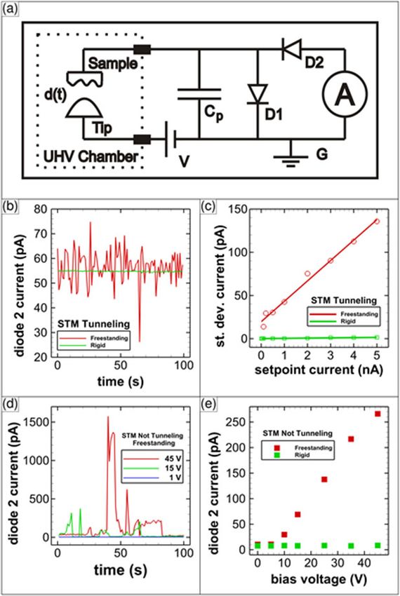
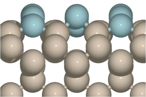
NOTTINGHAM

Encapsulation of Metal Nanoparticles Near the Surface of Graphite
 Ann Lii-Rosales1,2* and Patricia A. Thiel1,2,3
 1
 The Ames Laboratory–USDOE, Ames, IA 50011, USA
 2
 Department of Chemistry, Iowa State University, Ames, IA 50011, USA
 3
 Department of Materials Science and Engineering, Iowa State University, Ames, IA 50011, USA

 *Nottingham Contestant

 Email: ylii@iastate.edu

 In this study we investigate the phenomenon of metal encapsulation near the surface of a layered
material, graphite, by combining scanning tunneling microscopy (STM), X-ray photoelectron spectroscopy
(XPS), and density functional theory (DFT) calculations. We develop a synthetic strategy that can
encapsulate metals when two conditions are met: (i) defects must be generated on the graphite surface, via
argon ion bombardment, and (ii) the graphite surface with ion-induced defects must be held at elevated
temperature for metal deposition from the vapor phase.

 Our synthetic strategy is effective for a variety of metals,
including rare earth metals Dy and Gd, transition and noble metals Cu,
Fe, Ru and Pt. Characterization via STM shows that the metals form
nanocrystalline islands composed of multiple metal layers. STM also
reveals atomic features on top of the islands: A contiguous, carpet-like
carbon lattice that drapes over the islands, which serves as firm evidence
of encapsulation. Figure 1 showcases encapsulated Cu islands. In
addition, XPS shows that the metal islands are metallic. Furthermore, Ru
islands remain metallic even after long-term exposure to ambient
conditions.

 Despite the strategy’s considerable robustness, it is ineffective Figure 1. STM image of
for Ag and Au. This is initially a prediction drawn from DFT results and encapsulated Cu islands. Inset
then later attested by experiments. We find that the relative energetics of
 shows a schematic of a metal
a single metal atom – adsorbed on the graphite surface vs. encapsulated
between graphene layers – are of key significance. This shows that
 cluster embedded beneath a
predicative capability can develop when coupling theoretical insights graphene overlayer. Image
with the synthetic strategy. size is 750 nm x 750 nm.

 Our work opens up the possibility to fabricate arrays of nanoscale heat sinks (Cu) or nanomagnets
(Fe), while the metals are protected from oxidation. We also envision that our synthetic strategy can be
extended to other layered materials to create interesting nanostructures encapsulated near their surface.

 N.3
NOTTINGHAM

 Well-Defined Pt/CeO2 catalysts synthesized by Atomic Layer
 Deposition
 Bochuan Song1* and Helena E. Hagelin Weaver1

 *Nottingham Contestant
 1
 Chemical Engineering, University of Florida, Gainesville, FL 32611, USA

 Email: bsong94@ufl.edu

 Using Atomic Layer Deposition (ALD) to synthesize heterogeneous catalysts with atomic level
precision has gained increasing interest in recent years. In our laboratory we have synthesized well-defined
heterogeneous catalysts by depositing Pt onto various CeO2 nanoshapes using ALD. The benefit of using
CeO2 nanoshapes is that the surface facets of each shape are well defined, as the CeO2 octahedra have (111)
surface terminations, the CeO2 cubes expose (100) surface facets, while the CeO2 rods consist of (100) and
(110) surface facets. Therefore, this allows us to determine the influence of the support oxide surface
structure on the active metal and ultimately on the probe reactions. These catalysts can also facilitate
identifying structure-activity relationships, as well as comparisons to theoretical studies and ultra-high
vacuum surface science studies on single crystals. By using ALD during catalyst synthesis we obtain better
control over the active metal deposition, compared with conventional catalyst preparation techniques. We
have shown that by tuning the ALD conditions, such as precursor temperature, deposition temperature and
dose length, we can carefully control the Pt loading on the CeO2 nanoshapes. The Pt loading and the CeO2
surface facet have significant effects on the CO oxidation, which we have used as our initial probe reaction.

 N.4
NOTTINGHAM

 Normal-Stress-Induced Mechanochemical Decomposition
 of Methyl Thiolates on Cu(100)

 A. M. Boscoboini1* and W. T. Tysoe1
 *Nottingham Contestant
 1
 Department of Chemistry & Biochemistry, University of Wisconsin Milwaukee,
 3210 N Cramer St, Milwaukee, WI 5321, USA

 Email: boscobo2@uwm.edu

Improving lubricant additives and identifying how they react at surfaces is important for reducing
macroscopic and microscopic friction (e.g. cars and micromachines)[1]. The mechanically induced rate
of a chemical reaction is described by the Bell model [2] where the rate constant for a reaction under
an applied stress is given by 0exp Δ ‡/ BT , here B is the Boltzmann constant, 0 is the
reaction rate in the absence of stress, Δ ‡ is known as the activation volume and is the absolute
temperature. While exponential increases in reaction rates with stress have been reported, there are
currently no quantitative measurements. This is
addressed by using contact-mode AFM to measure
the kinetics of mechanochemically induced C-S bond
cleavage methyl thiolate on Cu(100) in ultrahigh
vacuum. The experimental rate of methyl thiolate
decomposition increases exponentially with stress
(Fig. 1, ■) with an activation volume of 37.6 ± 0.9
Å3, but this value does not agree quantitatively with
the predictions of the Bell model (‒‒). However, the
results of DFT calculations [3] of the energy barrier
for methyl thiolate decomposition under the
influence of a normal force (‒‒) provide excellent
agreement with experiment. An analysis of the results
indicates that the effect of a normal stress is to both Fig. 1. Comparison of experiment and theory.
destabilize the initial state and to lower the energy of Pressure-induced methyl thiolate decomposition
the transition state. These results will enable the on Cu(100) in ultrahigh vacuum.
description of mechanochemical reactions to be
placed on a firm theoretical footing that will ultimately enable them to be quantitatively predicted.

References:
[1] O.M. Braun, A.G. Naumovets, Surf. Sci. Rep. 60, 79–158 (2006).
[2] G. I. Bell, Cell Biophys. 1, 133 (1979).
[3] H. L. Adams, UWM Theses/Dissertations. 1566, 145, (2017).

 N.5
NOTTINGHAM

 Symmetry Considerations for Interactions on MoS2
 Prescott E. Evans,1* and Peter A. Dowben1

 *Nottingham Contestant

 1
 Department of Physics and Astronomy, University of Nebraska-Lincoln, 855 N 16th St., Lincoln,
 Nebraska 68588-0299, United States.

 Email: prescott.evans@huskers.unl.edu

 MoS2 is a well-recognized 2D material and catalyst. From extensive studies of the electronic band
structure, it is now understood that, like the other transition metal dichalcogenides [1,2], the electronic
structure of monolayer MoS2 differs from bulk MoS2(0001). Furthermore, other electronic band structure
studies have found marked differences between the theoretical surface symmetry of the Brillouin zone and
an observed retention of high symmetry in MoS2(0001) band structure [3]. The massive role of symmetry
in the adsorbate-MoS2 interaction cannot be underscored enough, and is another experimental verification
of the retention of local symmetry in the electronic structure. The role of adsorbate frontier orbital symmetry
and preservation of MoS2 surface symmetry has been demonstrated by comparing the adsorption of the
isomers of diiodobenzene on MoS2 [4]. Experiments indicate that the adsorption of 1,3-diiodobenzene on
MoS2(0001) is much more facile compared to other isomers, contrary to negligible differences in calculated
adsorption energies and electron affinities. The combination of density functional theory and experiment
highlights frontier orbital symmetry as key to diiodobenzene adsorption on MoS2(0001). The surface
symmetry of MoS2 also plays a role in defect creation at the MoS2(0001) surface, wherein defects and
symmetry have a hand in catalytic activity and application. Surface reactions on MoS2 can be enhanced by
defects [5, 6], but we have shown that surface reactions can also create defects, as in the example of
methanol to methoxy reactions [7]. The difference in electronic structure and application of the monolayer
from bulk is emphasized by the ability to anneal out defects for bulk MoS2(0001) [8], which will persist for
the monolayer. From experiment it is clear moving forward theory must include further considerations of
symmetry such as frontier orbital symmetry as well as monolayer and bulk considerations such as band
bending, and interface charge transfer to gain more accurate insight into reaction mechanisms on MoS2.

References:
[1] I. Tanabe et al., J. Phys. Conden. Matter 28 (2016) 345503
[2] I. Tanabe, et al., Applied Physics Letters 108 (2016) 252103
[3] T. Komesu, et al., J. Phys.: Condens. Matter 26 (2014) 455501
[4] P. E. Evans, et al., Chem. Comm. (2019) submitted
[5] T. B. Rawal, D. Le, T. S. Rahman, T. S., J. Phys. Chem. C 121 (2017) 7282-7293.
[6] T. B. Rawal, D. Le, T. S. Rahman, J. Physics: Cond. Matter 29 (2017) 415201.
[7] P. E. Evans, et al., J. Phys. Chem. C 122 (2018) 10042-10049
[8] P. E. Evans, H. K. Jeong, P. A. Dowben, MRS Advances (2018); doi: 10.1557/adv.2018.634

 N.6
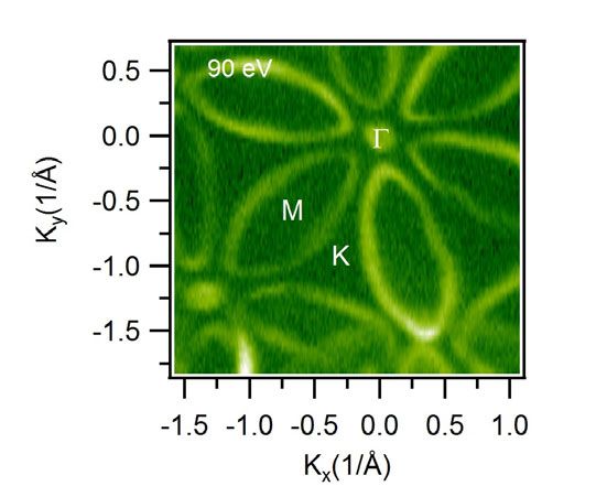
NOTTINGHAM

 Distinct multiple fermionic states in a single topological metal
 M. Mofazzel Hosen1, and M. Neupane1
 1
 Department of Physics, University of Central Florida, Orlando, FL 32816, USA

 Email: dolar.kabir@knights.ucf.edu

Among the quantum materials that have recently gained interest are the
topological insulators, wherein symmetry-protected surface states cross in
reciprocal space, and the Dirac nodal-line semimetals, where bulk bands
touch along a line in k-space. However, the existence of multiple fermion
phases in a single material has not been verified yet. Using angle-resolved
photoemission spectroscopy (ARPES) and first-principles electronic
structure calculations, we systematically study the metallic material
Hf2Te2P and discover properties, which are unique in a single topological
quantum material. We experimentally observe weak topological insulator
surface states and our calculations suggest additional strong topological
insulator surface states. Our first-principles calculations reveal a one-
dimensional Dirac crossing-the surface Dirac-node arc-along a high- Fig. 1. ARPES measured
symmetry direction which is confirmed by our ARPES measurements. Fermi surface at a photon
This novel state originates from the surface bands of a weak topological energy of 90 eV. High
insulator and is therefore distinct from the well-known Fermi arcs in symmetry points are noted in
semimetals. Our discovery opens a unique platform to study the interplay the plots. Here, Gamma is the
between various novel topological states. center of the Brillouin zone
 and K is the corner and M is
 the mid-point between
Ref.
 adjacent corners [1].
[1] M. M. Hosen, et al., Nat. Commun. 9, 3002 (2018).

 N.7
NOTTINGHAM

Oxidation of Semiconductors and Semimetals by Supersonic Beams
 of O2 with Scanning Tunneling Microscopy Visualization
 Ross Edel* and Steven J. Sibener

 *Nottingham Contestant

Department of Chemistry, University of Chicago, 5741 S Drexel Ave, Chicago, IL, 60637, USA

 Email: redel@uchicago.edu

Our research examines the oxidation of semiconductor and semimetal surfaces using a novel, one-
of-a-kind instrument that combines a supersonic molecular beam with an in-line scanning
tunneling microscope (STM) in ultra-high vacuum. This new approach to surface reaction
dynamics provides spatiotemporal information on surface oxidation over nanoscopic and
mesoscopic length scales. We have uncovered the kinetic and morphological effects of oxidation
conditions on three technologically relevant surfaces: Si(111)-7×7, highly oriented pyrolytic
graphite (HOPG), and GaAs(110). A complete understanding of the oxidation mechanism of these
surfaces is critical due to their technological applications and roles as model systems. Samples
were exposed to O2 with kinetic energies from 0.4-1.2 eV and impingement angles 0-45° from
normal, with STM characterization between exposures. In some cases, we were able to monitor
the evolution of specific features by revisiting the same nanoscopic locations. Our study of
Si(111)-7×7 revealed two oxidation channels, leading to the formation of dark and bright reacted
sites. The dark sites dominated the surface and exhibited almost no site selectivity while the bright
sites preferred the corner sites of the 7×7 unit cell. Our observations suggest that two adsorption
pathways, trapping-mediated and direct chemisorption, occur simultaneously. On HOPG, we
found that different oxygen energies, incident angles, and surface temperatures produce
morphologically distinct etching features: Anisotropic channels, circular pits, and hexagonal pits.
Reaction probability increased with beam energy and demonstrated non-Arrhenius behavior with
respect to surface temperature, peaking at around 1375 K. Finally, oxidation of GaAs(110) was
found to proceed by two morphologically distinct, competing mechanisms: a homogeneous
process leading to layer-by-layer oxide growth, and a heterogeneous process with oxide islands
nucleating from surface defects. The rates of both mechanisms change with O2 kinetic energy,
with homogeneous oxidation dominating at lower energies (
NOTTINGHAM Growth and Characterization of Large-Area Ultrathin InSe Hadallia Bergeron1* and Mark C. Hersam2 *Nottingham Contestant 1 Department of Materials Science and Engineering, Northwestern University, Evanston, Illinois 60208, USA 2 Department of Materials Science and Engineering, Department of Chemistry, and Department of Electrical Engineering and Computer Science, Northwestern University, Evanston, Illinois 60208, USA Email: hadalliabergeron2014@u.northwestern.edu The lack of large-area synthesis methods for emerging 2D materials presents a significant challenge for nanoelectronic devices and systems. In particular, InSe is a semiconducting van der Waals (vdW) material that possesses exceptional band-gap tunability as a function of thickness in the ultrathin limit. Despite its desirable electronic properties, InSe is a relatively under-investigated 2D material, primarily due to the fact that high-quality samples have only been achieved via mechanical exfoliation as opposed to large-area thin-film growth. While many of the extensively studied and synthesized vdW 2D material systems have relatively simple phase diagrams (e.g., MoS2), the complex phase diagram for InSe has hindered the development of large-area thin films, thus motivating more fundamental studies aimed at characterizing and understanding growth mechanisms. Towards that end, we use in operando X-ray diffraction (XRD) and diverse surface characterization techniques (e.g., X-ray photoelectron spectroscopy, Raman spectroscopy, atomic force microscopy, transmission electron microscopy, and selected area electron diffraction) to study the structural and compositional evolution of ultrathin InSe films grown by pulsed laser deposition and subsequent vacuum thermal annealing. The complexity of the indium– selenium phase diagram manifests itself during annealing, with the film initially passing through a partial In4Se3 crystallization at low temperatures and ultimately degrading into an In2Se3 matrix at higher temperatures. However, by monitoring all temperatures in operando, this methodology Fig. 1. in operando XRD of a PLD InSe efficiently determined that InSe films with no detectable thin-films on 300 nm SiO2 as a function impurity phases can be achieved at post-deposition annealing of annealing temperature, with the as- temperatures between 350 C and 450 C (Fig. 1). The deposited amorphous film in black. Peaks resulting InSe films possess high uniformity in stoichiometry indexed as InSe are denoted by the black and crystallinity over large areas with controlled thickness, dashed lines. thus providing an ultrathin InSe synthesis technique that is generalizable to a wide range of substrates suitable for nanoelectronic applications. N.9
NOTTINGHAM

 Borophene and its Functionalization
 Xiaolong Liu1* and Mark C. Hersam1,2

 *Nottingham Contestant
 (current affiliation: Physics, Cornell University)

 1
 Applied Physics Graduate Program, Northwestern University, 2220 Campus Drive, Evanston,
 Illinois 60208-3108, USA
 2
 Department of Materials Science and Engineering, Department of Chemistry, Department of
 Medicine, Department of Electrical Engineering and Computer Science, Northwestern
 University, 2220 Campus Drive, Evanston, Illinois 60208-3108, USA

 Email: xiaolongliu2013@u.northwestern.edu

Following theoretical predictions, 2D boron (i.e., borophene) was experimentally realized in late 2015,
showing intriguing properties such as high in-plane anisotropy. As a synthetic 2D material on Ag(111)
substrates, its structural properties such as intrinsic defects and polymorphs cannot be deduced from bulk
boron. In particular, the complex lattice structures of borophene polymorphs remain to be experimentally
verified. Given the dominant role of structural defects in 2D systems and the knowledge gap in borophene
surface chemistry, we perform atomically-resolved study of borophene structures and chemical
functionalization using ultra-high vacuum scanning tunneling microscopy (STM) and non-contact atomic
force microscopy (nc-AFM). Borophene phases corresponding to the v1/6 and v1/5 models are found to
coexist and intermix periodically in the form of line defects, giving rise to new borophene phases. To
overcome the imaging ambiguity of conventional STM, we use CO-functionalized AFM to geometrically
reveal features corresponding to B-B covalent bonds and assemble a growth phase diagram of borophene,
confirming the v1/5 and v1/6 borophene models as the unifying structures for all observed borophene
polymorphs even in newly discovered incommensurate phases. Towards the realization of borophene-based
nanoelectronics, we chemically functionalize borophene with self-assembled organic molecules, resulting
in the spontaneous formation of electronically abrupt lateral heterostructures that is further explored as a
platform for covalent chemistry. Overall, our work informs both fundamental studies of borophene material
properties and emerging efforts in realizing borophene-based nanoelectronics.

 N.10
ORAL

 Sulfur-Metal Interactions on Ag(100) and Ag(110) at Low
 Coverages
 Peter M. Spurgeon,1 Da-Jiang Liu,2 Junepyo Oh,3 Yousoo Kim,3 and Patricia A. Thiel1,2,4
 1
 Department of Chemistry, Iowa State University, Ames, IA, 50010, USA
 2
 Ames Laboratory of the USDOE, Ames, IA, 20010, USA
 3
 RIKEN Surface and Interface Science Laboratory, Wako, Saitama 351-0198, Japan
 4
 Department of Materials Science and Engineering, Iowa State University, Ames, IA, 50010, USA
 Email: peterms@iastate.edu

Coinage metals (Cu, Ag, Au) are of interest due to their catalytic and plasmonic properties, especially
when they are in the form of nanoparticles. Sulfur is an important adsorbate on these metals because
sulfur is known to enhance mass transport of coinage metal nanoparticles. Recent studies of chemisorbed
sulfur on the coinage metals have shown that even at extremely low sulfur coverages, well below 0.10
monolayers, indigenous metal atoms can react to from complexes on some surfaces. (A complex is an
isolated species consisting of metal and sulfur atoms, and with well-defined shape, size, and
stoichiometry.) In other systems, isolated adatoms or extended reconstructions are observed. For example,
sulfur and copper form a heart-shaped Cu2S3 complex on Cu(111)1, whereas sulfur forms only isolated
adatoms on Au(111)2.
 Here, we report a study of sulfur on Ag(110) and Ag(100) at multiple coverages. The main
experimental technique is low-temperature scanning tunneling microscopy (LT-STM). At low coverages
(~0.02 monolayer) we observe that sulfur forms isolated adatoms on Ag(110), but at higher coverages
(~0.25 monolayer) there is evidence of AgS2 complexes coexisting with S adatoms. For sulfur on Ag(100),
we observe that sulfur forms isolated adatoms within our entire experimental coverage range (0.01 - 0.1
monolayer).

References:
[1] H. Walen, D. -J. Liu, J. Oh, H. Lim, J. W. Evans, C. M. Aikens, Y. Kim, and P. A. Thiel. "Cu2S3complex
on Cu(111) as a candidate for mass transport enhancement". Phys. Rev. B 91, 045426 (2015)
[2] H. Walen, D. -J. Liu, J. Oh, H. Lim, J. W. Evans, Y. Kim, and P. A. Thiel. "Self-organization of S
adatoms on Au(111): Rt.3R30 rows at low coverage" J. Chem. Phys. 143 014704 (2015).

 Fig. 1. STM image of AgS2 complexes
 and S adatoms at 0.25 ML. Image is 10
 x10 nm2.

 O.1
ORAL

Defect-laden Hexagonal Boron Nitride for the Reduction of Carbon
 Dioxide
 Richard G. Blair1, Katerina L. Chagoya2, 1, Talat S. Rahman3

 1
 Florida Space Institute, University of Central Florida, 12354 Research Parkway, Suite 214
 Orlando, FL 32826-2933
 2
 Mechanical Engineering, University of Central Florida, 12760 Pegasus Drive
 Orlando, FL 32828
3
 Physics, University of Central Florida, 4000 Central Florida Blvd. - PSB 430 Orlando, FL 32816-2385

 Email: richard.blair@ucf.edu

 Heterogeneous catalysis is often most rapid on surface discontinuities
such as grain boundaries or steps. Much work has gone into growing
non-equilibrium structures such as nanostructures with specific shapes
to control surface discontinuities and enhances catalytic pathways.
Improved catalysis is realized by controlling the localized molecular
orbital structure, which can vary significantly from the bulk material.
Catalytic activity can be introduced into surfaces previously thought of
as inert through the introduction of discontinuities in the form of defects.
Defects can be introduced through mechanical processing. Catalyst
surfaces undergo plastic deformation when processed with forces Fig. 1. A nitrogen vacancy
beyond the ultimate tensile strength of the bulk material producing and (VN) in the hexagonal boron
mobilizing non-equilibrium defect structures. In highly defect-laded nitride sheet has a localized
boron nitride surfaces (dh-BN), these defect structures can be exploited electronic structure that
for the hydrogenation of olefins[1] and the reduction of carbon dioxide. facilitates catalysis. Defect-
Controlling the reaction temperature allows realization of formic acid or free h-BN surfaces are not
methanol. Application of a low energy, heterogeneous route to CO2 active.
reduction that can be intensified using traditional chemical engineering
principles will reduce emissions and produce a profitable product.

References:
[1] D. J. Nash, D. T. Restrepo, N. S. Parra, K. E. Giesler, R. A. Penabade, M. Aminpour, et al.,
 ACS Omega, 1,(2016).

 O.2
You can also read