Designs of Area and Power Efficient Carry Select Adders:A Review - IJARECE
←
→
Page content transcription
If your browser does not render page correctly, please read the page content below
ISSN: 2278 – 909X
             International Journal of Advanced Research in Electronics and Communication Engineering (IJARECE)
                                                                                  Volume 7, Issue 3, March 2018

              Designs of Area and Power Efficient Carry
                      Select Adders:A Review
                                                     Shalini Singh, Sunita Malik
                                               Department of Electronics and Communication
                                        Deenbandhu Chhotu Ram University of Science & Technology
                                                          Murthal, Sonipat, India
        s

Abstract-Adders play a very crucial role in arithmetic and data         Govind Prasad, V Shiva Prasad Nayak, et.al [9]:        have
path application. For high performance processors, there needs          proposed carry select adder designs that are area and power
to be a power, delay and area efficient adders. In this paper, the      efficient. This has been proposed through Cadence Virtuoso
different types of carry select adders are explained.The                tools for 90-nm CMOS process Technology.
conventional carry select adder, advanced carry select
adder,Carry select adder based on D-Latch and the CSLA                  Abhiram T, Ashwin T, et.al[11]: The design architectures of
using Gate Diffusion input, all these architectures are compared        CSLA are developed using Verilog –HDL and the different
based on area and power consumption. A comparison is done               parameters like area, power and
which shows the comparison between the different parameters             time have been surveyed by using Synopsys design
of carry select adders. The basic purpose behind comparing the
                                                                        compiler tool for 90nm technology.
adders is to obtain a power and area efficient carry select
                                                                        Shivani Parmar and Kirat Pal Singh [6]:They have proposed
adder.
                                                                        carry select adder designs that are area and power efficient.
                                                                        They have made use of Xilinx Spartan-3 device to synthesize
Keywords:RCA (Ripple Carry Adder); GDI (Gate Diffusion                  the design at 90nm process technology.
Input) technique; CSLA (Carry Select Adder (CSLA)); BEC
(Binary Excess Code); Cin (Carry Input).                                Raghava Katreepalli and Themistoklis Haniotakis[12]: They
                                                                        have proposed that for designing highly efficient processing
            I. INTRODUCTION                                             units, there needs to be highly efficient adders (high speed)
                                                                        having low power utilizations.They have validated the
                                                                        proposed design by making use of adder circuits of 16 and 32
 Factors that affects the performance of the signal processor           bits in 45nm CMOS process technology.
 are power and speed. In this paper, we have described
 different adders based on the area, power, speed and                             III. DIFFERENT TYPES OF ADDER
 delay.Speed and delay are affected by the carry propagated
 at the previous stage. The current stage sum depends on the
                                                                         A) Conventional Carry Select Adder (CSLA)
 previous stage carry and thus the sum cannot be calculated
 until the previous stage carry is received at the current
 stage.Hence it affects the speed and creates delay.                     CSLA is an abbreviation used carry select adder. We all are
                                                                         known to the fact that adders are highly utilized in data
The rest of the paper is organized such that section II consists         processors for performing arithmetic functions. And CSLA
of literature review, section III comprises of different types           is one of the fastest adders which is used for performing
of adders with their block diagrams. There is also a section             arithmetic operations of a data processor and signal
IV named as applications of adders respectively. The results             processor.
and conclusionsis given in section V in which a comparison
is given between different designs of CSLA adders based on               In Ripple Carry Adders, we faced the problem of carry
the parameters like area (number of transistors) and power.             propagation delay. The sum of the current stage had to wait
                                                                        for the previous stage to be processed further. This was time
II. LITERATURE REVIEW                                                   consuming and was increasing the delay which was affecting
                                                                        the speed and the performance of the system.Hence, we are
Pavan Kumar, M.O.V, Kiran. [1]:In this paper, they have                 using dual ripple carry adders in the architecture of CSLA.
discussed adders on three different frequencies.In this study,          In this review, the fig.1 shows the architecture of a 4bit
various adders are compared by making use of cadence
                                                                        ripple carry adder which consists of full adders and a
virtuoso tool for 45-nm CMOS technology.

                                                                                                                         221
                                                  All Rights Reserved © 2018 IJARECE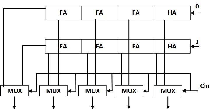
ISSN: 2278 – 909X
                        International Journal of Advanced Research in Electronics and Communication Engineering (IJARECE)
                                                                                                    Volume 7, Issue 3, March 2018
    multiplexer. The sum from the adders is sent to the             In advanced CSLA, the architecture is slightly different from
    multiplexer.                                                    the conventional CSLA.
    In the architecture of CSLA, we have dual ripple carry
    adders: one is used to calculate sum for carry `0` and another  In the conventional CSLA, we have two RCA, one with Cin
    is used to calculate the sum for carry `1`.And Multiplexer is   = `0 ` and another with Cin = `1`.In advanced CSLA, the
    used to select the output based on the actual carry.If the      RCA with Cin =`1` is replaced by BEC (Binary Excess
    actual carry is `0`, the multiplexer takes the output of RCA    Code). This is done to make the architecture area efficient
    using carry `0` for computation and vice –versa.                and to reduce the power consumption. In the architecture of
                                                                    advanced CSLA, the number of EX-OR gates is reduced.
                                                                    The final output is again selected by the actual carry which
                                                                    acts as the select line to the multiplexer.

                                                                       The internal architecture of a 4 bit BEC is given in the fig.3
                                                                       and the structured diagram of Advanced CSLA is given in
                                                                       the fig.4.

        Fig.1 Ripple carry adder

    The fig.2 shows the block diagram of a conventional CSLA.

                                                                       Fig.3: BEC 4 – bit

l

    Fig. 2: Conventional Carry Select Adder

    The block diagram given below shows that, it is understood
    that each bit is computed twice. The incoming carry is sent to
    the multiplexer and acts as a select line for it. As we can see
    in this architecture, first RCA is assuming the carry is `0` and
    secondly RCA is assuming that the carry is `1`. And
    performs their respective computations. Their respective           Fig.4: Advanced CSLA
    sums and carries are received by the multiplexer. Depending
    on the incoming carry, the corresponding sum and carry are         C) Carry Select Adder using D-Latch
    studied.
    Advantage of CSLA is that it reduces the carry propagation         For reducing the power consumed by the conventional carry
    delay and the disadvantage is that it is using more area since     select adder, the carry select adder is combined with D-
    in the architecture there are dual ripple carry adders.            Latch.

    B) Advanced CSLA

                                                                                                                                   222
                                                    All Rights Reserved © 2018 IJARECE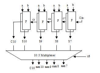
ISSN: 2278 – 909X
                    International Journal of Advanced Research in Electronics and Communication Engineering (IJARECE)
                                                                                         Volume 7, Issue 3, March 2018
In this architecture, d-latch is replacing one of the 2 RCA`s
used in the conventional carry select adder.Here, if the
enable input is 1, dlatch`s output is similar as its input else
the previous output is stored itself. In D-latch carry select
adder, there is requirement of only one ripple carry adder and
another one is replaced by D-latch circuit. The outputs of D –
Latch are regularly influenced by the inputs, every time the
enable (E) signal is used.

The fig.5 shows the D-Latch circuit. The fig.6 shows the
circuit diagram of CSLA using D-Latch.

In the following circuit of carry select adder using D-Latch,
the multiplexer is used to give the final output. The sum and
the carry corresponding to the carry in are selected by using
multiplexer,when the carry input is provided to multiplexer.

                                                                              Fig.6:CSLA using D-Latch

                                                                  D) Carry Select Adder Using GDI

                                                                  In this GDI based CSLA, we have replaced the conventional
                                                                  CSLA and CSLA based on D-Latch for reducing the power
                                                                  consumption. The resultant circuit after the replacement is
                                                                  providing higher and better performance. The table I is the
                                                                  truth table of a full adder.
Fig. 5: D-Latch circuit diagram
                                                                  Look at the truth table of full adder given below.
D-Latch is used to store 1-bit information from RCA,
whenever the carry input is 1.But when the carry input is 0,
                                                                                TABLE I: Full Adder Truth Table
the computation takes place in RCA and D-Latch gets
disabled.

The fig.6 shows the circuit diagram of carry select adder
using D-Latch.

                                                                  In this, when the Cin =`0`,the carry is following AND
                                                                  operation and for Cin =`1`,it follows OR operation.

                                                                                                                          223
                                               All Rights Reserved © 2018 IJARECE
ISSN: 2278 – 909X
International Journal of Advanced Research in Electronics and Communication Engineering (IJARECE)
Volume 7, Issue 3, March 2018
In this GDI based CSLA,we will use the above in a circuit
form with use of XOR, AND,OR and XNOR gates ,using
two (2:1) multiplexers for the selection of appropriate sum
and carry .This reduces the delay .The figure 7 shows the
proposed adder circuit using the GDI technique.
Fig.8: Basic GDI Cell
Now, we have the following table, where we can see the
Fig.7: Proposed circuit diagram using GDI number of transistors used in GDI and the number of
Technique transistors used in CMOS for any particular logical
operation. The table III shows the number of transistors used.
The circuits that uses GDI cell are less complex. The number
of transistors and voltage swing is also reduced. Since the TABLE II: Functions Implementation
number of transistors is less, the carry propagation delay is
minimized.
For the implementation of any logic function,we generally
require 2 transistors. The only element of this circuit is that
the voltage swing is reduced. We can rectify the issue by
making use of full swing GDI.The technique is an alternative
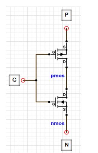
to CMOS design.GDI structure consists of 3 parts,namely, P,
G and N. P is source (drain of PMOS),N is source (drain of
NMOS) and G is common gate input to both the NMOS and
PMOS. In a basic GDI cell,we have the PMOS connected to
VDD and NMOS connected to GND. The figure 8 shows a
basic GDI cell.We can perform the following functions using
a GDI cell, those given in table below. The table II shows the
functions implementation table.
224
All Rights Reserved © 2018 IJARECEISSN: 2278 – 909X
International Journal of Advanced Research in Electronics and Communication Engineering (IJARECE)
Volume 7, Issue 3, March 2018
TABLE III: Number of Transistors used IV. APPLICATIONS OF ADDER
The most basic arithmetic operation is addition. It is the
most basic and highly used operation in the midst of sets of
real time digital signal processors ranging from application
specific digital signal processors to general purpose
processors. The several applications of adders are as
follows:
They are used to make on-chip libraries.
They are configurable hence can be configured
according to the complexities in arithmetic and
numeric computations.
In processing and computing devices, they are
used as the arithmetic logic unit.
Adders can be used to reduce the circuits
complexity.
They are used at networking sides.
Adders are used at DSP Oriented Systems.
They are used in different types of processors like
snapdragon, Exynous and in Intel Pentium for
CPU part.
CPU consist of ALU (Arithmetic and Logic unit)
for performing operations like add, subtract,
multiply etc.
The microprocessors have them in their data paths.
They are used in different circuits like high speed
integrated circuits, digital signal processing and
application specific ICs.
They are also found in Multiply Accumulate
Structures (MAC).
They form the exclusive units for integer and
floating points.
They form the basic building blocks for a DSP
processor.
In controllers, they are used for flag generation
The number of transistors used in GDI is very less as
and address calculations purposes.
compared to the number of transistors used in CMOS design.
V.COMPARISION TABLE
Since the number of transistors is reduced hence the power
The various types of carry select adders have been
consumption is also reduced. The problem of reduction of
compared based on the size of the adders as 1,8,16,32 bits.
voltage swing can be rectified by making use of 2 CMOS
The comparative analysis of the various design
inverters. Due to this, there will be a slight increase in power.
architectures of carry select adders are given in the
GDI technique has provided us with an adder that can
following table.
perform operations faster and with a reduced no of
transistors.
225
All Rights Reserved © 2018 IJARECEISSN: 2278 – 909X
International Journal of Advanced Research in Electronics and Communication Engineering (IJARECE)
Volume 7, Issue 3, March 2018
TABLE IV: Comparison Table 3. Bernd Becker, Rolf Drechsler, Rolf Krieger, Sudhakar M.
Reddy, “A Fast Optimal Robust Path Delay Fault Testable
Type of Adder Power No. of
Transistors Adder”, IEEE ,1996.
Conventional CSLA
4. A. T. M. Shajiqul Khalid, “A FAST OPTIMAL CMOS
(1 Bit) 0.178uw 28 FULL ADDER “, IEEE, 1997
(8 Bit) 128uw 368 5. Er. Aradhana Raju, Richi Patnaik, Ritto Kurian Babu,
PurabiMahato, “Parallel Prefix Adders- A Comparative
(16 Bit) 34.325uw 497 Study for Fastest Response”
(32 Bit) 50.295uw 954 6. Shivani Parmar, Kirat Pal Singh,” Design of high speed
Advanced CSLA hybrid carry select adder”, IEEE ,2012
(16 Bit) 29.429uw 462
7. Dayu Wang, Xiaoping Cui, Xiajing Wang, “Optimized
design of Parallel Prefix Ling Adder”, IEEE ,2011
(32 Bit) 45.083uw 897
D-Latch Based CSLA
8. David H. K. Hoe, Chris Martinez and Sri
(1 Bit) 11.57uw 76 JyothsnaVundavalli, “Design and Characterization of
Parallel Prefix Adders using FPGAs”, IEEE, 2011.
(8 Bit) 11.76uw 440
9. GovindPrasad, SSachin, K Lava Kumar, Soma Sai
Kumar, “Area and Power Efficient Carry- Select Adder”,
GDI Based CSLA IEEE, 2016.
(1 Bit) 0.102 14 10. S.A.H Ejtahad, M.B. Ghaznavi-Ghoushchi, “Design and
implementation of power and area optimized reconfigurable
(8 Bit) 7.7 112 superset parallel prefix adder”, IEEE ,2016.
VI. RESULT AND CONCLUSION 11. Abhiram T, Ashwin T, Sivaprasad B, Aakash S, Anita
J.P, “Modified Carry Select Adder for Power and Area
In this paper, they have studied various design architectures
Reduction”, IEEE, 2017.
of carry select adders. Firstly, they have studied the
architectures of a conventional CSLA and came to a
12. Raghava Katreepalli and ThemistoklisHaniotakis, “High
conclusion that it consumes more area and power. Then they
Speed Power Efficient Carry Select Adder Design”,
reduced area and power consumption but the delay was
IEEE,2017
higher than they studied the CSA based on D-Latch and got a
circuit with reduced power and area which was the main
purpose behind its designing. In the CSLA based on GDI,
they finally got a faster adder with less number of transistors.
VII. REFRERNCES
1. Pavan Kumar, Kiran.M,” DESIGN OF OPTIMAL FAST
ADDER”, IEEE ,2013
2. Sabyasachi Das, Sunil p. Khatri, “Generation of the
Optimal Bit-Width Topology of the Fast Hybrid Adder in a
Parallel Multiplier” IEEE ,2007
226
All Rights Reserved © 2018 IJARECEYou can also read