Deep Channel Analysis for High-Speed Interconnect Solutions - CADFEM
←
→
Page content transcription
If your browser does not render page correctly, please read the page content below
HIGH-SPEED
ELECTRONICS
Deep Channel Analysis
for High-Speed
Interconnect Solutions
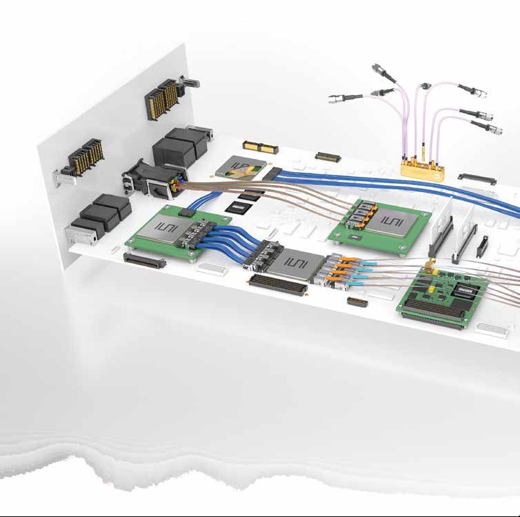
Data center servers, storage and networking equipment communicate over
copper and optical cable assemblies joined by ever-faster connectors.
Samtec leverages a comprehensive suite of simulation software from
ANSYS to design and optimize next-generation, high-performance
interconnect solutions across the entire signal channel.
By Scott McMorrow, CTO, Signal Integrity Group, and
Matt Burns, Product Marketing Manager,
Samtec, Inc., New Albany, USA
14 ANSYS ADVANTAGE ISSUE 3 | 2017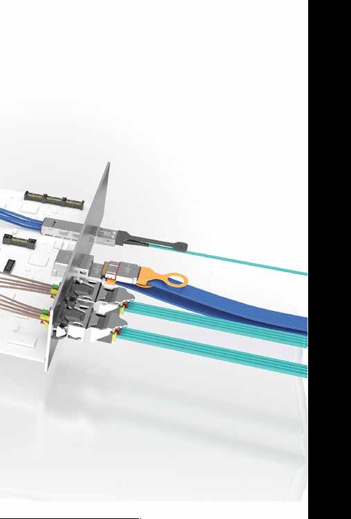
“The flexibility of the state-of the-art 3-D full-wave solvers in
       ANSYS HFSS allows Samtec to target subcomponent and system
                     modeling. Engineers can perform large connector
                     modeling for customer system simulations and
                                  extract large sections of packages for deep
                                           analysis of potential issues.           ”

Data. Data. Data. Consumers demand real-time              and beyond. Routing high-speed signals throughout a
access to personal and professional data no matter        system presents many design challenges. While legacy
where they are or what the time of day. Twenty-first–     design decisions were made at the component level,
century consumers and workers are untethered, so          engineering 28 Gbps systems requires a deep analysis
mobile data is expected. At the end of 2016, global       of the entire channel from IC to IC via packages, PCBs
mobile data traffic reached 7.2 exabytes per month        and interconnect solutions. How does Samtec — the
(an exabyte is one billion gigabytes). That number will   service leader in the electronic interconnect industry
exceed 49 exabytes per                                                                  with full-channel system
month by 2021 [1].                                                                      support from the IC to
    The demands of easily                                                               the board and beyond —
accessible mobile data via                                                              support deep analysis
cellular and fixed networks                                                             throughout the high-speed
(via Wi-Fi and low-power                                                                channel?
cellular base stations
called femtocells) places                                                             Designing a High-Speed
increasing demand on                                                                  Signal Channel
data centers and backbone                                                             Next-generation,
networks. Data center                                                                 multigigabit-per-second
equipment — servers,                                                                  designs require a holistic
storage, communications                                                               approach for the signal
and networking — are constantly upgraded to support       channel path. Developers cannot focus on just one
higher data rates.                                        component, but must analyze and optimize the
    Data center equipment OEMs must keep up with          interaction of all components across the entire channel.
demand. Current-generation solutions typically               Each component in a channel has design variables
support data rates of 10 Gbps to 15 Gbps. Next-           that affect the performance of others across the path.
generation solutions will operate at 28 Gbps/56 Gbps      Connector variables such as insertion loss, return loss,

© 2017 ANSYS, INC.                                                                                ANSYS ADVANTAGE    15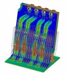
Deep Channel Analysis (continued)

                                  Tx Package
           Transmitter          Model, including           PCB Trace           Connector BOR            Connector
                                 PCB footprint

                                                                  Rx Package
                   Connector BOR             PCB Trace          Model, including            Receiver
                                                                 PCB footprint
                                          Tx                                          Rx

                                             Motherboard               Component Board

                               Components that typify a simple, standard 28 Gbps high-speed channel

     crosstalk and impedance must be considered. PCB                error levels well below manufacturing tolerance,
     design decisions include placement, routing, material/         which allows virtual prototyping. When combined
     laminate selection, trace lengths and impedance                with the speed and capacity of high-performance
     matching — all of which can enhance or adversely               computing (HPC), Samtec leverages HFSS accuracy
     affect the performance of the high-speed serial                to offer predictable correlation to measurements
     channel. The breakout region (BOR) of PCB traces               at frequencies up to 70 GHz. Driven by system
     from the connector is often overlooked, yet it can             inputs, Samtec can fine-tune channel variables,
     break a design.                                                like the connector BOR, via placement, trace type,
        Designing and optimizing the high-speed channel             manufacturing variability and other factors to drive
     requires two basic steps. Engineers must model each            accurate analysis and simulation across the channel.
     particular component in the channel. The channel               In addition, advances in HFSS solver technology
     model is created from the concatenation of these               for hybrid planar/3-D designs in HFSS 3-D Layout
     component models to form a complete system. The                have enabled Samtec engineers to rapidly prototype
     system model can then be simulated, modeled,                   complex interactions between components and PCBs,
     analyzed and tested at data rates of 28 Gbps and               compressing the time to solution from weeks to days,
     beyond.                                                        and from days to hours.

     Modeling Complex 3-D Components                                Optimizing IC Packages and PCBs
     Channel components, especially connectors and cable            Optimizing the signal channel requires optimizing
     assemblies, are complex 3-D mechanical structures              large integrated circuit (IC) packages and PCBs found
     that typically are mechanically modeled in industry-           within the channel. These components present
     standard MCAD tools. Samtec’s engineers port the               unique design challenges as well. Optimizing larger
     mechanical models into the ANSYS HFSS software tool            structures demands a wider view of the system
     to analyze and optimize 3-D structures with high-              and, in addition to
     frequency electromagnetic fields.                              high-frequency
        The flexibility of the state-of the-art 3-D full-wave       electromagnetic
     solvers in HFSS allows Samtec to target subcomponent           simulation and
     modeling as well. Modeling 3-D structures of                   analysis, engineers
     PCB traces, cables, RF launches and the complex                must consider power
     transitions between PCBs, the package and multichip            integrity, signal
     modules (MCMs) expand channel optimization                     integrity,
     capabilities.                                                  crosstalk and
        The accuracy of ANSYS HFSS also enables improved            EMI analysis of IC
     channel optimization. Solver accuracy can reach                packages and PCBs.

                       HFSS 3-D Components                                            MCAD 3-D rendering of Samtec MEC5-DV
                       ansys.com/HFSS-3D                                              connector and cable assembly

16   ANSYS ADVANTAGE                                                                                           ISSUE 3 | 2017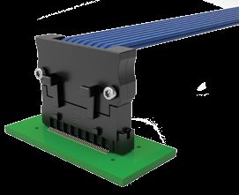
“The company continues to leverage the capability of ANSYS software
    to shorten product design cycles and expand its capabilities to provide
       next-generation products to tech industry performance leaders.                                      ”

    Samtec uses ANSYS SIwave                                                        ANSYS High-Performance
software to model and analyze                                                       Computing Options
large planar PCB and IC package                                                     Simulating, analyzing and
high-speed channels and complete                                                    optimizing the entire high-speed
power delivery networks (PDNs).                                                     channel signal path across
Using SIwave, Samtec can design                                                     multiple components can be time
current flow pathways, eliminate                                                    intensive. Samtec leverages the
current crowding and minimize                                                       HPC capabilities of the ANSYS
IR voltage drops virtually in                                                       tools to increase problem size and
internal connector test boards and                                                  complexity while minimizing
customer-specific applications.                                                     time-to-solution. Engineers can
Samtec can also model                  ANSYS HFSS-modeled electric field within     increase product performance while
                                       Samtec MEC5-DV connector and cable
resonances, reflections, inter-                                                     reducing the overall design cycle.
                                       assembly
trace coupling, simultaneous                                                            Samtec has developed the
switching noise, power/ground                                                       appropriate IT infrastructure to
bounce and DC voltage/current distributions, and               fully leverage the HPC features from the ANSYS tool
near- and far-field radiation patterns in connector            suite. Leveraging the HPC capabilities of ANSYS tools
breakout regions, packages and PCBs. Using what                is necessary to harness bigger, faster and higher-
Samtec terms “deep modeling technology,” SIwave                fidelity simulations. Like many companies, Samtec
models entire buses and packages using S-parameters            has engineering and signal-integrity resources located
with hundreds or thousands of ports in hours so                in many places with multicore servers and multiple
that Samtec designers and customers can identify               scalable computing clusters to fully unlock the HPC
critical signal integrity / power integrity issues             capabilities of the ANSYS tools across the world.
without guesswork. Problems that could not be                      For ANSYS HFSS and SIwave applications, Samtec
solved five years ago are now readily solved with              leverages highly parallelized clusters running HFSS
SIwave running in a high-performance computing                 to achieve full-wave solve times accelerated by
(HPC) environment.                                             10 times to 100 times. Engineers can perform large
                                                               connector modeling for customer system simulations
Circuit Simulations Across the Channel                         and extract large sections of packages with thousands
Once the channel has been modeled and characterized            of ports for deep analysis of potential issues.
electromagnetically with ANSYS HFSS and SIwave,
the remaining step is circuit simulation across the            Conclusion
channel. Samtec uses ANSYS Nexxim time-domain                  The combination of Samtec’s SI capabilities for 28 Gbps
circuit simulation engines to perform full-channel             (and faster) channels with ANSYS tools provides data-
simulations of a high-speed interconnect.                      center equipment OEMs a platform for deep channel
    Industry-standard IBIS-AMI drivers and receivers           analysis. Samtec is currently developing a 112 Gbps
act as signal transmitters and receivers across the            connectors, package and interconnect design, using
channel signal path. When used in combination with             ANSYS software to shorten product design cycles and
IBIS-AMI, the Nexxim circuit simulator represents              expand its capabilities to provide next-generation
the industry’s leading solution for high-speed                 products to tech industry performance leaders.
communication channel design. The ANSYS Nexxim
circuit solver combines IBIS-AMI models with the
                                                               Reference
channel performance model to provide SerDes circuit            [1] Cisco Visual Networking Index:
and timing analysis. This approach provides virtual                Global Mobile Data Traffic Forecast Update,
time-domain compliance to the Samtec design team.                  2016–2021 White Paper

© 2017 ANSYS, INC.                                                                                     ANSYS ADVANTAGE   17
You can also read