Drain Current Modeling of Tunnel FET using Simpson's Rule

 
CONTINUE READING
Drain Current Modeling of Tunnel FET using Simpson's Rule
Drain Current Modeling of Tunnel FET using
Simpson’s Rule
Arun A V (  arunav.aav@gmail.com )
 Model Engineering College https://orcid.org/0000-0002-8132-2233
Minu K K
 College of Engineering Poonjar
Sreelakshmi P S
 Model Engineering College
Jobymol Jacob
 College of Engineering Poonjar

Research Article

Keywords: Band to band tunneling, Drain current modeling, Simpson’s Rule, Tunnel Field Effect Transistor

Posted Date: July 1st, 2021

DOI: https://doi.org/10.21203/rs.3.rs-600894/v1

License:   This work is licensed under a Creative Commons Attribution 4.0 International License.
Read Full License
Drain Current Modeling of Tunnel FET using Simpson's Rule
Noname manuscript No.
(will be inserted by the editor)

Drain Current Modeling of Tunnel FET using Simpson’s Rule
Arun A V · Minu K K ·
Sreelakshmi P S · Jobymol
Jacob

Received: date / Accepted: date

Abstract Tunnel Field Effect Transistor can be introduced as an emerging alternate to MOSFET which is energy
efficient and can be used in low power applications. Due to the challenge involved in integration of band to
band tunneling generation rate, the existing drain current models are inaccurate. A compact analytical model for
simple tunnel FET and pnpn tunnel FET is proposed which is highly accurate. The numerical integration of tun-
neling generation rate in the tunneling region is performed using Simpson’s rule. Integration is done using both
Simpson’s 1/3 rule and 3/8 rule and the models are validated against numerical device simulations. The models
are compared with existing models and it is observed that the proposed models show excellent agreement with
device simulations in the entire region of operation with Simpson’s 3/8 rule exhibiting the maximum accuracy.
Keywords Band to band tunneling · Drain current modeling · Simpson’s Rule · Tunnel Field Effect Transistor

1 Introduction                                                tion, modulates the energy band profile, and shortens
                                                              the tunneling width [8].
Tunnel Field Effect Transistor (TFET) has been identi-            Several numerical models for TFET drain current
fied as a viable alternate to MOSFET in the nano scale        [9] [12] reported in literature are computationally com-
semiconductor device category [1] - [4]. Since the de-        plex and hence it is inefficient to do circuit simulations
vice operates on band to band tunneling (BTBT) [5] -          using these models. Investigations on various model-
[6] phenomena, it shows better resistance against short       ing approaches [13] - [17] point out the need to de-
channel effects observed in MOSFET. The major ad-             velop an accurate and computationally efficient ana-
vantage of TFET over MOSFET is that it provides a sub         lytical model for drain current of TFET. Integration of
threshold slope lesser than the minimum achievable            BTBT generation rate is a major challenge in drain cur-
limit of 60 mV/decade for MOSFET. Though the de-              rent modeling due to the presence of exponential and
vice is ambipolar in nature, the OFF current is compar-       polynomial terms. Tangent line approximation [18] -
atively low which makes it popular among memory               [19] is one of the preferred method for integration of
devices and the device is particularly suitable for low       BTBT generation rate. The tangent line approximation
power applications. Developing an accurate and com-           can be used to approximate functional values that de-
putationally efficient drain current model for TFET be-       viate slightly from exact values. Another method is to
comes important for performing fast and error free cir-       perform integration by approximating the function as
cuit simulations. The problem with the TFET device is         exponential and neglecting the polynomial term [15].
that it has low ON current. The band-to-band tunnel-              This paper reports a compact analytical drain cur-
ing rate has an exponential dependence [7] on the lat-        rent model for planar TFET which is accurate in the
eral electric field. Due to the low lateral electric field,   entire operating range. The model is extended to pnpn
the planar p-i-n TFET has low ON state current. TFET          TFET structure and it shows commendable accuracy.
with n+ pocket between source and channel is gener-           Here, the drain current model is formulated by numer-
ally known as pnpn TFET and exhibits significant im-          ical integration of BTBT generation rate using Simp-
provement in ON state current. This is because the n+         son’s rule. Both 1/3 and 3/8 rule is employed for model
pocket increases the electric field in the lateral direc-     derivation and the models are compared for its accu-
2

                                                                                                   0.8

                                                                                                   0.6

                                                                                                   0.4

                                                                           Surface Potential (V)
                                                                                                   0.2

                                                                                                                   R0        R1               R2               R3
                                                                                                   0.0

                                                                                                   -0.2

                                                                                                   -0.4

                                                                                                   -0.6

                                                                                                   -0.8

                                                                                                   -1.0

                                                                                                   -1.2       x0        x1        x2                      x3        x4
Fig. 1 Schematic view of p-channel SOI TFET
                                                                                                          0        50         100       150        200     250           300

                                                                                                                        Distance Along the Channel (nm)

racy. BTBT generation rate is a function of electric field     Fig. 2 Plot of surface potential vs distance along the channel
which is derived from surface potential. The model is          showing the classification of regions of the p-channel TFET for
                                                               VGS = −1V and VDS = −0.5V [17]
validated against 2D numerical device simulation us-
ing Silvaco Atlas [20]. The device simulation tool is
calibrated against published experimental data [16] -          constant in this region, the electric field in this region
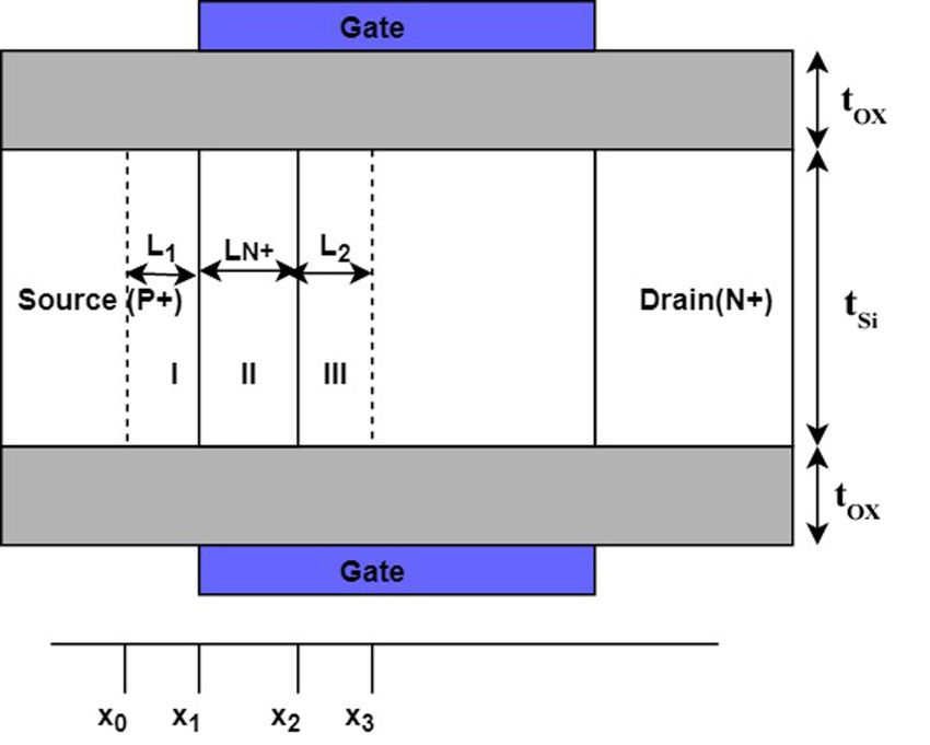
[17] [21] - [28]. A Cross section of p-channel SOI TFET        becomes negligible.
used for simulation and validation is shown in Fig. 1.             2D Poisson equation for the surface potential of TFET [17]
    The drain current model published in literature [17],      is given by
due to its tangent line approximation of the parabolic
                                                                δ2            δ2           qNA
function has limited accuracy. Simpson’s rule approxi-            2
                                                                    (x, y) +    2
                                                                                  (x, y) =                                                                                           (1)
                                                               δx            δy             ǫSi
mates BTBT generation rate function as parabolic seg-
ments. Hence, the proposed method of drain current             Applying parabolic approximation [26] of potential in
formulation demonstrates excellent match with the de-          y direction and substituting y=0 in equation (1) to ob-
vice simulations.                                              tain surface potential as
    The paper is organized in the following manner.
                                                                                                                                                                                qNA L2dj
                                                                                                                                                            
Section II discusses model development followed by                                                                  x                                    −x
                                                               ψsj (x) = Cj exp                                                   + D exp                            + ψ(G) −
model validation in section III. Section IV concludes                                                              Ldj                                   Ldj                      ǫSi
the work.                                                                                                                                                                          (2)
                                                               where Ldj is the characteristic length and in region R1 ,
                                                               it is given by
2 Model Development
                                                                       r
                                                                         tSi tox ǫSi
The investigation is performed on a planar p-channel           Ld1 =                                                (3)
                                                                             ǫox
SOI TFET having with channel length (L) = 200 nm,
                                                               The gate potential ψ(G) can be expressed as
length of source region (LS )=50 nm, length of drain
region (LDr )=50 nm, body doping (NA ) = 1015 /cm3 ,            (G) = VGS − VFB                                                                                                      (4)
source (NS ) = 1020 /cm3 , drain doping (NDr ) = 1019 /cm3 ,
                                                               where VFB is the flat band voltage.
thickness of oxide layer(tox ) = 2 nm, thickness of sili-
                                                               Applying boundary conditions, the final solution for
con film (tSi ) = 10 nm, and work function of gate-metal
                                                               the surface potential in R1 [17] is
is φ = 4.8 eV [13].
    Drain current is formulated by the integration of
generation rate over the entire volume. An accurate
                                                                                                                                                                                
                                                                                                                                        x−(Ld1 cosh−1 (Vbi /(ψC −ψG )
                                                               ψs1 (x) = (ψC − ψG )cosh−1                                                           Ld1                              + ψG
surface potential model and an error free integration
method result in drain current model with high level                                                                                                                                 (5)
of accuracy.                                                   and in R2
                                                               ψs3 (x) = ψC                                                                                                          (6)
2.1 Surface Potential and Electric Field                       The electric field is given by

The surface potential of p-channel TFET with respect                     δψsj (x)
                                                               E(x) = −                                              (7)
to distance along the channel is plotted in Fig. 2. From                    δx
the plot it is observed that in region R2 the potential is     This field is applied to the tunneling generation rate to
almost constant and is represented as ψC . Since ψC is         find the drain current.
3

2.2 Surface Potential in Source Body and Drain body               ∂ψsj                   ∂ψsj−1
                                                                        (at x = xj−1 ) =        (at x = xj−1 )        (18)
Depletion Regions                                                   ∂x                     ∂x
                                                                  Substituting equation (10) into equation (17) and equa-
The parabolic approximation adopted in region R1 is               tion (18)
valid for depletion regions. Considering the gate fring-
                                                                                          L
ing field, boundary conditions relating to continuity                            Ldj+1 − L j
                                                                  2Dj+1 = (1 −        )e dj Cj
of electric field varies in the depletion region. This is                         Ldj
                                                                                                                       (19)
due to the modified gate body capacitance generally                               Ldj+1 L j
                                                                                           L

known as fringing capacitance. The gate body capaci-                       + (1 +      )e dj Dj + (ψCj − ψCj+1 )
                                                                                   Ldj
tance is modified by applying conformal mapping tech-
niques [29], and is shown in equation(8)
                                                                                          L
                                                                                 Ldj+1 − L j
        2                                                         2Cj+1 = (1 −        )e dj Cj
Coxf   = Cox                                             (8)                      Ldj
        π                                                                                                              (20)
                                                                                          L
                                                                                  Ldj+1 L j
So the boundary condition changes as                                       + (1 +      )e dj Dj + (ψCj − ψCj+1 )
                                                                                   Ldj
∂ψ              −Coxf (ψG − ψs0 )
   (at y = 0) =                                          (9)      By applying diode approximation, the depletion re-
∂y                     ǫSi
                                                                  gion lengths are given by
Applying this boundary condition in Region R0                          s
                                                                         2ǫSi |ψC2 − VS |N2
                                                                  L1 =                                          (21)
                x − xi                x − xi          2qN0 L2d0           q|N1 |(|N1 + N2 |)
ψs0 = C0 exp(          ) + D0 exp − (        ) + ψG −
                 Ld0                   Ld0              ǫSi            s
                                                        (10)             2ǫSi |VDS − ψC2 |N2
                                                                  L3 =                                          (22)
                                                                           q|N4 |(|N4 + N2 |)
where
      r                                                           C0 , C2 , D0 and D2 are obtained by solving equations
        πtSi tox ǫSi                                              (19) and (20).
Ld0 =                                                   (11)
           2ǫox
and
                                                                  2.3 BTBT Generation Rate
       2qNj L2dj
ψG −               = ψCj                                (12)      Kane’s band to band tunneling model [30] is derived
          ǫSi
                                                                  with constant electric field applied to time indepen-
where Nj is the doping in jth region. Similar equations           dent Schrodinger equation. In this model, the basis func-
can be written in drain body depletion region.                    tion was represented using Bloch function. For evalu-
   In the source body depletion region, the boundary              ating transmission probability, Kane applied perturba-
conditions in x direction are                                     tion theory. Though the derivation involved in Kane’s
ψs0 (xi ) = VS + Vbi0                                   (13)      model is complex, an expression for tunneling per cu-
                                                                  bic centimeter can be derived which is given by.
∂ψs0
      (at x = xi ) = 0                            (14)                                    "     3/2
                                                                                                         #
  ∂x                                                                        E2 m∗1/2        −πEg m∗1/2
                                                                  GBT B =         1/2
                                                                                      exp                             (23)
where Vbi0 is the built-in voltage of the source body                      18πh2 Eg             2hE
region. Similarly, boundary conditions in x direction
at drain body depletion region are                                where E is the uniform electric field, m∗ is the effective
                                                                  mass of the carrier and Eg represents the band gap en-
ψs3 (x2 ) = VDS + Vbi2                                  (15)      ergy. Equation (23) can be reduced to
∂ψs2
                                                                                       
      (at x = x2 ) = 0                              (16)                      2      −B
  ∂x                                                              GBT B = AE exp                                        (24)
                                                                                      E
where Vbi2 is the built-in voltage of the drain body
                                                                  Keldysh et.al [31] modified equation (24) to
region. At the source body and drain body interface,
applying boundary continuity of surface potential and
                                                                                         
                                                                                       −B
electric field displacement the surface potential is ob-          GBT B = AE2.5 exp                                    (25)
                                                                                        E
tained as
                                                                  In both cases, the parameters A and B are linear and
ψsj (xj−1 ) = ψsj−1 (xj−1 )                             (17)      exponential parameters respectively.
4

                                                                                                                 in Fig.3. The three points are x0 , x00 and the mid point
                                                    38
                                             7x10
                                                                                                                 of x0 and x00 . x00 is the point where BTBT tunneling
                                                    38
                  s)

                                             6x10
                                                                                                                 generation rate approaches zero.
                  3
                  BTBT Generation Rate(/cm

                                                    38
                                             5x10

                                                    38
                                             4x10

                                             3x10
                                                    38

                                                                                                                 GBT B (x0 ) = a0 + a1 x0 + a2 x20                                                                                  (29)
                                                    38
                                             2x10

                                                    38
                                             1x10

                                                                                                                               x0 + x00              x + x00         x + x00 2
                                                    0
                                                                                                                 GBT B (                ) = a0 + a1 ( 0      ) + a2 ( 0     )
                                                         x0   50.0     50.5    51.0     51.5       52.0   52.5                    2                     2               2
                                                                     Distance along channel (nm)           x00
                                                                                                                                                                                                                                    (30)
Fig. 3 Plot of BTBT generation rate along the channel
                                                                                                                 GBT B (x00 ) = a0 + a1 x00 + a2 x200                                                                               (31)

2.4 Drain Current Model using Simpson’s Rule                                                                     solving above three equations yields
                                                                                                                                                                                          x +x00
                                                                                                                        x20 GBT B (x00 )+x0 x00 GBT B (x00 )−4x0 x00 GBT B ( 0 2                   )+x0 x00 GBT B (x0 )+x200 GBT B (x0 )
The band to band tunneling generation rate in source                                                             a0 =                                          x20 −2x0 x00 +x200
body depletion region is given by equation (25) and                                                                                                                                                                                 (32)
is plotted in Fig 3. The expression contains polyno-
mial as well as exponential terms which limits direct
                                                                                                                                                       x0 +x00                                                      x0 +x00
integration. Extensive modeling approximation can be                                                             a1 = −
                                                                                                                          x0 GBT B (x0 )−4x0 GBT B (       2     )+3x0 GBT B (x00 )+3x00 GBT B (x0 )−4x00 GBT B (       2     )+x00 GBT B (x00 )
                                                                                                                                                                            x20 −2x0 x00 +x200
adopted in such cases, by eliminating the polynomial                                                                                                                                                                                (33)
term, if the accuracy is not compromised. Here, if such
approximations are made, the drain current model be-                                                                         GBT B (x0 ) − 2GBT B ( x0 +x 00
                                                                                                                                                             )GBT B (x00 )
                                                                                                                                                       2
comes highly inaccurate. So band to band tunneling                                                               a2 = 2                   2                2
                                                                                                                                                                                                                                    (34)
                                                                                                                                         x0 − 2x0 x00 + x00
generation rate is numerically integrated over the en-
tire tunneling volume to obtain the drain current. The                                                               Substituting the coefficients a0 , a1 and a2 from equa-
numerical method used here is Simpson’s rule which                                                               tions (32) to (34) in equation (28) and multiplying the
is an extension of trapezoidal rule. Numerical integra-                                                          integral by electronic charge, q yields the drain current
tion is performed using both Simpson’s 1/3 rule and                                                              in equation (26) as
3/8 rule.

                                                                                                                                  ltunnel h                       x0 + x00                 i
                                                                                                                 ID = qZ                   GBT B (x0 ) + 4GBT B (          ) + GBT B (x00 )
2.5 Model using Simpson’s 1/3 rule                                                                                                   6                               2
                                                                                                                                                                                (35)
In this approach, the integrand is obtained by approx-
imating it as second order polynomial. The drain cur-                                                            Here x0 and x00 are boundaries of tunneling region
rent is given as                                                                                                 [17].
        Z
ID = q GBT B (x)dx                                (26)                                                           x 0 = LS − L1                                                                                                      (36)

The tunneling region along the channel is defined from
x0 to x00 as shown in Fig. 3. The GBT B function is ap- x00 = LS + Ld1 cosh−1 ((ψs1 − ψG − Eg /q) − (ψC − ψG ))
proximated to a second order polynomial and integrated                                                     (37)
over the tunneling region yields
Z x00               Z x00                               ltunnel = x00 − x0                                 (38)
                                           2
      GBT B (x)dx =       (a0 + a1 x + a2 x )dx    (27) Z is given by
 x   0               x                                        0

                                                                                                                          Atinversion
Z x00                                                                                                            Z=
                                          x2 − x20     x3 − x30
                                                                                                                             p
                                                                                                                               Eg
         GBT B (x)dx = a0 (x00 − x0 ) + a1 00      + a2 00
    x0                                        2            3
                                                                                                                 where tinversion is the inversion layer thickness A
                                                           (28)
                                                                                                                 is the BTBT parameter given by (25). This analytical
To evaluate the polynomial coefficients a0 , a1 and a2 ,                                                         model provides a closed form equation for drain cur-
choose three points in the x axis of the graph shown                                                             rent which is suitable for circuit simulations.
5

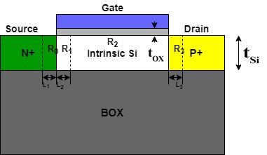
                                                                 2.6 Drain Current Model for pnpn TFET

                                                                 In comparison with the p-i-n TFET, the pnpn TFET
                                                                 structure is more promising for low-power circuit de-
                                                                 sign [32]. Fig. 4 shows the cross section of the device
                                                                 considered in the analysis with gate length (LG ) = 60
                                                                 nm, body doping (N3 = N4 ) = 1015 /cm3 , source and
                                                                 drain doping (NS and NDr ) = 1020 /cm3 , length of source/drain
                                                                 regions (LS /LD r) = 70 nm, pocket length (LN+ ) = 6nm,
                                                                 pocket doping(N+)=2X10¹⁹ /cm3 , thickness of oxide layer
                                                                 (tox ) = 2 nm, thickness silicon film (tSi ) = 10 nm, and
Fig. 4 Schematic of the double-gate pnpn TFET structure          work function of gate-metal φ = 4.33 eV [33].
                                                                     Using parabolic approximation the surface poten-
                                                                 tial of the device[26] is found out to be
2.5.1 Model using Simpson’s 3/8 Rule
                                                                 ψSj (x) = Cj eu(x−xj−2 ) + Dj e−u(x−xj−2 ) + ψdj   (47)
Simpson’s 3/8 rule for integration is derived by ap-
                                                                 where 1/u is the characteristic length and j = 2-4 is
proximating the given function with the third order
                                                                 applicable for regions II − IV respectively.
(cubic) polynomial.
                                                                    In region I the potential is given by

GBT B (x) = a0 + a1 x + a2 x2 + a3 x3                     (39)               qNeff
                                                                 ψs1 (x) =         (x + L1 )2 − ψsrc                (48)
                                                                              2ǫSi
To evaluate the polynomial coefficients a0 , a1 , a2 and a3 , where
choose four points in the x axis of the graph shown in
                                                                            2Cf
Fig.3. The four points are x0 , x01 , x02 , x00 . Where x01   Neff = Nsrc −       (VGS − VFB − ψsrc )               (49)
and x02 are given by                                                        qt Si

                                                                             kT NS
            l                                                    ψsrc = −      ln                                   (50)
x01   = x0 + tunnel                                       (40)               q    ni
               3
                                                                 Expression for x0 remains the same as in equation (36)
                                                                 and the value of xk [26] changes to
             2ltunnel
x02 = x0 +                                                (41)               1
                 3                                               xk = LS +      cosh−1 ((ψs2 − ψG − Eg /q) − (ψC − ψG ))
                                                                             u3
GBT B (x0 ) = a0 + a1 x0 + a2 x20 + a3 x30                (42)                                                      (51)

                                                                 Electric field is obtained as the derivative of surface
GBT B (x01 ) =   a0 + a1 x01 + a2 x201   + a3 x301        (43)   potential and is applied in generation rate. Drain cur-
                                                                 rent is modeled using Simpson’s 1/3 and 3/8 rule by
GBT B (x02 ) = a0 + a1 x02 + a2 x202 + a3 x302            (44)   applying generation rate in equation (35) and (46) re-
                                                                 spectively.

GBT B (x00 ) = a0 + a1 x00 + a2 x200 + a3 x300            (45)
                                                               3 Model Validation
Solving for a0 , a1 , a2 and a3 and substituting in GBT B (x),
the drain current computed with Simpson’s 3/8 rule is          Even after the availability of an accurate surface poten-
obtained as                                                    tial model, it is difficult to obtain a drain current model
                                                               by direct integration due to the reason specified in sec-
         ltunnel                                               tion II. In this paper, a novel method of drain current
ID = qZ            [GBT B (x0 ) + 3GBT B (x01 )
            8                                         (46)     formulation using a numerical integration method called
                    + 3GBT B (x02 ) + GBT B (x00 )]            Simpson’s 1/3 rule and Simpson’s 3/8 rule is proposed.
                                                               To evaluate the suitability of the model, the proposed
This analytical model provides a closed form equation          drain current model is compared with the device sim-
for drain current.                                             ulations. While performing the device simulations, the
6

                         5.00E-008

                                                                                                                                                          -7
                                                                                                                                                1.0x10
                     0.00E+000

                                                                                                                                                          -8
                     -5.00E-008                                                                                                                 8.0x10                                             Simulation

                                                                                                                                                                                                   Proposed Model(1/3)
         ID(A/ mm)

                                                                                                                                                                                                   Proposed Model(3/8)
                     -1.00E-007                                                    Simulation

                                                                                                                                   |ID|(A/ m)
                                                                                                                                                          -8
                                                                                                                                                6.0x10                                             Tangent Line
                                                                                   Proposed Model(1/3)

                                                                                                                                  m
                                                                                                                                                                                                   exponential approximation
                     -1.50E-007                                                    Tangent Line

                                                                                   exponential approximtion
                                                                                                                                                          -8
                                                                                                                                                4.0x10
                                                                                   Proposed Model(3/8)
                     -2.00E-007

                                                                                                                                                          -8
                     -2.50E-007                                                                                                                 2.0x10

                     -3.00E-007
                                                                                                                                                     0.0

                     -3.50E-007
                                                  -3.0     -2.5     -2.0         -1.5        -1.0      -0.5         0.0                                    -3.0       -2.5            -2.0          -1.5             -1.0          -0.5   0.0

                                                                             V      (V)                                                                                                         VGS (V)
                                                                               GS

Fig. 5 Comparison of ID vs VGS given by the proposed model,                                                               Fig. 8 Comparison of ID vs VGS given by the proposed model,
existing model [17] and device simulation for P channel TFET                                                              existing model [17] and device simulation for P channel TFET
with VDS = −0.05V                                                                                                         with VDS = −0.05V with 20nm channel length

                                                                                                                                                          0
                                        0.0

                                                                                                                                                          -7                     19        -3
                                                                                                                                                  -1x10           Nsrc =Ndr=10        cm
                                         -7
                         -2.0x10

                                                                                                                                       ID(A/ m)
              ID(A/ m)

                                                                                                                                                          -7
                                                                                                                                                  -2x10

                                                                                                                                   m
           m

                                                                                                                                                                                                         Simulation
                                         -7                                 Simulation
                         -4.0x10                                                                                                                                                                         Proposed Model(1/3)
                                                                            Proposed Model(1/3)                                                           -7                                             Proposed Model(3/8)
                                                                                                                                                  -3x10
                                                                            Proposed Model(3/8)
                                                                                                                                                                                                         Tangent Line
                                                                            Tangent Line
                                                                                                                                                                                                         exponential approximation
                                         -7                                 exponential approximation
                         -6.0x10                                                                                                                          -7                                                            18        -3
                                                                                                                                                  -4x10                                                Nsrc =Ndr=10          cm

                                                                                                                                                          -7
                                         -7                                                                                                       -5x10
                         -8.0x10
                                                                                                                                                           -3.0       -2.5            -2.0          -1.5             -1.0          -0.5   0.0
                                             -3.0        -2.5     -2.0      -1.5          -1.0      -0.5      0.0

                                                                                                                                                                                                   VGS(V)
                                                                           VGS (V)

Fig. 6 Comparison of ID vs VGS given by the proposed model,                                                               Fig. 9 Comparison of ID vs VGS given by the proposed model,
existing model [17] and device simulation for P channel TFET                                                              existing model [17] and device simulation for P channel TFET
with VDS = −2V                                                                                                            with VDS = −0.05V for different source and drain doping

                                             -7                                                                                                           -4
                                      2x10                                                                                                      1.6x10

                                             -7                                                                                                           -4
                                      2x10                                                                                                      1.4x10

                                             -7
                                                                                                                                                                                                   Simulation
                                      2x10                                                                                                                -4
                                                                                                                                                1.2x10                                             Proposed Model(3/8)

                                                                                                                                                                                                   Proposed Model(1/3)
                                             -7
                                      2x10
                                                                                                                                                          -4                                       Tangent Line
                                                                                                                                                1.0x10
                                                                                                                                                                                                   exponential approximation
                         |ID|(A/ m)

                                                                                                                                  ID(A/ mm)

                                             -7             Simulation
                                      1x10
                     m

                                                            Proposed Model(1/3)                                                                           -5
                                                                                                                                                8.0x10
                                             -7
                                      1x10                  Proposed Model(3/8)

                                                            Tangent Line
                                                                                                                                                          -5
                                             -7                                                                                                 6.0x10
                                      1x10                  exponential approximation

                                             -7                                                                                                           -5
                                      1x10                                                                                                      4.0x10

                                             -7
                                      1x10                                                                                                                -5
                                                                                                                                                2.0x10

                                             -8
                                      9x10
                                                                                                                                                     0.0
                                                                                                                                                           0.0          0.2                  0.4               0.6            0.8         1.0
                                              -3.0       -2.5     -2.0       -1.5         -1.0      -0.5      0.0

                                                                                                                                                                                                   V     (V)
                                                                                                                                                                                                    GS
                                                                           VDS (V)

Fig. 7 Comparison of ID vs VDS curve given by the proposed                                                                Fig. 10 Comparison of |ID | vs VGS given by the proposed
model, existing model [17] and device simulation for P channel                                                            model, existing models and device simulation for VDS = 1V
TFET with VGS = −2V                                                                                                       for pnpn TFET

models used are concentration dependent mobility, elec-                                                                   tion [17] and by neglecting the polynomial term in the
tric field dependent mobility, Shockley-Read-Hall re-                                                                     band to band tunneling generation rate [15].
combination, Auger recombination, bandgap narrow-                                                                             Fig. 5 and Fig. 6 shows the validation of models
ing and Kane’s band-to-band tunneling. The constants                                                                      with device simulation when VDS is −0.05V and −2V
in Kane’s band-to-band tunneling model is fixed as                                                                        respectively. The proposed models show excellent agree-
AKane = 4X10¹⁹ and BKane = 41 [20] so that they re-                                                                       ment with the device simulations for the entire range
semble experimental results [25]. The proposed mod-                                                                       of VGS . Model With Simpson’s 3/8 rule (equation (44))
els are also compared with the existing drain current                                                                     is slightly more accurate than that with Simpson’s 1/3
models derived by applying tangent line approxima-                                                                        rule (equation 35). However, the computational time
7

                                                                                     actual device behavior in saturation region as shown
                       1E-5

                       1E-6
                                                                                     in Fig. 7. The model is also validated with different
                       1E-7

                       1E-8
                                                                                     source and drain dopings as shown in Fig. 9. The pro-
                       1E-9                                                          posed model is accurate with different doping concen-
                      1E-10
         ID(A/ mm))

                      1E-11                 Simulation                               trations.
                                            Propsed Model(3/8)
                      1E-12

                      1E-13
                                            Proposed Model(1/3)

                                            Tangent Line
                                                                                         The proposed drain current models for pnpn TFET
                      1E-14
                                            exponential approximation
                                                                                     is validated against numerical device simulations. So
                      1E-15

                      1E-16                                                          far, no published models are there for the drain current
                      1E-17

                      1E-18
                                                                                     of pnpn TFET. Fig. 10 and Fig. 11 shows the ID vs VGS
                              0.0   0.2   0.4

                                                V   (V)
                                                          0.6     0.8   1.0
                                                                                     plot for VDS = 1 V and VDS = 0.2 V respectively. The
                                                GS

                                                                                     plots show excellent match between the models and
Fig. 11 Comparison of ID vs VGS in log scale given by the pro-                       simulation results for different device parameters.
posed model, existing models and device simulation for VDS =
0.2V for pnpn TFET

                                                                                     4 Conclusion
associated with Simpson’s 3/8 rule, because of its third
order polynomial approximation is significantly higher                               In this paper, a compact analytical models for the drain
than the one associated with Simpson’s 1/3 rule which                                current of a planar TFET and pnpn TFET are reported.
uses only second order polynomial approximation. Fig.                                Investigations on the drain current modeling approaches
7 shows the output characteristics (ID –VDS ) for VGS =                              indicate the need for an accurate method for integra-
−2V. The proposed models has a slight error in the sat-                              tion of tunneling generation rate in the source body
uration region. This is due to the inaccuracy of surface                             junction. The proposed modeling approach is based on
potential model at high drain voltages.                                              integration of the tunneling generation rate by Simp-
    A short-channel TFET with channel length of 20                                   son’s rule. Both 1/3 and 3/8 rule are used for numer-
nm is also used in th analysis and compared with the                                 ical integration of tunnelling generation rate function.
models in Fig. 8. The proposed models are in good                                    The band to band tunneling generation function is ap-
agreement with the simulation results and hence the                                  proximated by sequence of quadratic parabolic seg-
model is suitable upto a channel length of 20 nm.                                    ments in both the proposed models, whereas in the
    In the existing method [17], drain current is calcu-                             existing model with tangent line approximation, it is
lated by integration of generation rate using tangent                                done by straight line segments. While developing the
line approximation. Integration is done by dividing the                              model the source side depletion region is also taken
tunneling generation rate shown in Fig. 3 into linear                                into account. The results demonstrate excellent agree-
segments and calculating the area under the graph us-                                ment of the model with device simulations. The accu-
ing triangular approximation. On the other hand, Simp-                               racy is proved in both ON state and subthreshold re-
son’s rule approximates the graph with sequence of                                   gion for different device dimensions.
quadratic parabolic segments instead of straight lines.
This makes the model more accurate which closely por-
trays the device behavior in the entire operating range.                             Declarations
    In the existing model, the tangent line is drawn to
the generation rate function y = Gbtb (x) at a particular                            Funding Statement
point x = a and the value of y is then linearly approx-
imated. Now the linear approximation to Gbtb (x) is                                  The authors would like to acknowledge the Depart-
written as                                                                           ment of Science and Technology (DST), Government of
                                                                                     India for providing improved Science and Technology
                   ′                                                                 infrastructure for research work, through FIST project.
L(x) = Gbtb (a) + Gbtb (a)(x − a)                                             (52)
                                                                                     The authors would also like to thank Centre for En-
If the possible error in x is xe , the possible error in y is                        gineering Research and Development (CERD) for the
given by                                                                             seed money project fund to initiate this research work.
          
          dy
ye = xe                                                  (53)
          dx x=a
                                                                                     Conflict of Interest
Here xe depicts the error in surface potential and ye is
the total error in drain current. This demonstrates the                              The authors declare that they have no conflict of inter-
mismatch of the existing drain current model with the                                est
8

Author Contributions                                            References

    1 Arun A V: Conceptualization, formal analysis, in-  1. Datta S, Liu H, Narayanan V. Tunnel FET technol-
                                                            ogy: A reliability perspective. Microelectronics Reliability
      vestigation methodology, device simulation, math-     2014;54(5):861–874. doi.org/10.1016/j.microrel.2014.02.002
      ematical modeling, validation, writing- original draft.
                                                         2. Wang H, Chang S, Hu Y, He H, He J, Huang Q, et al. A
    2 Minu K K: Mathematical Analysis, modeling method-     novel barrier controlled tunnel FET. IEEE electron device let-
      ology, writing - review and editing.                  ters 2014;35(7):798–800. doi.org/10.1109/LED.2014.2325058
                                                         3. Asra R, Shrivastava M, Murali KV, Pandey RK, Goss-
    3 Sreelekshmi P S: Formal analysis, device simula-      ner H, Rao VR. A tunnel FET for VDD scaling be-
      tion, validation                                      low 0.6 V with a CMOS-comparable performance. IEEE
    4 Jobymol Jacob: Conceptualization, formal analy-       Transactions on Electron Devices 2011;58(7):1855–1863.
      sis, investigation methodology, device simulation,    doi.org/10.1109/TED.2011.2140322
                                                         4. Ionescu AM, Riel H. Tunnel field-effect transistors as energy-
      mathematical modeling, validation, writing- review    efficient electronic switches. nature 2011;479(7373):329–337.
      and editing, supervision.                             doi.org/10.1038/nature10679
                                                         5. Schenk A, et al. Rigorous theory and simplified model of
                                                            the band-to-band tunneling in silicon. Solid-State Electronics
                                                            1993;36(1):19–34. doi.org/10.1016/0038-1101(93)90065-X
Availability of data and material                        6. You KF, Wu CY. A new quasi-2-D model for hot-carrier band-
                                                            to-band tunneling current. IEEE Transactions on Electron De-
                                                            vices 1999;46(6):1174–1179. doi.org/10.1109/16.766880
Not applicable                                           7. Shen C, Yang LT, Samudra G, Yeo YC. A new robust
                                                            non-local algorithm for band-to-band tunneling simulation
                                                            and its application to Tunnel-FET. Solid-State Electronics
                                                            2011;57(1):23–30. doi.org/10.1016/j.sse.2010.10.005
Compliance with ethical standards                        8. Abdi, Dawit Burusie, and Mamidala Jagadesh Kumar.
                                                            ”In-built N+ pocket pnpn tunnel field-effect transistor.”
                                                            IEEE Electron Device Letters 35.12 (2014): 1170-1172.
Not applicable                                              https://doi.org/10.1109/LED.2014.2362926
                                                         9. Cui N, Liang R, Wang J, Xu J. Si-based hetero-material-
                                                            gate tunnel field effect transistor: Analytical model and
                                                            simulation. In: 2012 12th IEEE International Conference
Consent to participate                                      on Nanotechnology (IEEE-NANO) IEEE; 2012. p. 1–5.
                                                            doi.org/10.1109/NANO.2012.6321906
Not applicable                                           10. Cui N, Liang R, Wang J, Xu J. Two-dimensional ana-
                                                            lytical model of hetero strained Ge/strained Si TFET.
                                                            In: 2012 International Silicon-Germanium Technol-
                                                            ogy and Device Meeting (ISTDM) IEEE; 2012. p. 1–2.
                                                            doi.org/10.1109/ISTDM.2012.6222412
Consent for publication                                  11. Lee MJ, Choi WY. Analytical model of single-gate
                                                            silicon-on-insulator (SOI) tunneling field-effect transis-
Not applicable                                              tors (TFETs). Solid-State Electronics 2011;63(1):110–114.
                                                            doi.org/10.1016/j.sse.2011.05.008
                                                         12. Liu L, Mohata D, Datta S. Scaling length theory of
                                                            double-gate interband tunnel field-effect transistors. IEEE
                                                            Transactions on Electron Devices 2012;59(4):902–908.
Acknowledgment                                              doi.org/10.1109/TED.2012.2183875
                                                         13. Mohammadi, Saeed, and Danial Keighobadi. ”A universal
This work was supported in part by Department of            analytical potential model for double-gate Heterostructure
Science and Technology (DST), Government of India           tunnel FETs.” IEEE Transactions on Electron Devices 66.3
                                                            (2019): 1605-1612. doi.org/10.1109/TED.2019.2895277
through FIST project under Dy. No: 100/IFD/4185/2013- 14. Keighobadi, D., and S. Mohammadi. ”Physical and analyti-
14 and Centre for Engineering Research and Devel-           cal modeling of drain current of double-gate heterostructure
opment (CERD) through seed money project.The ac-            tunnel FETs.” Semiconductor Science and Technology 34.1
knowledgement is extended to Microelectronics and           (2018): 015009. doi.org/10.1088/1361-6641/aaeeeb
                                                         15. Mohammadi, Saeed, and Hamid Reza Tajik Khaveh. ”An
MEMS Laboratory, Electrical Engineering Department,         analytical model for double-gate tunnel FETs considering the
IIT Madras for providing us with the facility to use the    junctions depletion regions and the channel mobile charge
device simulation tools.                                    carriers.” IEEE Transactions on Electron Devices 64.3 (2017):
                                                            1276-1284. doi.org/10.1109/TED.2017.2655102
                                                         16. Verhulst AS, Sorée B, Leonelli D, Vandenberghe WG, Groe-
                                                            seneken G. Modeling the single-gate, double-gate, and gate-
                                                            all-around tunnel field-effect transistor. Journal of Applied
Correspondence Author                                       Physics 2010;107(2):024518. doi.org/10.1063/1.3277044
                                                         17. Vishnoi R, Kumar MJ. An accurate compact analytical
Correspondence to Arun A V, email:arunav.aav@gmail.com model for the drain current of a TFET from subthreshold
9

   to strong inversion. IEEE Transactions on Electron Devices
   2015;62(2):478–484. doi.org/10.1109/TED.2014.2381560
18. Mahfouf JF. Influence of physical processes on the
   tangent-linear     approximation.     Tellus   A:     Dynamic
   Meteorology and Oceanography 1999;51(2):147–166.
   doi.org/10.3402/tellusa.v51i2.12312
19. Park SK, Droegemeier KK. Validity of the tangent
   linear approximation in a moist convective cloud
   model. Monthly weather review 1997;125(12):3320–3340.
   doi.org/10.1175/1520-0493(1997)125
20. Int S, Santa Clara C, et al. ATLAS device simulation soft-
   ware. Santa Clara, CA, USA 2014;.
21. Bhushan B, Nayak K, Rao VR. DC compact model
   for SOI tunnel field-effect transistors. IEEE trans-
   actions on electron devices 2012;59(10):2635–2642.
   doi.org/10.1109/TED.2012.2209180
22. Kane E. Zener tunneling in semiconductors. Journal
   of Physics and Chemistry of Solids 1960;12(2):181–188.
   doi.org/10.1016/0022-3697(60)90035-4
23. Young KK. Short-channel effect in fully depleted
   SOI MOSFETs. IEEE Transactions on Electron Devices
   1989;36(2):399–402. doi.org/10.1109/16.19942
24. Kumar MJ, Chaudhry A. Two-dimensional analytical mod-
   eling of fully depleted DMG SOI MOSFET and evidence
   for diminished SCEs. IEEE Transactions on Electron Devices
   2004;51(4):569–574. doi.org/10.1109/TED.2004.823803
25. Vishnoi R, Kumar MJ. Compact analytical model of
   dual material gate tunneling field-effect transistor us-
   ing interband tunneling and channel transport. IEEE
   Transactions on Electron Devices 2014;61(6):1936–1942.
   doi.org/10.1109/TED.2014.2315294
26. Wan J, Le Royer C, Zaslavsky A, Cristoloveanu S. A tun-
   neling field effect transistor model combining interband tun-
   neling with channel transport. Journal of Applied Physics
   2011;110(10):104503. doi.org/10.1063/1.3658871
27. Vandenberghe W, Verhulst AS, Groeseneken G, Soree
   B, Magnus W. Analytical model for point and line
   tunneling in a tunnel field-effect transistor. In: 2008
   International Conference on Simulation of Semicon-
   ductor Processes and Devices IEEE; 2008. p. 137–140.
   doi.org/10.1109/SISPAD.2008.4648256
28. Verhulst AS, Leonelli D, Rooyackers R, Groeseneken
   G. Drain voltage dependent analytical model of tun-
   nel field-effect transistors. Journal of Applied Physics
   2011;110(2):024510. doi.org/10.1063/1.3609064
29. Zhang,      Lining,    et    al.  ”An     analytical   charge
   model for double-gate tunnel FETs.” IEEE Trans-
   actions on Electron Devices 59.12 (2012): 3217-
   3223.doi.org/10.1109/TED.2012.2217145
30. Kane EO. Theory of tunneling. Journal of applied Physics
   1961;32(1):83–91. doi.org/10.1063/1.1735965
31. Zheltikov A. Keldysh parameter, photoionization adi-
   abaticity, and the tunneling time. Physical Review A
   2016;94(4):043412. doi.org/10.1103/PhysRevA.94.043412
32. Ram, Mamidala Saketh, and Dawit Burusie Abdi. ”Doping-
   less PNPN tunnel FET with improved performance: design
   and analysis.” Superlattices and Microstructures 82 (2015):
   430-437. doi.org/10.1016/j.spmi.2015.02.024
33. Abdi, Dawit Burusie, and Mamidala Jagadesh Kumar. ”2-D
   threshold voltage model for the double-gate pnpn TFET with
   localized charges.” IEEE Transactions on Electron Devices
   63.9 (2016): 3663-3668. doi.org/10.1109/TED.2016.2589927
You can also read