EMC - Synonym for Exasperating, Magic, Confusing?
←
→
Page content transcription
If your browser does not render page correctly, please read the page content below
EMC –
       Synonym for
       Exasperating,
       Magic,
       Confusing?
       Juergen Strohal

       The acronym EMC stands for “electromagnetic                        smaller structures can behave like an antenna and cross-
       compatibility” and means the ability of an electronic device       coupling needs to be considered even for relatively small
       (or a module, printed circuit board or integrated circuit)         coupling capacitances. It is therefore only natural that there
       to operate in an electromagnetically distorted environment         has been a growing need to define certain rules of the game
       while keeping its own distortions below certain thresholds so      over the past decades.
       that other devices do not suffer any serious adverse effects.
       For many people this field of expertise seems more like a          Today all car manufacturers are aware that EMC testing
       form of black magic: No matter what work is done related to        is an important part of car electronics development and
       EMC, not only will something completely unexpected and             understand that EMC issues become costlier the later they
       unpredictable happen, worse than that it can be assumed            are discovered. That is the reason why they do not just
       that things will always take a turn in the wrong direction.        rely on a final test inside the car but insist on tests of the
       It will become apparent through this article whether this          electronic control unit (ECU) and even on test results of the
       viewpoint is accurate and what engineers can do to gain            integrated circuits used in the design before deployment in
       more facility in this field.                                       vehicles. All around the world a wide variety of test methods
                                                                          have been developed for both unwanted electromagnetic
       Those involved in the field of electronics, especially in the      emissions as well as the susceptibility for electromagnetic
       automotive sector, will certainly have been confronted by          distortions. In the meantime, all integration levels are covered
       EMC-related issues more than once. The phenomenon of               and over the past 10 years the various standardization
       radio interference is nearly as old as the invention of radio      committees have devoted their time to the IC level. As a
       itself and at an early stage led to the definition of guidelines   semiconductor manufacturer, Atmel is confronted primarily
       for noise suppression. The other part of EMC, the immunity         with IC-level and ECU-level tests. Unfortunately, not only
       against distortions, only began attracting attention around        have there been quite a large number of different standards
       fifty years ago. While it is merely a nuisance to experience       established (perhaps a bane to testing specialists), at the
       radio interference, it is definitely a serious matter if an ABS    same time, many OEMs apply these standards in slightly
       or airbag may also be affected by interference, e.g., when         different ways.
       passing a TV tower. Not only is the number of electronic
       control units in cars on the rise, so too is the number of         Two different types of measurements can be distinguished in
       electronic devices frequently used inside the cars such as         the case of emission as well as susceptibility tests:
       cellphones, portable navigation devices, wireless headsets
       which may also cause interference. Making matters even                • The radiated measurements, involving an antenna, a
       worse is that more and more of devices of this kind operating           coupling clamp, a magnetic or electric probe, a stripline
       at higher and higher frequencies are constantly being                   or a TEM cell
       introduced to the market. Higher frequencies imply that

Automotive Compilation Vol. 7                                                                                                              36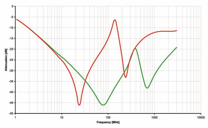
• Measurements carried out using galvanic coupling to             circuit indicates that some GND pins are related to
          certain ports to measure or inject RF signals                   certain VCC pins or ports, where decoupling caps are
                                                                          placed should take this knowledge into account. Ports
     Semiconductor companies have do deal mostly with                     that are connected on the outside of the ECU require
     testing at the IC level, however certain applications such           special attention – plan for decoupling capacitors to GND
     as automotive networking systems also require the proof              and series resistors if possible – 10 to 100Ω are often
     that some module level tests are passed by those ICs that            acceptable, whereas higher values will form a more
     include integrated bus line transceivers. The “classic”              efficient filter but also cause a higher voltage drop for
     EMC tests at the IC level measure the emissions in varying           DC signals. If emission of a particular port is the problem,
     frequency bands at defined frequency steps, dwell times,             one end of the resistor is connected to the port while
     measurement bandwidths and detector types as well                    the capacitor is on the other side. To protect a port
     as measuring immunity by applying an unmodulated                     against RF distortions the components are arranged
     or AM-modulated RF signal of defined amplitude, again                inversely. For frequencies >10MHz ferrite beads may be
     while varying the frequency at defined steps. These tests            more efficient than only utilizing small resistors and as a
     are specified in the international standards IEC 61967 for           further benefit their DC resistance is negligible, meaning
     emission and IEC 62132 for immunity. Currently these                 the circuit will not suffer from a drop in voltage.
     standards are supplemented by new test standards for pulse         • For higher frequencies a capacitor functions not only as
     measurements.                                                        a capacitor but also has some inherent, built-in parasitic
                                                                          components such as series inductance and resistance –
     Most ports at the IC level are designed to be connected              known as equivalent series resistance (ESR) – to name
     internally on the PCB only while just a few ports, such              only the most important components with adverse
     as supply pins, bus lines or antenna pins, are connected             effects. Because the correct choice and placement of
     externally. While EMC requirements are less stringent for            decoupling capacitors is of vital importance, this will be
     local (internal), the global (external) ports are far more           discussed in more detail below.
     critical because the cable lengths involved increase the
     cross-coupling between different lines or may behave as an         • In addition, resistors need to be regarded as a more
     undesired antenna for RF signals. Certainly a few ports such         complex component (highly depending on the type
     as those for bus lines are external ports by definition, but for     of construction and also on the resistance value).
     most ports it is the application that determines whether they        Fortunately, for a typical low-ohmic thin film resistor as
     need to be treated as local or global ports.                         they are used for building EMC filters, the contribution of
                                                                          its parasitic components is largely negligible up to 1GHz.
     The good news is that designing circuits and board layouts
     which are robust will not only ensure an assembly works            • When developing the PCB layout, the different circuit
     better and is more dependable but in most cases also                 blocks should be arranged in such way that sufficient
     help to achieve the required performance regarding both              space around sensitive inputs is provided towards
     electromagnetic emissions and immunity. Having said this,            switched signals of high amplitude and/or frequency
     how can circuit design be achieved which is that robust? Of          because of the possible interferences these signals may
     course there are a few general rules which help to improve           cause. Having parallel tracks on a board provides good
     the EMC behavior of the circuit:                                     coupling between the signals on these tracks – if this
                                                                          kind of coupling is not desired, insert some GND area
        • Careful consideration should be given to what clock             between the tracks; should these tracks cross each
          frequency is really needed for the development                  other at different layers, have the tracks cross at right
          application. The lowest clock frequency possible should         angles to minimize the coupling area. Keep tracks as
          be chosen because this is the first measure which will          short as possible, especially those carrying RF or
          reduce electromagnetic emissions.                               switched signals with fast slopes. Critical parts of the
                                                                          circuit such as tuners may require shielding. The highest
        • High-impedant ports are susceptible to RF distortions;          frequency the circuit produces or is exposed to should
          therefore, impedance should be kept as low as                   be considered and the track length of critical
          acceptable or a low-impedance path to GND for the               connections kept below 1/10 of the wavelength. Two
          RF disturbance should be provided. If an integrated             considerations must be kept in mind here: First, the

37                                                                                                                © 2010 / www.atmel.com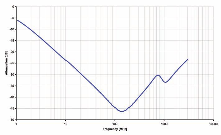
wavelength λ on the PCB is shortened due to εr of the                             Capacitor          ESR            Parasitic Inductance
             board material, for FR4 this is typically around 4.5;
             however the effective εr will be somewhat lower
             because part of the electric field of a micro strip line is in                                                 Cp
             free space. For a frequency of 3GHz the formula

                                                                                                                            Rp
             reveals that a track length of about 50mm already                Figure 1. Equivalent Circuit of a Capacitor
             equals λ/10.

             Secondly, the highest frequency in the circuit is
             determined by the   fastest slopes
                              Capacitor     ESR – soParasitic
                                                     if some     parts of
                                                              Inductance
             the design operate at 1MHz but with slopes of 1ns,                                                Resistor          Parasitic Inductance
             there will be frequencies of at least 500MHz on the
                                                  Cp
             PCB.
                                                                                                                   Cp Shunt Capacitance
           • Differential signals must be routed close to each
             other with the same track length for both lines. Avoid
             generating large loops and keep theRppath for the return
             current in mind. The larger the area of a loop, the higher       Figure 2. Equivalent Circuit of a Resistor
             the susceptibility and the lower the frequencies which
             may impact the circuit. Analogously, this is valid for
             emission, too – any tracks forming a loop with an RF             Equivalent Circuit Model of the Capacitor
             current flow can behave like a loop antenna.
                                                                              In the capacitor’s equivalent circuit model, the simplest model
           • The ground plane should be designed as solidly as                comprises just a serial connection of the nominal capacitor, an
             possible, preferably using a multilayer PCB with                 equivalent series resistance and a parasitic series inductance.
             dedicated layers for GND and power planes. Typically,            The ESR determines the lowest impedance reached at the
             the signal layers will be on the top and bottom side of          capacitor’s series resonance. Above this series resonance
             the PCB and the GND/power planes on the inner layers.            the capacitor’s impedance will increase with frequency,
             It is advantageous to keep the distance between signal           thus behaving like an inductor. A more sophisticated model
             layer and adjacent GND/power plane to a minimum.                 would also include the components Cp and Rp, connected in
             Doing so helps achieve relatively low track impedance            gray in Figure 1. Modified equivalent circuits are also found
             even for fairly thin connections. Slots in the GND plane         in literature which show Cp and Rp in parallel to the whole
             should be avoided to prevent creating unwanted slot              serial connection of (desired) capacitor, ESR and parasitic
             antennas. In addition, small “islands” should be avoided,        inductance; it is merely a question of transforming the
             different GND areas need to be connected using a                 values of the respective inherent components. The parasitic
             sufficient number of vias (one via every 3 to 5mm is             inductance together with Cp leads to a parallel resonance that
             sufficient for most designs).                                    is frequently neglected, because such parallel resonance of
                                                                              typical SMD ceramic capacitors will only appear at several
           • Hopping between the layers should be kept to a                   GHz.
             minimum during board development. Every via,
             especially “long” ones from top to bottom layer, involve         The series resonance of the capacitor is determined by its
             some inductance; as a rule of thumb this is in the range         type (electrolytic, foil, ceramic), mechanical dimensions
             of 0.5 to 1nH. Particular care needs to be taken about           (axial, radial, SMD, size) and of course its value. The higher
             GND connections of decoupling capacitors. Atmel® highly          the capacitance of a certain capacitor type, the lower the
             recommends placing several vias in parallel close to the         series resonance frequency. Therefore, it is advisable not
             respective capacitor.                                            just to place a single capacitor for decoupling purpose,
                                                                              but combine two or several caps to achieve broadband
                                                                              decoupling. For example, it is often recommended to pair a

Automotive Compilation Vol. 7                                                                                                                           38
Figure 3. Attenuation of two Ceramic Capacitors of 10nF and 100pF in
Parallel in a 50Ω System
10nF capacitor for lower frequencies with a 100pF cap for above 100Ω for 2-layer boards (1.6mm standard thickness)
higher frequencies. The following will explore whether this is will result and close to 50Ω will result for a multilayer board
advisable. A very basic linear RF simulation tool is sufficient for with 150μm distance between signal layer and GND plane.
demonstrating this; there are even freeware tools available
When considering the red curve in Figure 4, it is obvious it
for this purpose. Many manufacturers of ceramic capacitors
looks quite different from the previous graph. Figure 4 shows
supply S-Parameter files for their products and it is advisable
how decoupling performance changes if the board layout is
to use them. Figure 3 shows the attenuation of the above two
not done with care. The assumptions for the red curve were
capacitors when placed in parallel from a 50Ω track to GND.
as follows: standard 2-layer PCB, distance between caps and
This looks quite acceptable. Attenuation of at least 30dB to their GND vias: 10mm with just one GND via per cap. Now,
was achieved for frequencies between 20MHz and well quite unexpectedly, there is a highly undesirable resonance
above 1GHz. If a higher reference impedance than 50Ω around 130MHz with attenuation of only 6dB. The green
had been used, it would look even better. In a rather ideal graph in Figure 4 shows the performance for an improved
world, it would be possible to stop here. But has something board layout. Now a multilayer board is used, the two caps
been overlooked? In reality, it is not possible to connect are closer to each other and each one has two GND vias only
the capacitors perfectly to GND or to the track or pad 1mm away from the respective cap. The resulting decoupling
which needs to be decoupled. Every track on the PCB performance is significantly improved, but there still seems to
above behaves like a transmission line and its impedance be room for improvement.
is determined primarily by track width, the thickness of the
PCB or, in case that a multilayer PCB is used, the distance The lesson learned from this example is, first, the decoupling
between signal and GND layer, the distance to adjacent GND caps need to be as close as possible to each other and to the
areas and the dielectric constant εr of the PCB material. Again, component which needs to be decoupled. Secondly, using a
there are special books and free calculation tools available for multilayer PCB with a GND plane just below the signal layer
guidance on this issue. With track widths of 0.2mm, GND area is beneficial too. And, finally, it appears to be a good idea to
>0.5mm away from the track and εr = 4.7, impedance of well do some simulation with “real” capacitors rather than just
39 © 2010 / www.atmel.comRed: Distance between caps and their
GND vias: 10mm, one GND via per cap,
track width: 0.2mm, board thickness
top to GND: 1.6mm.
Green: Optimized, distance between
caps: 5mm, between caps and their
GND vias: 1mm, two GND vias per cap,
track width: 0.2mm, board thickness
top to inner GND plane: 0.15mm
Figure 4. Attenuation of two Ceramic Capacitors of 10nF and 100pF in Parallel in a 50Ω System with Realistic Parasitic
Components in Connecting Tracks
selecting them based on instinct. Innovative layout designs this becomes immediately noticeable on the connected
even place only a single centralized group of capacitors to receiving instrument. If the design performs weakly in terms
decouple a larger area – but that is something which should of susceptibility, consideration must be given to what parts of
not be attempted without careful simulation. the circuit are affected (this can often be deduced from the
malfunction occurring during the immunity measurement),
As mentioned previously in this article, car manufacturers
and the coupling path must be located. Once the critical
are aware that EMC issues generally become costlier the
parts of the circuit have been pinpointed, the techniques
later they are discovered. Engineers may benefit from this
described above can be used to improve EMC performance.
insight within their own development work. Giving some
A key consideration in this regard is that effective decoupling
thought to EMC behavior already when designing a circuit
requires a solid GND area. If this is lacking, it may be easier to
definitely helps avoid unpleasant surprises during EMC
redesign the board first; alternatively some copper foil could
approval testing. Having said that much – what needs to be
be added to facilitate further optimization measures in the
done if a design fails EMC testing despite the care exercised
lab.
prior to testing? Or, just in case it was not possible to include
sufficient time, budget or experience appropriate for EMC Hopefully it has become apparent that there is nothing
assessment in a project, what can be done to improve magical at all about EMC and that it is simply applied physics.
matters? Naturally, our knowledge about coupling mechanisms
and particularly their parameters tends to be inaccurate
The truth is that no standard procedure exists. If emission and sometimes incomplete, even if highly sophisticated
is the problem, a probe across the circuit can be attempted electromagnetic simulation tools are used. So there is a trace
with a field probe to detect any potential “hot spots.” Or, of magic (or uncertainty) left in the process after all. But
if fast enough, it is possible to re-perform the particular these imponderables are also what challenge us daily in this
failed emission measurement while connecting a short specialized discipline.
isolated wire to some “suspicious” spots on the PCB. If a
critical one shows up, the number of spurs will increase;
Automotive Compilation Vol. 7 40You can also read