FOR MICRO ELECTRO MECHANICAL SYSTEMS (MEMS)
←
→
Page content transcription
If your browser does not render page correctly, please read the page content below
SME MicroManufacturing Conference & Exhibits, Oakbrook Terrace, IL, April 2011

    BATCH MODE MICROMANUFACTURING BASED ON MICRO ELECTRO-DISCHARGE
               MACHINING AND MICRO ULTRASONIC MACHINING
             FOR MICRO ELECTRO MECHANICAL SYSTEMS (MEMS)
                                       Tao Li* and Yogesh B. Gianchandani
                         Engineering Research Center for Wireless Integrated Microsystems
                                   University of Michigan, Ann Arbor, MI, USA
                          ABSTRACT                                        compatible micromachining technologies capable of
                                                                          handling broader range of bulk materials remain highly
     Metal alloys have material properties that are very
                                                                          desirable.
appealing for micro electro mechanical systems (MEMS),
but present a challenge for process integration within a                       One category of bulk materials of interest is high
lithographic manufacturing sequence of the type used in the               strength and refractory metals and alloys such as steel,
semiconductor industry. The batch-mode micro electro-                     titanium (Ti), and platinum-rhodium (Pt-Rh). Steel has
discharge machining (µEDM) discussed here uses                            played important roles in macro-scale applications, but has
lithographically-fabricated electrode arrays with high                    not been explored for use in MEMS. Ti is well recognized
density and high uniformity to achieve high-throughput and                for its biocompatibility and has been used for packaging in
high-precision micromachining. It has been demonstrated                   implantable devices such as pacemakers, but in the MEMS
for potential applications that range from micro-gears to                 field it has been primarily used in thin films. Pt-Rh has a
smart stents.     Similarly, batch-mode micro ultrasonic                  proven history in chemically harsh environments but not for
machining       provides     lithographic      manufacturing              MEMS. These constraints can be addressed by batch-mode
compatibility to micromachining hard ceramics and other                   micro electro-discharge machining (μEDM) [1]. This is a
dielectric materials, such as glass-mica ceramic, lead                    lithography-based bulk-micromachining technology that can
zirconate titanate (PZT), single-crystal quartz, ruby, etc. In            handle any conductive materials, including metals and
this process, batch-µEDM is used to define a cutting tool                 alloys.
with desired pattern, typically in stainless steel. This has
                                                                               Another important category of bulk materials is
been demonstrated for the batch fabrication of piezoelectric
                                                                          ceramics, which in broad definition refer to any non-
transducers for smart biopsy tools and structurally complex
                                                                          metallic and non-organic solid materials. Ceramics offer
microresonators.
                                                                          important properties such as high electrical and thermal
                                                                          insulation, high melting temperature, and high chemical
                     I. INTRODUCTION
                                                                          stability. Piezoelectric ceramic materials, such as lead-
     In the last several decades, the emergence and rapid                 zirconate-titanate (PZT), have been widely used in sensors
development of micro electro mechanical systems (MEMS)                    and actuators. However, in the MEMS area PZT has mostly
have largely relied on established semiconductor                          been used as deposited thin film, which compromises
manufacturing technologies for integrated circuits (IC).                  material properties. Although there are already subtractive
Micromachining processes for silicon have been extensively                technologies that can process ceramics for MEMS
used for fabrication of MEMS sensors and actuators. The                   applications, there are limitations. For example, plasma
lithography-based batch manufacture of these devices has                  etching methods, such as reactive ion etching (RIE), have
allowed high throughput and low cost, and monolithic                      limited etching rate and require different gas chemistry for
integration with microelectronic circuits for increased                   different ceramics. Lithography-based pattern transfer to
functionality and performance. However, these machining                   ceramics still remains a challenge. Ultrasonic machining
processes generally favor silicon, some polymers and thin                 (USM), which is a highly effective technology for any hard
films of select metals and dielectrics. The means to add                  and brittle material, can be a promising candidate. At the
bulk materials are limited, particularly for metal alloys.                micro scale, it has mostly been used in serial mode, limiting
Electroplating is typically restricted to gold, copper and                its throughput and capability to handle complex patterns.
nickel. Other additive processes such as micromolding of                  Batch-mode micro ultrasonic machining (μUSM) process
ceramics can have issues of volume shrinkage and non-                     provides the capability of lithographic pattern transfer on
uniform material properties, especially at the micro scale.               any hard and brittle materials including ceramics and
In contrast, subtractive processes on bulk materials offer                glasses [2].
superior control of material properties and uniformity. Lack
                                                                               In the following sections, the details of batch mode
of diversity in bulk material choices for device structures
                                                                          µEDM and batch mode µUSM will be described and some
has limited the functionality and performance of many
                                                                          of the applications to date will be presented.
MEMS devices, and often impedes the development of new
and potential MEMS applications. Thus, lithography

*
Corresponding author: 1301 Beal Ave., Ann Arbor, MI, 48109, USA; Tel: 1-734-615-7983, Fax: 1-734-763-9324, Email: litz@umich.edu
                                                                                                                                     1
SME MicroManufacturing Conference & Exhibits, Oakbrook Terrace, IL, April 2011
II. BATCH MODE µEDM
The μEDM process can be used to machine 3D
microstructures from any electrically conductive material,
including steel, graphite [3], silicon [4], and magnetic
materials such as permanent magnets [5]. When combined
with lithography technology, μEDM can be used in batch
mode, providing high spatial density, high uniformity, and
much higher throughput compared with serial mode μEDM
[1].
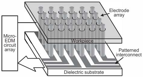
Overall Process Description Fig. 1: Concept of batch mode μEDM with single pulse generating
The µEDM process involves the sequential discharge circuit [1].
of electrical pulses between a microscopic electrode and the
controlled, it is possible to achieve both spatial and
workpiece while both are immersed in dielectric oil [6].
temporal multiplicity, providing machining throughput that
The pulse discharge timing is controlled by a simple RC
is orders of magnitude higher than is possible by a serial
circuit. The electrode is conventionally a cylindrical metal
approach. This is referred to as parallel discharge. It can be
element that has a minimum demonstrated diameter of ≈5
facilitated, in part, by utilizing the parasitic on-chip
μm. The electrodes can be individually shaped by using a
capacitance between the electrodes and the Si substrate as a
μEDM technique known as wire electro-discharge grinding
design component within the pulse timing circuit. Not only
(WEDG) [7]. The use of a single electrode that is scanned
does this provide a compact solution, but the resulting
or scrolled across the sample surface for machining is
elimination of the parasitic nature of the capacitance
referred to as the serial mode µEDM. A typical machine for
provides superior control over the size and timing of the
this purpose was originally developed by Panasonic, Inc.
pulses, improving the precision of the machining and
Enhanced models are now available from SmalTec, LLC.
reducing crosstalk between electrodes. Using this mode of
In order to achieve micron-scale precision, the apparatus
operation, a throughput >100× higher than that of serial
uses an extremely small amount of discharge energy (10-7 J
μEDM with a single electrode has been demonstrated [1].
level) and submicron accuracy in spindle rotation, feeding,
and positioning. Submicron tolerance and fine surface With the introduction of the batch mode concept, the
finish of 0.1 μm Rmax roughness have been demonstrated [6]. shaping capability, feature density, throughput, and
uniformity of μEDM technology has been greatly improved.
Although it has been commercially used for
Although it is not suitable for machining dielectric materials,
applications such as ink-jet nozzle fabrication, the serial
the capability of EDM to handle hard metals such as tool
μEDM method is limited in throughput. This is especially
steel and WC/Co makes it an attractive technique for
true for complex patterns such as gears, which require
preparing cutting tools which can be used to mechanically
contour scanning along the edge of the patterns. Batch
machine dielectrics. This is discussed in Section III.
mode μEDM, which uses lithographically-fabricated
electrode arrays, can overcome this limitation [1,8]. The Tackling the Debris Buildup Issue
concept is shown in Fig. 1. By using precisely located high- During the µEDM process, debris accumulation
aspect-ratio electrode arrays fabricated by lithography and between the electrode and workpiece can lead to spurious
electroplating processes, the batch mode μEDM process can discharges that damage the workpiece surface and cause
provide not only high throughput but also high spatial excessive tool wear. In batch mode µEDM, this can
density and uniformity over the whole machining area. become even more serious due to the large area and small
Electroplated copper is used as the electrode material separation of the tool from the workpiece, and can cause
because it has high melting point and high thermal uncontrolled arcing and stall the machining indefinitely. A
conductivity for minimized wear of the electrodes. The parametric study of the batch mode μEDM of high density
LIGA process, which is the German acronym for features in stainless steel confirmed that, when the tool
lithography, electroplating, and molding, can be used to feature density is increased, the effect of debris
form exceptionally high-aspect-ratio molds for accumulation begins to dominate and eventually degrades
electroplating by deep X-ray lithography [9]. During both tool and workpiece [10]. Two independent techniques
machining, the whole electrode array (cathode) is fed into for mitigating this debris buildup have been proposed [10].
the workpiece (anode); discharges are fired and the whole The first is a passivation coating which suppresses spurious
pattern is transferred onto the workpiece [1]. discharges triggered from the sidewalls of the machining
tool. By this method, the mean tool wear rate decreases
The array of electroplated Cu electrodes fabricated on a
from a typical of about 34% to 1.7% and machining non-
carrier substrate provides spatial multiplicity in the
uniformity reduces from 4.9 μm to 1.1 μm across the
electrical discharges. However, if the electrodes are all
workpiece. The second technique involves a two-step
connected in parallel to the same pulse generation circuit,
machining process that enhances the hydrodynamic removal
only one tends to fire at any given moment. By separating
of machining debris compared to standard methods. By
arrayed electrodes into segments that are independently
2SME MicroManufacturing Conference & Exhibits, Oakbrook Terrace, IL, April 2011
first µEDM’ing narrow through-holes in the workpieces at
selected locations across the machining area, a path is
created for the debris to escape when the overlaid, final
pattern is machined. This improves surface and edge finish
of the machined features, machining time and tool wear.
Wireless Process Monitoring
Traditional methods of monitoring EDM machining
quality rely on electrical characteristics at the discharge
supply terminals. Inherent wireless signals generated with
each discharge in μEDM can be used for direct observation
of discharge quality. This wireless method is less affected
by electrical parasitics in the supply loop and by spatial
averaging. This approach has been shown to help address
two significant challenges in µEDM: sensing a material
transition within a workpiece, and sensing excessive debris
accumulation [11]. The depth location of a metal-metal Fig. 2: LEEDUS process utilizes lithography, electroplating, and
interface can be distinguished in the wireless signal. This is batch mode µEDM to fabricate a microtool with a pattern which is
useful for determining the stop depth in certain processes. defined by a mask, and then uses batch mode µUSM to transfer the
For example, in machining through samples of stainless pattern onto ceramic or other brittle materials. Non-lithographic
steel into an electroplated copper backing layer, the metal rapid-prototyping can also be performed for simple patterns using
option 2 (SEDUS) [2].
transition is identified by a 10-dBm change in wireless-
signal strength for a 300-350 MHz band and a 5 dBm be formed using SU8 or LIGA molds with lithographically-
average change across a full 1 GHz bandwidth. This can be defined patterns. These copper structures are then used as
applied to separate stacked metals as well. As debris an electrode for batch µEDM to transfer the patterns onto
accumulate in the discharge gaps, shifts in the wireless hard metal substrates for microtools. Non-lithographic
spectra can also indicate spurious discharges that could rapid-prototyping can be performed for simple patterns by
damage the workpiece and tool. For example, when copper the original serial function of a Panasonic/SmalTec µEDM
micromachining becomes debris dominated, an 800-850 machine. A program on a computer controls the “writing”
MHz band drops 4 dBm in signal strength, with a 2.2 dBm movement of the rotating µEDM electrode on the microtool
average drop across a full 1 GHz bandwidth. substrate as well as different cutting depths for multi-level
structures.
III. BATCH MODE µUSM The microtool is then mounted on a custom-built setup
Conventional USM has been widely accepted as an for batch mode µUSM, and the patterns on the microtools
effective machining process for hard and brittle materials are transferred onto a ceramic workpiece. Abrasive slurry,
like ceramics, glass, etc. These materials are brittle and are which consists of water and fine abrasive powders, is
more easily fractured than plastically deformed. Hence, supplied between the tip of the microtool and the workpiece.
USM produces little or no damage or high-stress The vibrating tip of the microtool is fed into the workpiece.
deformation at or below the surface. Moreover, it causes no The ultrasonic motion of the microtool imparts velocity to
thermal or chemical alterations in the sub-surface the abrasive particles on its downward stroke. These
characteristics of the machined material [12]. However, particles, in turn, are responsible for the erosion of the
USM at the micro level has been mostly utilized in a serial workpiece, thus creating the desired cavities in the shape of
approach with a single rotating tool, limiting both the microtool.
throughput and structural shapes [13,14]. The batch mode Both dynamic force detection and acoustic emission
µUSM approach facilitates parallel transfer of complex (AE) detection have been used to monitor the µUSM
lithographic patterns and provides relatively high resolution process [2,15]. The dynamic force detection approach uses
and throughput, while retaining the favored characteristics wideband piezoelectric sensors and can be used to directly
of conventional USM [2]. measure the machining load. In contrast, the AE sensor
Overall Process Description detects the higher-frequency transient elastic waves
A candidate process flow is shown in Fig. 2. First, generated by microchipping that occurs in the workpiece
hard-metal (e.g. steel) microtools with desired patterns are during µUSM, while filtering out the main frequency
made by micro electro-discharge machining (µEDM). This component of vibration from the ultrasound generator. This
can be performed in batch mode for compatibility with provides an effective measure of the actual machining.
lithographic methods (LEEDUS) [1], or serial mode for Batch-mode µUSM has been successfully applied to
rapid prototyping of simple patterns (SEDUS). Multi-level Macor® glass ceramic [2], PZTs [2,], single-crystal quartz
structures can also be defined in the microtools [15]. For [15], Zerodur® [15], ruby and glasses [16], etc. Feature
batch mode operation, electroplated copper structures can sizesSME MicroManufacturing Conference & Exhibits, Oakbrook Terrace, IL, April 2011
to make an array of shallow spherical cavities. Separately-
manufactured fused quartz spheres are then embedded into
these cavities, allowing self-alignment between the tool
steel spheres and the target fused quartz spheres. Finally, a
second batch-mode µUSM step is done with the same tool
to form the mushroom (Fig. 3d) or concave (when no holes
are made into the tool spheres) geometries. Since µUSM
does not involve any chemical or high temperature steps, it
is possible to create stress-free structures in a wide variety
of ceramics, glasses and other brittle materials.
IV. APPLICATIONS
The µEDM and µUSM processes have been applied to
the implementation of a variety of MEMS sensors and
Fig. 3: Schematic of the (a) mushroom and (b) concave shaped actuators. Several examples of the demonstrated
spherical structures fabricated using the 3D-SOULE process. (c)- applications are presented in this section.
(d): Process illustration for the mushroom structure [16].
Batch Microfabricated Gears
depths >350 µm and cutting rates >24 µm/min. have been Using the parallel discharge approach in batch mode
demonstrated. µEDM, a monolithic partitioned electrode array with
3D Micromachining of Spherical Geometries multiple pulse generating circuits was fabricated by a two-
Three dimensional (3D) microstructures in hemispheric, mask sacrificial LIGA process (Fig. 4a) [1]. This electrode
“wine glass” and mushroom shapes (Fig. 3a-b) made from array had 10 μm wall thickness and 300 μm height. It was
high quality factor (Q) materials, e.g. fused quartz, are used to fabricate gears (Fig. 4b) from 70 μm-thick tungsten
attractive for some types of inertial sensors, such as rate carbide cobalt (WC/Co) super hard alloy plates. Using the
integrating gyroscopes [17,18]. However, these materials electrode array provided throughput more than 100 times
cannot be easily micromachined into 3D geometries with higher than that of serial μEDM using a single electrode.
either conventional lithography-based technologies or Stents and Antenna Stents
melting/reflow, and are difficult to integrate with silicon or The μEDM method has been used in the recent past to
other substrates. A lithography-compatible method for fabricate stents [19,20]. Stents are mechanical devices that
integrating and micromachining concave and mushroom- are chronically implanted into arteries in order to physically
shaped spherical structures made from these materials has expand and scaffold blood vessels that have been narrowed
been developed. The 3D-SOULE process [16] is a 3D- by plaque accumulation. Although they have found the
capable and self-aligned process combining batch-mode greatest use in fighting coronary artery disease, stents are
μUSM, lapping, and μEDM. The tool is prepared by also used in blood vessels and ducts in other parts of the
embedding separately-manufactured high-grade steel body. These include iliac, carotid, and renal arteries, biliary
spheres onto a steel substrate with µEDM’ed cavities, to ducts and ureters. The vast majority of coronary stents are
form an array of spherical features for batch machining (Fig. made by laser machining of stainless steel tubes, creating
3c). Holes can also be made into the steel spheres to form mesh-like walls that allow the tube to be expanded radially
the stems of the target mushroom structures. The tool is with a balloon that is inflated during the medical procedure,
then used in batch-mode µUSM of a silicon carrier substrate known as balloon angioplasty. A lithography-compatible
method for fabricating these devices would be useful for the
purpose of integrating sensors and sensing materials onto
them. (It would also permit such 3D structures and
assembly methods to be incorporated into the portfolio of
micromachining techniques being used for other devices.)
This type of ability to monitor pressure and flow can be
useful because re-narrowing (restenosis) often occurs
following a stenting procedure, and intraluminal wireless
sensors for pressure or flow can be used in monitoring of
the patency of the lumen.
A lithography-compatible approach can be used for
machining stents and other tubular meshes without the need
for bonded or welded seams [19]. The patterns, such as
involute bands between a pair of side-beams, are cut into
Fig. 4: (a) Monolithic copper electrode arrays with patterned
50-μm thick stainless steel foil. In assembling the device, a
interconnect. (b) WC-Co super hard alloy gears batch-cut from a
70-µm thick workpiece using electrode arrays shown in (a) [1]. deflated angioplasty balloon is threaded alternately above
4SME MicroManufacturing Conference & Exhibits, Oakbrook Terrace, IL, April 2011
Fig. 6: Photograph of the tissue contrast sensing microsystem
(a) using piezoelectric sensors with integrated analog CMOS interface
circuits [25].
Biopsy Tools
The ability of μEDM to pattern steel has also been
useful in embedding micro-scale transducers into biopsy
tools. The machining capability of µUSM on piezoceramics
has been employed to form transducers for these
(b) applications. The work described in [22-25] was initially
Fig. 5: (a) Stent fabricated from planar steel foil using μEDM and motivated by fine needle aspiration (FNA) of thyroid
deployed within a mock artery using balloon angioplasty [19]. (b) nodules. FNA biopsy is a common clinical procedure for
The antenna stent coupled with two capacitive pressure sensors harvesting cells from the thyroid, breast, etc. for subsequent
[20]. cytological examination. It is typically performed with 20-
and below the bands, and then expanded by a normal 27 gauge needles, with outer diameterSME MicroManufacturing Conference & Exhibits, Oakbrook Terrace, IL, April 2011
can address the issues encountered with the passive device.
It also eliminates the requirement of readout equipment
such as the impedance analyzer, so that this technology can
be potentially low-cost and widely accessible. A sensor
element and CMOS circuit have been fabricated in-house at
the University of Michigan, and integrated onto the tip of a
20-gauge biopsy needle. The sensor module with integrated
interface circuit has a size of 950 µm (L) × 350 µm (W) ×
220 µm (H). At this time, preliminary functional
verification has validated the sensing system design.
Ongoing efforts are directed at testing and performance
evaluation of the microsystem, as well as tissue loading
measurements in single and differential mode operation. Fig. 7: (Upper two) Microtools made from stainless steel using
Although percutaneous biopsies are generally safe, µEDM; (Lower two) microstructures with multiple structural
levels made from single-crystal quartz by batch mode µUSM [15].
potential risks include the deposition of viable tumor cells
along the needle tract, and post biopsy hemorrhage. Zerodur®, has also been micromachined at a cutting
Cauterization of needle tracts is known to minimize these rate >18 µm/min.
risks. A method for cauterization of the needle tract was
reported in [23]. In this method, an array of 200 µm- In conclusion, it is evident that batch mode µEDM and
diameter PZT disks was integrated at the tip of a 20-gauge batch mode µUSM can expand the bulk material options for
biopsy needle. These PZT discs were used as heaters and lithographically machined microstructures. While
generated a temperature rise of 33°C with an input power of additional work is needed to make these processesSME MicroManufacturing Conference & Exhibits, Oakbrook Terrace, IL, April 2011
on Micro Electro Mechanical Systems (MEMS '90), Napa [17] A. Matthews, and F.J. Rybak, “Comparison of hemispherical
Valley, California, pp. 21-26, February 1990 resonator gyros and optical gyros,” IEEE Aerospace and
[7] T. Masuzawa, M. Fujino, K. Kobayashi, T. Suzuki, N. Electronic Systems Magazine, 7, pp. 40-46, 1992.
Kinoshita, “Wire Electro-Discharge Grinding for Micro- [18] A.M. Shkel, C. Acar and C. Painter, “Two types of
Machining,” Ann. CIRP, v. 34, pp. 431-434, 1985 micromachined vibratory gyroscopes,” IEEE Sensors, pp.
[8] K. Takahata, N. Shibaike, and H. Guckel, "A novel micro 531-536, 2005.
electro-discharge machining method using electrodes [19] K. Takahata and Y.B. Gianchandani, “A Planar Approach for
fabricated by the LIGA process," in Proc. IEEE Int. Conf. Manufacturing Cardiac Stents: Design, Fabrication and
Micro Electro Mechanical Systems (MEMS 1999), Orlando, Mechanical Evaluation,” IEEE/ASME Journal of
FL, Jan. 1999, pp. 238-243. Microelectromechanical Systems, 13(6), pp. 933-939, Dec.
[9] H. Guckel, “High-aspect-ratio micromachining via deep X- 2004
ray lithography,” Proc. IEEE, vol. 86, no. 8, pp. 1586-93, [20] K. Takahata and Y.B. Gianchandani, K.D. Wise,
Aug. 1998 “Micromachined Antenna Stents and Cuffs for Monitoring
[10] M.T. Richardson and Y.B. Gianchandani, "Achieving Intraluminal Pressure and Flow,” IEEE/ASME J.
Precision in High Density Batch Mode Micro-Electro- Microelectromechanical Systems, 15(5), pp. 1289-1298,
Discharge Machining," IOP Journal for Micromechanics and October 2006
Microengineering, vol. 18, no. 1, 015002 (12 pp.), January [21] M.A. Fonseca, M.G. Allen, J. Kroh, J. White, “Flexible
2008 wireless passive pressure sensors for biomedical
[11] M. Richardson, Y.B. Gianchandani, “Wireless monitoring of applications,” Solid-State Sensors, Actuators and
workpiece material transitions and debris accumulation in Microsystems Workshop (Hilton Head ’06), S. Carolina, June
micro-electro-discharge machining,” IEEE/ASME J. '06, pp. 37-42
Microelectromechanical Systems, 19(1), pp. 48-54, February [22] T. Li, R. Y. Gianchandani, and Y. B. Gianchandani,
2010 "Micromachined bulk PZT tissue contrast sensor for fine
[12] T.B. Thoe, D.K. Aspinwall, and M.L.H. Wise, “Review on needle aspiration biopsy," Lab on a Chip, vol. 7, no. 2, pp.
ultrasonic machining,” International J. Machine Tools & 179-185, Feb. 2007.
Manufacture, vol. 38, no. 4, pp. 239-255, Apr. 1998 [23] K. Visvanathan, Y.B. Gianchandani, “Biopsy Needle Tract
[13] X. Sun, T. Masuzawa, and M. Fujino, “Micro ultrasonic Cauterization Using and Embedded Array of Piezoceramic
machining and its applications in MEMS,” Sensors and Microheaters,” IEEE/ASME International Conference on
Actuators A (Physical), vol. A57, no. 2, pp. 159-64, Nov. Micro Electro Mechanical Systems (MEMS 10), Hong Kong,
1996 Jan. 2010, pp. 987-1000
[14] H. Choi, S. Lee, and B. Lee, “Micro-hole machining using [24] K. Visvanathan, T. Li, and Y.B. Gianchandani, "In situ
ultrasonic vibration,” Key Engineering Materials, vol. 238- monitoring of cauterization with a biopsy needle using
239, pp. 29-34, 2003 impedance characteristics of embedded piezothermal
[15] T. Li and Y. B. Gianchandani, “A high speed batch mode elements," 14th Int. Conf. Miniaturized Syst. Chemistry and
ultrasonic machining technology for multi-level quartz crystal Life Sciences (μTAS 2010), Groningen, Netherlands, Oct.
microstructures,” IEEE International Conference on Micro 2010, pp. 1478-80
Electro Mechanical Systems, Hong Kong, pp. 398–401, 2010. [25] T. Li and Y.B. Gianchandani, "An active tissue-contrast
[16] K. Visvanathan, T. Li, and Y.B. Gianchandani, "3D-SOULE: sensing microsystem for biopsy needles: initial results," The
A fabrication process for large scale integration and 24th IEEE Int. Conf. Micro Electro Mechanical Syst. (MEMS
micromachining of spherical structures," The 24th IEEE Int. 2011), Cancun, Mexico, Jan. 2011, pp. 21-24
Conf. Micro Electro Mechanical Syst. (MEMS 2011), Cancun, [26] F. Pacini and L.J. De Groot, “Thyroid Neoplasia,” The
Mexico, Jan. 2011, pp. 45-48 Thyroid and its Diseases, 6th ed., W.B. Saunders Company,
1996, updated online at www.thyroidmanager.org, May 2004.
7You can also read