IMPACT OF RESIDUAL CARBON IMPURITIES AND GALLIUM VACANCIES ON TRAPPING EFFECTS IN ALGAN/GAN MIS-HEMTS
←
→
Page content transcription
If your browser does not render page correctly, please read the page content below
Impact of Residual Carbon Impurities and Gallium Vacancies on Trapping
                                                 Effects in AlGaN/GaN MIS-HEMTs
                                                         Martin Huber,1, 2 Marco Silvestri,1 Lauri Knuuttila,1 Gianmauro Pozzovivo,1 Andrei Andreev,1 Andrey
                                                         Kadashchuk,3, 4 Alberta Bonanni,2 and Anders Lundskog1
                                                         1)
                                                            Infineon Technologies Austria AG, Siemensstrasse 2, A-9500 Villach, Austria
                                                         2)
                                                            Johannes Kepler University, Institute of Semiconductor and Solid State Physics, Altenbergerstrasse 69,
                                                         A-4040 Linz, Austria
                                                         3)
                                                            IMEC, Kapeldreef 75, B-3001, Leuven, Belgium
                                                         4)
                                                            Institute of Physics, National Academy of Science of Ukraine, Prospekt Nauki 46, 03028 Kyiv,
                                                         Ukraine
                                                         Effects of residual C impurities and Ga vacancies on the dynamic instabilities of AlN/AlGaN/GaN metal
arXiv:2002.01952v1 [physics.app-ph] 5 Feb 2020

                                                         insulator semiconductor high electron mobility transistors are investigated. Secondary ion mass spectroscopy,
                                                         positron annihilation spectroscopy, steady state and time-resolved photoluminescence (PL) measurements
                                                         have been performed in conjunction with electrical characterization and current transient analyses. The
                                                         correlation between yellow luminescence (YL), C- and Ga vacancy concentration is investigated. Time-
                                                         resolved PL indicating the CN ON complex as the main source of the YL, while Ga vacancies or related
                                                         complexes with C seem not to play a major role. The device dynamic performance is found to be significantly
                                                         dependent on the C concentration close to the channel of the transistor. Additionally, the magnitude of
                                                         the YL is found to be in agreement with the threshold voltage shift and with the on-resistance degradation.
                                                         Trap analysis of the GaN buffer shows an apparent activation energy of ∼0.8eV for all samples, pointing
                                                         to a common dominating trapping process and that the growth parameters affect solely the density of trap
                                                         centres. It is inferred that the trapping process is likely to be directly related to C based defects.

                                                    The AlGaN/GaN material system is a fundamental              recent hybrid functional calculations, the VGa ON com-
                                                 building-block for the fabrication of high-power GaN on        plex is thought to have a maximum in the infrared (IR)
                                                 Si metal insulator semiconductor high electron mobil-          region.13 Recently, the YL band was attributed to elec-
                                                 ity transistors (MIS-HEMTs).1,2 Despite the large lattice      tron transitions from the conduction band minimum to
                                                 and thermal coefficient mismatch, Si is widely used as the     the corresponding transition levels of C substitution at
                                                 substrate of choice for nitride-based HEMTs. Complex           the N site (CN ) and at the CN ON complex.14 The effect
                                                 multilayer structures are needed in order to maintain the      of VGa concentration and possible related complexes in
                                                 strain during the growth, at the same time the structure       the epitaxial structure on dynamic instabilities of work-
                                                 should provide high electrical resistance and low leakage      ing devices has not been thoroughly investigated yet.
                                                 currents. One way to satisfy these requirements, is to            In this work, we report on the impact of buffer residual
                                                 introduce acceptor-like impurities, e.g. Fe or C [3 and        C impurities and Ga vacancies on the dynamic properties
                                                 4]. However, Fe is considered as non-suitable element          of AlGaN/GaN HEMT structures. We utilize a combi-
                                                 in the front-end-of-line Si area, limiting the integration     nation of complementary characterization techniques in
                                                 possibilities in low-cost environments. Carbon on the          order to understand the relationship between YL, impu-
                                                 other hand, could potentially fulfill the task as it acts as   rity concentrations, threshold voltage- and on-resistance
                                                 a source of donor compensation centers, while being Si         instabilities.
                                                 environment friendly. For efficient GaN based devices,            Four different AlGaN/GaN structures (A, B, C and D)
                                                 it is of uttermost importance to reduce, or avoid trap-        have been grown on Si(111) 150 mm substrates by metal
                                                 ping related failures such as current collapse, dynamic        organic vapor phase epitaxy in a multi-wafer AIXTRON
                                                 on-resistance (RDSON ) degradation and threshold volt-         planetary reactor. The epitaxial stack is sketched in Fig.
                                                 age (Vth ) shifts.                                             1(a). It consists of three parts, namely a highly resis-
                                                    The location of the traps causing dynamic instabili-        tive multilayer AlGaN/GaN structure grown on the Si
                                                 ties in the HEMT structure is still under debate. Some         substrate, a subsequent unintenionally doped (UID)-GaN
                                                 studies5,6 indicated that trapping occurs solely in the        layer and an AlGaN barrier overlayer. The thickness of
                                                 buffer due to C-doping, while others showed that the           the layers is 4500 nm, 500 nm and 20 nm, respectively.
                                                 trapping takes place at the interface between the dielec-      The AlGaN barrier overlayer and the UID-GaN layer
                                                 tric and the III-nitride semiconductor.7,8 Combinations        form the two dimensional electron gas (2DEG) channel of
                                                 of the two previously mentioned processes have also been       the HEMT structure. In this study, only the growth con-
                                                 proposed.9 A clear attribution of the yellow luminescence      ditions of the UID-GaN layer are systematically varied in
                                                 (YL) band around 2.2 eV in GaN-related materials sys-          order to achieve different impurity and vacancy concen-
                                                 tems to a single species or defect has been under discus-      trations. Since the variation of the growth conditions has
                                                 sion for long time.10 Previously, it has been argued that      also an effect on the growth rate, the overall UID-GaN
                                                 Ga vacancies (VGa ) accompanied by C or O could be             layer thickness has been kept constant by adjusting the
                                                 responsible for the YL band.11,12 However, according to        deposition times.
2
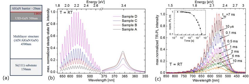
FIG. 1. (a) Sketch of the studied HEMT structure. (b) Steady-state PL spectra at room temperature showing YL as a broad
peak at ∼2.2 eV and the BE peak at ∼3.4 eV. The spectra are normalized to the maximum PL intensity of sample D. (c)
TR-PL spectra at room temperature for sample D. Inset: time dependence of the spectrally integrated YL band intensity
(squares), the solid line is a guide to the eye.
Secondary ion mass spectroscopy (SIMS) analysis has
TABLE I. Impurity- and VGa concentrations in the UID-GaN
been performed in a Phi-Evans quadrupole secondary ion
layer for samples A, B, C and D, respectively. The C and Si
mass spectrometry system equipped with Cs primary ion content is obtained from SIMS, while the VGa concentration
source operated at low range keV energy to determine from PAS measurements.
the impurity concentrations in the UID-GaN layer.
Sample C (1016 /cm3 ) Si (1016 /cm3 ) VGa (1017 /cm3 )
Room temperature positron annihilation spectroscopy
(PAS) is a widely used technique to determine the va- A 1.3 5.2 6.0
cancy concentration in various material systems. For this B 3.3 1.0 2.0
sample set, PAS analysis has been performed with a slow C 7.0 3.0 1.0
positron beam using acceleration energies between 1 keV D 12.4 1.0 0.8
and 25 keV. The VGa concentration has been determined
by analyzing the shape of the Doppler-broadened 511 keV
positron-electron annihilation energy peak.15 length is 1 µm, while the gate-source distance and the
The structures have been characterized by room tem- gate-drain distance are 1.5 µm and 12 µm, respectively.
perature photoluminescence (PL) measurements using a The rated breakdown voltage is 650 V at 10 nA/mm. The
HeCd laser for excitation with a wavelength of 325 nm devices are passivated by using SiN and poly-imide. Elec-
and a power density of 0.1 W/mm2 . Time-resolved pho- trical characterization includes various stress tests up to
toluminescence (TR-PL) measurements have been car- 600 V. For the threshold voltage shift, the devices have
ried out using a set-up consisting of a pulse UV-laser been subjected to a stepped OFF-state stress, keeping
(pulse width of 1.7 ns and pulse energy 300 µJ) for opti- the gate source voltage (VGS = -12 V) fixed. The stress
cal excitation at 355 nm and a monochromator coupled pulse duration is set to one minute and the drain voltage
to an intensified CCD camera with a time-gated, inten- to 600 V. The Vth and the static RDSON are measured
sified diode array detector, synchronized to the laser. A directly after applying the stress pulse. Double pulse
variable delay from 7 ns to 10 ms after laser pulse ex- measurements have been performed using an AMCAD
citation and a constant time gate width of 15 ms have double pulse system with a pulse length ton = 2 µs and
been used to obtain the TR-PL spectra. To increase the toff = 1 ms. Dynamic RDSON are extracted from pulsed-
signal-to-noise ratio, spectra have been collected by av- IV curves using different quiescent bias points at VGS
eraging over 200 pulses. = -20 V and the drain voltage is set to 200V. Transient
The material characteristics are correlated with the measurements have been carried out using a parameter
electrical performances of the MIS-HEMT devices analyzer equipped with a heated chuck allowing investi-
fabricated by using a complementary metalo-oxide- gations up to 150 ◦ C.
semiconductor (CMOS) production line. The 2DEG The results of the SIMS and PAS measurements for
sheet resistance is ∼460 Ohm/sq. Hall mobility and samples A, B, C and D are summarized in Table I. Sig-
2DEG density are 1800 cm2 /Vs and 7.5x10¹² 1/cm2 , re- nificant signals from C and Si are observed while signals
spectively. The Au-free ohmic contacts consist of a Ti/Al from O (∼1x10¹⁶ /cm3 ) and H (low 1017 /cm3 ) are close to
based metal stack with Rc =0.5 Ohm·mm. The gate (or below) the SIMS detection limits.16 The variation of3
17
1.3x10 17
6.10x10 75
V Carbon V shift (V =-12 V, V =600 V)
Ga th GS DS 90
R degradation (V =-20 V, V =200 V)
species concentration [1/cm ]
DSON GS DS
3
60 75
degradation [%]
17
4.70x10
16
9.0x10
shift [%]
60
45
17
3.30x10
45
th
16
DSON
V
5.0x10 30
17
1.90x10
R
30
15
15
16 16
1.0x10 5.00x10
A B
0 0
0.05 0.10 0.15 0.20 0.25 0.30 0.35
0.05 0.10 0.15 0.20 0.25 0.30 0.35
max. normalized yellow luminescence max. normalized yellow luminescence
FIG. 2. YL as a function of the C- and VGa concentrations. FIG. 3. Vth shift for a 600 V stressed device and RDSON for
Black squares: SIMS average C concentration in the UID- a 200 V stressed device measured with a double pulse setup.
GaN layer for each sample. Red dots: PAS VGa concentration
in the UID-GaN layer for each sample.
eV [14], while the CN ON complex generate solely the YL
band with a maximum at 2.2 eV. It is worth mention-
growth parameters is known to have a particularly large ing that the GL and YL have distinctly different decay
impact on the VGa and C concentrations.17 The change times of a few µs and a few ms, respectively. The TR-PL
in the VGa concentration is attributed to the different measurements presented in Fig. 1(c) do not show pres-
V/III molar ratios at the different growth conditions.18 ence of the GL band in sample D. This suggests that the
The samples in Table I are listed in order of increasing observed YL band in our samples is mostly dominated
C impurity concentration (from A to D). by emission from CN ON complexes rather than from iso-
In Fig. 1(b) the steady state PL intensity measured at lated CN defects. This conclusion is supported by the
room temperature in the UV-Vis range for the samples fact that (i) no short-live component expected for GL in
A, B, C and D is shown. The PL spectra at room tem- µs-time domain is actually observed in the measured de-
perature (RT) of all samples are dominated by a broad cay kinetics shown in the inset to Fig. 1(c), and that (ii)
YL band at around 2.2 eV (564 nm) and by the GaN the observed YL band has a maximum at 564 nm (2.2
band-edge (BE) emission peak at 3.4 eV (365 nm). The eV) and not at 590 nm (2.1 eV) as it would be expected
intensities of both YL and BE band emission are found to for CN defects.
vary significantly within the sample set. In order to com- In order to study the dynamic instabilities of the
pare the YL emission from the different samples, peak in- devices, the threshold voltage shift and the change in
tensity integration between 1.85 eV and 2.55 eV has been RDSON with the application of a high-voltage off-state
carried out. In Fig. 2 the YL area as a function of the C- stress pulse have been analyzed. Due to trapping pro-
and VGa concentration in the UID-GaN layers is plotted. cesses, Vth is shifted to more negative values and the
Remarkably, a linear correlation between the C concen- RDSON degradation is also changing towards higher val-
tration and the YL is observed, while the YL band in- ues with respect to initial measurement after applica-
tensity is in anti-correlation with the VGa -concentration, tion of the stress pulses. This behavior was recently at-
indicating that the YL is mainly originated by carbon- tributed to electron traps in the GaN channel that are
related defects or by carbon itself in the UID-GaN layer. emptied under measurement conditions and filled under
Indeed, C is generally expected to act as a deep acceptor stress conditions.9 Threshhold voltage shift and RDSON
with the (-/0) charge state transition level at ∼0.9 eV degradation are given in percentage of the initial values.
above the valance band maximum (VBM) when incorpo- In Fig. 3 the Vth shift and the RDSON degradation at
rated at a N site CN in the GaN lattice.19 The CN ON one representative stress level for each of the measure-
complex is a deep donor with the 0/+ level at ∼0.75 eV ments are given as a function of the YL band area. The
above the VBM [13]. The observed relationship between results reported in Fig. 3 show that the threshhold volt-
YL and C concentration is in agreement with a recent age shift and RDSON degradation increase with increasing
comprehensive study by Reshchikov et. al.,14 where it YL band intensity, in agreement with earlier studies.20
was found that (i) the CN defect and the CN ON complex We conclude that C-related defects, most likely CN ON
produce the yellow band and that (ii) neither isolated complexes, are the dominant factor for the dynamic in-
VGa nor related complexes can account for this band. stabilities of the final device. Therewith it is confirmed
Moreover, it was found that the isolated CN defect does that even at RT the monitoring of the YL is decisive
not only produce the YL band (maximum at 2.1 eV) but to predict dynamic instabilities and trapping effects in
also a secondary green luminescence (GL) band at 2.4 the C compensated HEMTs, if the overall structure and4
0.20 1.50
100°C 13 100°C
1.00
max. normalized Id(t)
Relative transient height of Id(t) [%]
Derivative signal of Id(t) [arb. units]
0.18 110°C
110°C 1.45
0.96 120°C
120°C 12
0.16
130°C
130°C
1.40
)
0.92 140°C
2
0.14 140°C
ln(T
11 150°C
150°C 0.88
0.12 1.35
10 0.84
0.10 1.30
27 28 29 30 31
-2 -1 0 1 2
1/k T
0.08 B log(t) [s]
1.25
0.06
1.20
0.04
0.02 1.15
A B C D
0.00 1.10
16 16 16 17 17
-1 0 1 2 3 4 1.0x10 4.0x10 7.0x10 1.0x10 1.3x10
log(t) [s] 3
Carbon concentration [1/cm ]
FIG. 4. Current transient derivatives for sample B at six FIG. 5. Relative transient heights as a function of the C
different temperatures. Inset: Arrhenius plot for sample B. concentration. Inset: normalized transients for sample B.
processing sequence are not varied. C concentration for samples A, B, C and D. These rela-
Current transient measurement is a widely used tech- tive transient heights indicate the total amount of charge
nique to study trap levels in GaN-based HEMTs.21 trapped in the samples. The maximum normalized tran-
In order to measure the effect of the multilayer sients for sample B are shown in the inset to Fig. 5. An
AlN/AlGaN/GaN structure and of the UID-GaN layer incremental trend is observed, indicating that the charge
solely and to eliminate the effect of surface trapping, trapping in the devices is related to the C concentration
an un-gated structure with ohmic contacts and an ad- in the UID-GaN layer, in agreement with previous stud-
ditional contact on the wafer back-side have been used. ies.5
With both of the front-side contacts grounded, a negative In conclusion, dynamic instabilities of four identically
voltage pulse of -50 V is applied to the wafer back-side processed MIS-HEMT structures with different growth
for 10 s. In this configuration, the 2DEG acts as an elec- conditions for the UID-GaN layer have been investigated
trode to screen surface influences and causing only buffer by means of SIMS, PAS, PL and device measurements.
traps to be filled.22 Directly after pulsing, the back side The YL intensity is found to have a significant direct
voltage is removed and the current between the ohmic correlation with the C concentration and a strong anti-
contacts on the front-side is recorded keeping one contact correlation with the VGa concentration. Moreover, TR-
at 1 V while the other is grounded. Current transients PL measurements have shown that the observed YL is
are then fitted with a polynomial function, as proposed mostly dominated by emission from CN ON complexes
in Ref. [23]. The derivatives of the fitted transient sig- rather than from isolated CN defects, other impurities
nals from sample B are plotted in Fig. 4. The trapping or VGa -related defects. Furthermore, strong correlations
characteristic times are extracted from the peaks of the between the YL and the Vth shift and the RDSON degra-
derivatives and are applied in the Arrhenius plot shown dation indicate, that the trapping mechnaism itself is
in the inset to Fig. 4. The extracted apparent activa- dominantely linked to C-related defects. We conclude
tion energy and cross section are in the 0.73 eV - 0.83 that simply room temperature PL measurements can be
eV range and mid 10−16 cm2 , respectively. Thorough in- employed to predict device instabilities already at the
vestigations have been performed to assign defects to the level of the unprocessed HEMT epitaxial structure, if
trapping behavior in transient measurements. Particu- the device processing remains unchanged. Our investi-
larly the choice of measurement and analysis parameters gations let infer that the dominant trapping process act-
can influence the apparent activation energies and cross ing in the studied structures has an apparent activation
sections that are extracted.23 However, due to the small energy of ∼0.8eV. Moreover, the results of our transient
variation of the apparent activation energies, we are pos- measurements indicate that the C concentration in the
itive that the dominant trapping mechanism is the same UID-GaN layer close to the channel of the transistors can
for all the samples and the growth parameters affect the be employed to manipulate the trapping and the dynamic
trap concentration solely. In accordance with previous behavior of the HEMT devices.
theoretical and experimental results, C-based defects in
1 M. Kanamura, T. Ohki, T. Kikkawa, K. Imanishi, K. Watanabe,
GaN can be related to the activation energy of ∼0.8 eV,
and K. Joshin, in 2012 IEEE International Symposium on Radio-
taking this value as the energy gap between the deep Frequency Integration Technology (RFIT) (IEEE, 2012) p. 156.
level and the VBM of GaN [13, 19, and 22]. In Fig. 5 the 2 T. Ueda, in The 2014 International Power Electronics Confer-
relative transient heights are shown as a function of the ence (IPEC-Hiroshima 2014) (2014) p. 2075.5 3 M. Silvestri, M. J. Uren, and M. Kuball, Appl. Phys. Lett. 102, J. Appl. Phys. 107, 023528 (2010). 073501–1 (2013). 13 D. O. Demchenko, I. C. Diallo, and M. A. Reshchikov, Phys. 4 C. Poblenz, P. Waltereit, S. Rajan, S. Heikman, U. K. Mishra, Rev. Letters 110, 087404–1 (2013). and J. S. Speck, J. Vac. Sci. Technol. B 22, 1145 (2004). 14 M. A. Reshchikov, D. O. Demchenko, A. Usikov, H. Helava, and 5 P. B. Klein, S. C. Binari, K. Ikossi, A. E. Wickenden, D. D. Y. Makarov, Phys. Rev. B 90, 235203–1 (2014). Koleske, and R. L. Henry, Appl. Phys. Lett. 79, 3527 (2001). 15 F. Tuomisto and I. Makkonen, Reviews of Modern Physics 85, 6 G. Verzellesi, L. Morassi, G. Meneghesso, M. Meneghini, 1583 (2013). E. Zanoni, G. Pozzovivo, S. Lavanga, T. Detzel, O. Haeberlen, 16 ApplicationNote370V04 (Evans Analytical, 2007). and G. Curatola, IEEE Electronic Device Letters 35, 443 (2014). 17 A. Amstrong, C. Poblenz, and D. S. Green, Appl. Phys. Lett. 7 P. Lagger, C. Ostermaier, G. Pobegen, and D. Pogany, in 2012 88, 082114 (2006). International Electronic Devices Meeting (IEEE, 2012) p. 13.1.1. 18 K. Saarinen, P. Seppl, J. Oila, P. Hautojrvi, C. Corbel, O. Briot, 8 P. Lagger, M. Reiner, D. Pogany, and C. Ostermaier, IEEE and R. L. Aulombard, Appl. Phys. Lett. 73 (1998). Trans. Electron Devices 61, 1022 (2014). 19 J. L. Lyons, a. Janotti, and C. G. Van de Walle, Appl. Phys. 9 G. Meneghesso, R. Silvestri, M. Meneghini, A. Cester, E. Zanoni, Lett. 97, 152108 (2010). G. Verzellesi, G. Pozzovivo, S. Lavagna, T. Detzel, O. Haeberlen, 20 H. Fujimoto, W. Saito, and A. Yoshioka, in CS MANTECH and G. Curatola, in Reliability Physics Symposium, 2014 (IEEE, Conference, April 14-17 (2008) p. Technical Digest 5.2. 2014) p. 6. 21 J. Joh and J. a. del Alamo, IEEE Trans. Electron Devices 58, 10 M. A. Reshchikov and H. Morkoc, J. Appl. Phys. 97, 061301 132 (2011). (2005). 22 M. J. Uren, M. Silvestri, M. Cäsar, G. Adrianus, M. Hurkx, J. A. 11 R. Armitage, W. Hong, Q. Yang, H. Feick, J. Gebauer, E. R. Croon, J. Šonský, and M. Kuball, IEEE Electron Device Lett. Weber, S. Hautakangas, and K. Saarinen, Appl. Phys. Lett. 82, 35, 327 (2014). 3457 (2003). 23 D. Bisi, M. Meneghini, C. D. Santi, and A. Chini, IEEE Trans. 12 F. J. Xu, B. Shen, L. Lu, Z. L. Miao, J. Song, Z. J. Yang, G. Y. Electron Devices 60, 3166 (2013). Zhang, X. P. Hao, B. Y. Wang, X. Q. Shen, and H. Okumura,
You can also read