IMPROVED ELECTROLESS PLATINUM CONTACTS ON CDZNTE X AND Γ RAYS DETECTORS - NATURE
←
→
Page content transcription
If your browser does not render page correctly, please read the page content below
www.nature.com/scientificreports
OPEN Improved electroless platinum
contacts on CdZnTe X‑ and γ‑rays
detectors
Manuele Bettelli1, Nicola Sarzi Amadè1*, Silvia Zanettini2, Lucia Nasi1, Marco Villani1,
Leonardo Abbene3, Fabio Principato3, Andrea Santi4, Maura Pavesi4 & Andrea Zappettini1
Platinum is a promising candidate for the realization of blocking electrical contacts on cadmium-zinc-
telluride (CdZnTe or CZT) radiation detectors. However, the poor mechanical adhesion of this metal
often shortens the lifetime of the final device. In this work, a simple and effective procedure to obtain
robust platinum contacts by electroless deposition is presented. Microscopical analysis revealed
the final thickness and composition of the contact layer and its adhesion to the bulk crystal. The
blocking nature of the Pt-CdZnTe junction, essential to obtain low noise devices, was confirmed by
current–voltage measurements. The planar Pt-CdZnTe-Pt detectors showed good room temperature
spectroscopic performance with energy resolution of 4% (2.4 keV) and 3% (3.7 keV) FWHM at 59.5
and 122.1 keV, respectively. Finally, we showed, for the first time, that platinum contacts allow the
estimation of the carrier lifetime and mobility of both holes and electrons by using current transient
measurements. This demonstrated the optimal hole extraction capability of such contacts.
CdTe and CdZnTe (CZT) have proven to be excellent materials for room temperature X-ray and gamma-ray
detectors and they are gradually replacing other sensing systems in many applications. Electrical contacts on
such detectors need to be customised according to the final purpose of the device and engineered depending
on the properties of the starting material such as work function and bulk resistivity. A great interest has been
addressed to platinum metal contacts1–3 because Pt work function (~ 5.6 eV) leads to the formation of a high
Pt–CZT Schottky barrier which limits the carrier injection and thus the leakage current. This is the reason why
blocking contacts are usually adopted to realize high-resolution s pectrometers4.
Electroless deposition technique is vastly used to deposit contacts on II/VI materials. The reason lies in its
simplicity since no specific or expensive laboratory equipment is required. This method consists in the spontane-
ous reaction of the metal in salt form dissolved in a proper solvent with the detector material. The reaction takes
place without the use of any external electric power and allows to realize chemically stable and reproducible
contacts. Moreover, the oxide formation at the metal/semiconductor interface is minimised since contacts are
realised immediately after the polishing step, hence reducing the air exposition of the highly reactive surface.
This is crucial to reduce the effect of the oxide layer on the leakage current and charge collection efficiency. Lastly,
fine tuning of electroless deposition parameters allows to control the final quality of the metallic layer in term
of thickness and homogeneity.
In this work, Pt contacts have been deposited by means of a electroless deposition technique based on alco-
holic solution. The CdZnTe detectors have been realised and characterised thorough mechanical, structural,
electrical, and spectroscopic analysis. This study is focused on explaining the role of the metal/semiconductor
junction on the charge collection efficiency for both electrons and holes and, thus, on the detector final perfor-
mance. Results are compared to standard Au electroless contacts.
Methods
Sample preparation. Pt and Au contacts were deposited both on CZT samples grown by Traveller Heating
Method purchased from REDLEN Technologies (Canada) and on CZT samples cut from crystals grown by the
Boron Oxide Encapsulated Vertical Bridgman Technique at IMEM-CNR5. In the latter case, the polycrystalline
charge was obtained by direct synthesis of the pure elements6 and thermally treated before growth in such a way
1
IMEM-CNR, 43124 Parma, Italy. 2Due2lab s.r.l., 43121 Parma, Italy. 3Department of Physics and Chemistry
(DiFC)‑Emilio Segrè, University of Palermo, 90128 Palermo, Italy. 4Department of Mathematical, Physical and
Computer Sciences, University of Parma, 43124 Parma, Italy. *email: nicola.sarziamade@imem.cnr.it
Scientific Reports | (2020) 10:13762 | https://doi.org/10.1038/s41598-020-70801-9 1
Vol.:(0123456789)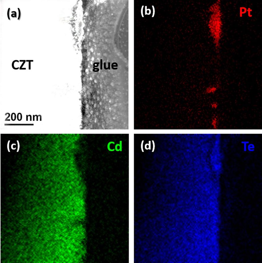
www.nature.com/scientificreports/
to reduce the off-stoichiometry7. Before platinum deposition, surfaces were lapped by means of abrasive paper
with particle size of 8 and 5 μm and then polished with 3 and 1 μm diamond powders. In order to minimize
surface oxidation, metal contacts were deposited onto the sample surface immediately after the polishing step.
Gold was deposited by using electroless deposition using alcoholic s olutions8 whereas platinum was deposited
by using the technique described below. In order to verify the mechanical resistance of contacts, we performed
the tape test using a standard tape (model 3M 600) and following the ISO 2409 procedure which allows to com-
pare results from different deposition techniques9,10. Lastly, we performed the photolithography of the samples
by etching the metal contact with a Br2 solution.
Structural characterization. Cross-sectional Transmission Electron Microscopy (TEM) and Energy Dis-
persive X-ray Spectroscopy (EDX) have been performed in order to investigate the structural and material prop-
erties of the Pt layer. EDX maps have been obtained in Scanning-TEM (STEM) mode using high-angle annular
dark-field (HAADF) detector.
For current–voltage characterization and spectroscopic characterization, a 5.5 × 5.5 × 2 mm3 sample (sample
AA) and a 6 × 5.7 × 1.1 mm3 sample (sample PP) were cut from the same REDLEN detector. A full-area cathode
m2 anode (pixel), this last surrounded by a guard ring, were patterned by means of photolithography
and a 4 × 4 m
on the opposite faces of both samples (see Supplementary Fig. S1 online). Current/voltage characteristics were
performed with a Keithley 2410 sourcemeter and a Keithley 6485 picoammeter.
X‑ray and gamma ray measurements. Uncollimated X-ray and gamma ray calibration sources
(gamma-ray lines: 241Am, 59.5 and 26.3 keV; 57Co, 122.1 and 136.5 keV) were used to characterize the spectro-
scopic performance of the detectors. The 14 keV gamma line of the 57Co source is shielded by the source holder.
Tungsten K X-ray fluorescent lines (Kα1 = 59.3 keV, Kα2 = 58.0 keV, Kβ1 = 67.2 keV, Kβ3 = 66.9 keV) and Np L X-ray
lines are also emitted by 57Co and 241Am sources, respectively. All detectors were irradiated through the cathode
side. The detectors signals were amplified by using a resistive feedback ac-coupled charge sensitive preamplifier
CSP (A250, Amptek, USA) with a nominal equivalent noise charge (ENC) of 100 electrons. Energy X-ray and
gamma ray spectra were obtained with a standard analog pulse processing electronics: shaping amplifier (672,
ORTEC, USA) with a shaping time constant of 1 μs and multichannel analyser (MCA-8000A, Amptek, USA).
Further details of spectroscopic set-up are reported in previous w orks11.
Laser induced transient current measurements. As a further investigation, carrier mobility and life-
time measurements were obtained by means of Laser Induced Transient Current Technique (LI-TCT)12 on an
additional set of samples based on CZT from REDLEN and from IMEM-CNR, on which Pt contacts were depos-
ited on the opposite surfaces.
Two samples with platinum contacts were manufactured for laser-induced transient current characterization.
The first sample (A) was cut from a crystal grown at IMEM by Boron Encapsulated Vertical Bridgman technique,
and had dimensions of 4 × 4 × 1 mm3. A central 2 × 2 m m2 pixel surrounded by the guard ring was realized on the
cathode. The second sample (B) was obtained by a REDLEN detector and had dimensions of 6 × 6 × 1.1 m m3. As
anode contact a central 4 × 4 m m2 pixel surrounded by the guard ring was realized (see Supplementary Fig. S2
online). In order to prevent undesired interaction with light during the measurements, samples were completely
encapsulated in epoxy glue except for a narrow hole through which the sample was irradiated by means of an
optical fiber. The typical applied bias voltage varied greatly depending on the type of investigated carrier because
of the difference between electron and hole µτ product in CZT: from few to tens of volts in the former case; from
tens to hundreds of volts in the latter.
Making use of a Nd:YAG Polaris II laser system, samples have been optically excited impinging an area of
about few hundreds of μm in diameter, at the center of the cathode. 532 nm pulses (second harmonic of Nd:YAG
laser) are 10 ns long, and with maximum repetition rate of 20 Hz. Light is simultaneously brought on the sample
and on a fast photodiode that acts as pulse trigger by means of two optical fibers of the same length. The pulse
energy released on the CZT is the same for all the acquired current transients. Low power laser pulse has been
used in order to prevent transient distortions due to high number of photogenerated charges. To reduce noise
contribution and little fluctuation of photogenerated charge, a few thousands of current pulses have been aver-
aged thanks to the trigger system.
The output signals, coming from the pixel, have been amplified by a home-made amplifier (up to 400 times)
with bandwidth of 80 MHz. Bias voltage has been supplied by a Keithley 2410 High Voltage Source Measure
Unit. The current transients have been acquired by a DS8202 Owon digital oscilloscope with 1 GHz bandwidth
and saved on a computer by means of Matlab software.
By using an excitation energy above the energy gap and changing the sign of bias, LI-TCT measurements
allow to study transport features for one kind of charge carrier at a time as a consequence of the Ramo-Shockley
theorem13. The attenuation length of a tenth of a μm at 532 nm, as estimated by the absorption coefficient of
Cd0.9Zn0.1Te reported in14, ensures photon absorption takes place mainly at a depth, underneath the illuminated
contact, that is only about 0.02% of the active thickness of detectors. It is then correct to assume the main amount
of charges travelling inside the detector are generated immediately under the illuminated contact.
The electrodes are thin enough to ensure that the majority of the incoming photons reaches the active region
of the detectors. The lateral surface of samples has been shielded to prevent absorption of reflected/diffused
light; this is important to prevent unwanted generation of signal at depths other than that just below the metal
contact where the laser is focused.
Scientific Reports | (2020) 10:13762 | https://doi.org/10.1038/s41598-020-70801-9 2
Vol:.(1234567890)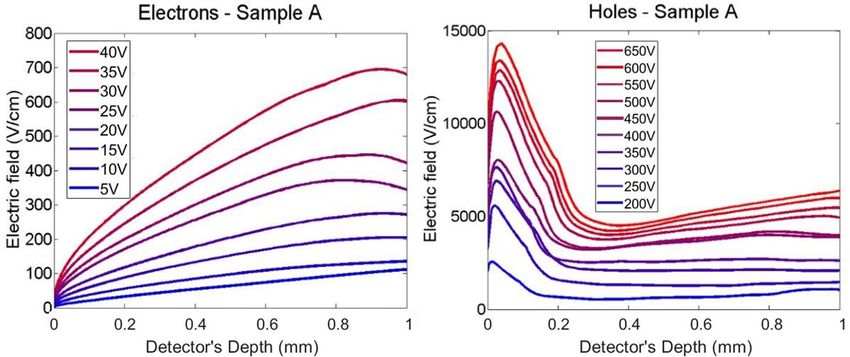
www.nature.com/scientificreports/
Figure 1. Platinum contact obtained by standard electroless procedure and the tape status after the tape test
(a); Platinum contact obtained by MeOH/DMF electroless procedure, and the tape status after the tape test (b);
Schematic representation of the Pt deposition setup (c).
Experiments here reported require a low repetition rate to ensure the laser does not affect the polarization
of material. Repetition rate and beam energy are carefully calibrated to ensure a negligible variation of space
charge inside the samples.
LI-TCT method, used in this work and described in12 or more in detail in15, could be useful to investigate
space charge distribution inside the volume of detectors even after high flux damaging. For a comparison with
other approaches, see also16–18.
Contact deposition. Firstly, Pt contacts were realized using standard electroless procedures1,2. The electro-
less solutions were prepared with platinum chloride (PtCl4) as precursor which can react both with Cd and Te2:
PtCl62− + Cd(s) ⇒ PtCl42− + 2Cl − + Cd 2+ ≫ �E = +1.09V
PtCl42− + Cd(s) ⇒ Pt(s) + 4Cl − + Cd 2+ ≫ �E = +1.16V
2PtCl62− + Te(s) ⇒ 2PtCl42− + 4Cl − + Te4+ ≫ �E = +0.11V
2PtCl42− + Te(s) ⇒ Pt(s) + 8Cl − + Te4+ ≫ �E = +0.19V
The different chemical potentials indicate that platinum reacts mainly with cadmium, thus transferring C d2+
ions and leaving a Te-rich layer on CZT on which metal Pt atoms p recipitate8,19. Thus far, platinum deposition
was not an easy and always successful process. Literature reports platinum electroless deposition from water or
methanol solutions at room temperature1,2. However, platinum layers deposited in such conditions (2% of PtCl4
in water solution at 25 °C) are not uniform and consist of islands with various extent and thickness, even if salt
concentration and deposition time are varied. These contacts also show poor mechanical stability and cannot
withstand the tape test (Fig. 1a). In fact, adhesion is still one of the major issues for contacts on CZT, the situation
being worsened by the instability of CZT at high temperature that cause the impossibility of annealing contacts.
By using a 4% (w/w) platinum chloride solution in 1:1 methanol/dimethylformamide (DMF), an optimal
deposition of Pt film can be achieved. Heating the solution up to 60–70 °C with mechanical stirring significantly
speeds up the dissolution of platinum salt. The resulting electroless solution can be stored in an amber vial at 4 °C
for several weeks. DMF has been previously investigated as a solvent for the synthesis of s emiconducting20 and
metal nanoparticles (NPs)21 mainly because of the high dielectric constant and coordinating ability. DMF can
reduce metal salts and form NPs or films depending on the synthetic condition (mainly solution supersaturation
and ligand complexation), even though the room temperature reaction, without reducing agents, can be very
slow22. In the proposed method, samples were placed on a hotplate heated up to 100 °C, then 50 μL of the cooled
(4 °C) solution was drop-casted on the samples and illuminated with a 300 W halogen lamp for 5 min (Fig. 1c).
This triggers the electroless deposition of the platinum layer. The drop-casting procedure can be repeated several
Scientific Reports | (2020) 10:13762 | https://doi.org/10.1038/s41598-020-70801-9 3
Vol.:(0123456789)
www.nature.com/scientificreports/
Figure 2. Cross section TEM–EDX analysis for the Pt contact obtained in water, STEM-HAADF image (a) and
corresponding EDX maps for Pt (b), Cd (c), Te (d).
times to tailor the Pt layer thickness. We found that repeating 3 times ensures a uniform, 60 nm thick, film
deposition. Finally, samples were cooled down and rinsed with deionized water.
The final metal layer appears homogeneous, shiny and smooth (Fig. 1b). After this procedure, Pt contacts
withstand at last the tape test.
Results
TEM analyses. Figure 2 shows the cross section TEM–EDX analysis for the Pt contact obtained in water, the
STEM-HAADF image (a) and corresponding EDX maps for Pt (b), Cd (c), Te (d). Images reveal that the contact
is formed by Pt islands and is, thus, very inhomogeneous.
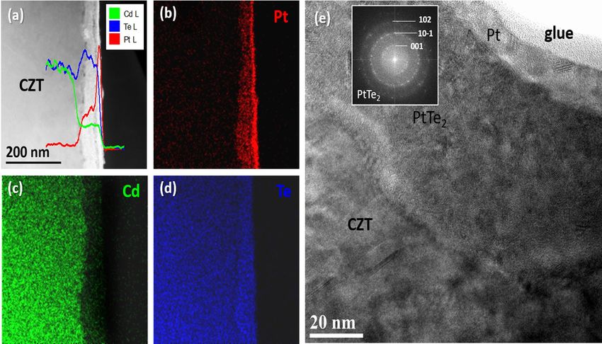
Figure 3a shows a STEM-HAADF image of the MeOH/DMF Pt contact and the relative composition profile
of Pt, Cd and Te. EDX maps of the same region are reported in Fig. 3b–d. The thickness of the deposited contact
layer is about 60 nm and is continuous in respect to that obtained by deposition in water. As revealed by the
composition profile, the contact layer is composed of a top 20 nm-thick Pt layer, followed by a region of ∽ 40 nm
characterized by a mixture of Pt and Te. In correspondence with this layer, a Cd depleted region can be noticed
eposition19,23. The extent of the Cd depletion has been previously associated to the
which is typical of electroless d
mechanical stability of the contact8. In the present case, this does not hold, because a Pt-Te compound is formed.
In order to identify the phase of the PtTe layer, High Resolution TEM was employed in this region (Fig. 3e).
The presence of rings in the Fast Fourier Transform pattern confirms the polycrystallinity of the contact layer
and their position is consistent with that of a P tTe2 alloy. This explains also the increase of Te contents in respect
to the bulk material (Fig. 3a). PtTe2 is known to be metallic alloy.
Scientific Reports | (2020) 10:13762 | https://doi.org/10.1038/s41598-020-70801-9 4
Vol:.(1234567890)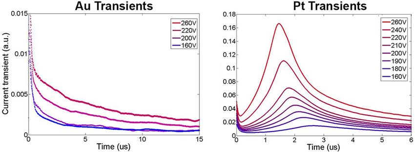
www.nature.com/scientificreports/
Figure 3. (a) Cross section STEM-HAADF image with the superimposed composition profile of Pt, Cd and
Te. (b–d) Pt, Cd and Te EDX maps of the same region. (e) High Resolution TEM of the MeOH/DMF Pt contact
with the Fast Fourier transform of the PtTe2 layer in the inset.
Figure 4. JV comparison for AA and PP samples. In the small pane are shown the JV between ± 2 V/mm.
Electrical properties. The current- voltage characteristics of the Pt and Au detectors are shown in Fig. 4.
At low voltages (the inset of Fig. 4), both samples highlight a “S” shape curve, typical of metal–semiconductor–
metal (MSM) contacts with two back-to-back Schottky b arriers24–26. In this region, the current is dominated by
the bulk resistivity and the contact resistance. The Pt detector shows a lower current and a better ohmic contact
than those of Au detector, confirming the results reported in27. At high voltages, an exponential behaviour is
observed: the crystal is fully depleted and the transport mechanism is governed by the interfacial layer–thermi-
onic-diffusion (ITD) model4. This model foresees the existence of a very thin insulating layer, probably formed
during the contact deposition, between the contact and the semiconductor material. This oxide layer can be due
to the oxidation of Te-rich layer of CZT surface before Pt deposition28. ITD model incorporates the thermionic-
diffusion theory across the Schottky barrier between the metal on the lightly doped semiconductor with the tun-
neling transport mechanism across the thin oxide layer29. According to the ITD model, the CZT detector with
negative voltage at the cathode can be treated as a metal–semiconductor system consisting of a reversed-biased
Scientific Reports | (2020) 10:13762 | https://doi.org/10.1038/s41598-020-70801-9 5
Vol.:(0123456789)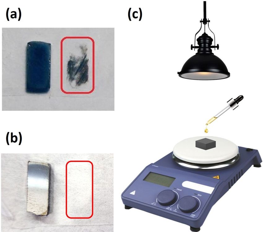
www.nature.com/scientificreports/
q
Figure 5. Arrhenius plots log J/T 2 versus kT for the Pt detector.
q
Figure 6. Arrhenius plots log J/T 2 versus kT for the Au detector.
Schottky barrier at the cathode4. In this case the reverse current J is due to the majority carriers of the CZT crys-
tal. For n-type CZT and in the voltage range where the thermionic-emission dominates J can be expressed a s30:
φ VC 2
− V B0
J = θn A∗n T 2 e TH e VTH (1)
where V is the reverse voltage on the CZT/Metal junction, VTH = kT/q is the thermal voltage, A∗n = 120 m∗e /me
is the is the electron effective Richardson constant, where m∗e and me are the effective and free electron mass,
respectively. φB0 is the energy barrier height under thermal equilibrium conditions, θn , with 0 < θn < 1, is the
electron transmission coefficient across the interfacial layer and C2 = ε +2qεi2 δD where εi and δ are the permittivity
i s
and thickness of the interfacial layer, and Ds is the density of surface states per unit energy and area. For p-type
CZT material, Equation holds by replacing θn and A∗n with the hole transmission coefficient θh and the hole effec-
tive Richardson constant A∗h = 120m∗h /me , where m∗h is the effective hole mass. For CdTe crystals, m∗e = 0.1 and
m∗h = 0.726. By assuming n-type CZT material and following the procedure used in30 we estimated φB0, θn and
C2 for both samples, by measuring the reverse J-V curves at different temperatures (− 5 °C; 25 °C). In particular,
C2 was obtained by fitting (Eq. 1) the reverse J–V curves in the high voltage region at different temperatures. In
the voltage range where the coefficient C2 is independent of temperature the thermoionic-emission dominates.
q
The values of φB0 and θn have been extracted from the Arrhenius plots log J/T 2 versus kT , as shown in Figs. 5
and 6 for the Pt and Au detectors at V = − 150 V, respectively. The values of the parameters are shown in Table 1.
Scientific Reports | (2020) 10:13762 | https://doi.org/10.1038/s41598-020-70801-9 6
Vol:.(1234567890)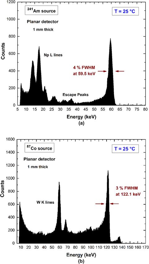
www.nature.com/scientificreports/
φB0 (eV) θn C2
Pt 0.78 ± 0.03 0.05 ± 0.01 1.56 × 10⁻⁴
Au 0.75 ± 0.01 0.013 ± 0.005 5.62 × 10⁻⁵
Table 1. Values of φB0, θn and C2 parameters extracted from the ITD model for the Pt and Au CZT detectors.
Figure 7. (a) Measured 241Am and (b) 57Co spectra with the Pt-CZT planar detectors.
Both samples show similar values of the barrier height and the transmission coefficient, in agreement with the
literature4,30,31. While, the coefficient C2 of the Pt contact is larger than the Au one. This explains the prompt
increasing of the current of the Pt detector at voltages above 100 V/mm. C2 depends on the product δDs , i.e. on
the thickness of the oxide layer and the density of surface states at the CZT/metal interface. The transmission
coefficient is related to the thickness of the oxide layer ( θn ∝ e−δ)29 and being the θn values of the Pt and Au
contacts comparable, we can conclude that the higher leakage current in the Pt detector is due to the lower density
of interface states of the Pt contact.
Spectroscopic performance. The spectroscopic capabilities of the detectors were investigated. The meas-
ured 241Am and 57Co energy spectra at low rate conditions (< 300 counts/s) are shown in Fig. 7. The detectors
were biased with an electric field of 1,500 V/cm at room temperature. The spectroscopic performances are com-
parable to Au-detectors, as previously presented in our works32. The effects of hole trapping (peak asymmetry
and tailing) are clearly visible in the measured spectra, mainly in the 57Co energy spectrum. As widely docu-
mented in the literature33,34, both electrons and holes contribute to the formation of the charge pulses in planar
detectors. In particular, photon interactions near the anode electrode create charge pulses with an increased hole
Scientific Reports | (2020) 10:13762 | https://doi.org/10.1038/s41598-020-70801-9 7
Vol.:(0123456789)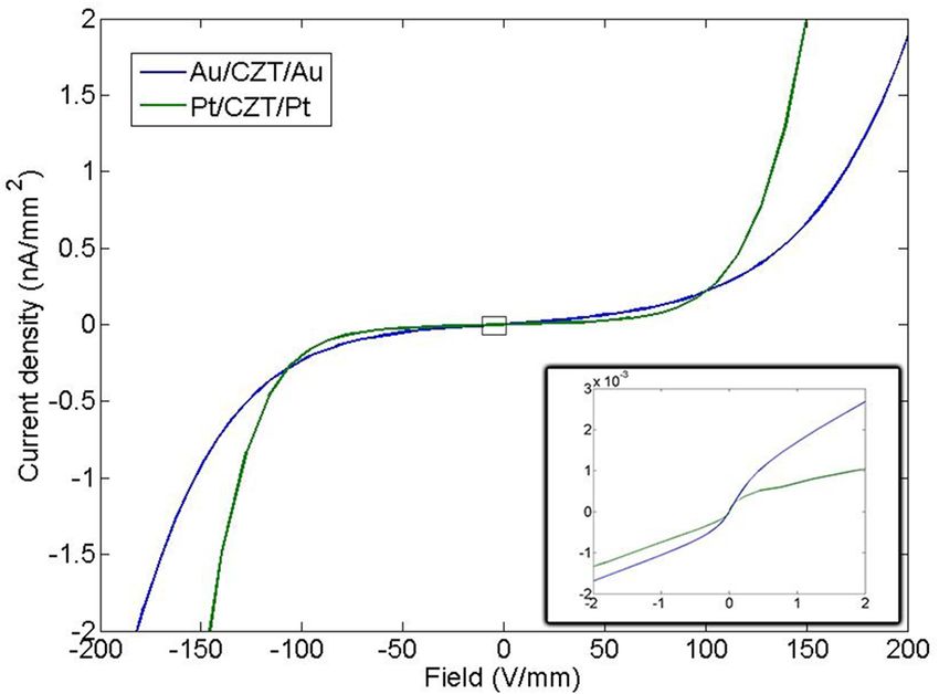
www.nature.com/scientificreports/
Figure 8. Typical current transients related to hole signal for Au (left) and Pt (right) contacts at different
applied bias voltage.
Figure 9. Electric field profiles for electrons (left) and for holes (right) of sample A at different bias voltage.
contribute and, therefore, characterized by higher hole trapping effects. In our case, this mainly happens for the
122 keV photons of the 57Co source that are characterized by a mean free path of 1.9 mm on CZT material35.
Generally, these effects can be mitigated by using unipolar detectors33,34, which charge pulses are mainly sensitive
to the electrons. These detectors are typically realized with pixel or strip structures on the anode electrode36,37
and by using bi-parametric correction techniques38,39.
Laser induced transient current technique. LI-TCT demonstrated to be a powerful method to meas-
ure carrier transport p roperties15,40–42. However, in the papers published up to now, only electron transport prop-
erties were determined. This is because, the common gold contacts show a weak and noisy hole signal. On the
other hand, we found out that samples with platinum contacts revealed a detectable hole signal. In Fig. 8, typical
current transients for Pt and Au contacts, related to hole signal, are reported as example.
Figures 9 and 10 report the calculated electric field profiles of the two samples for both electrons and holes,
as extracted analysing electrical transients as reported in15. It is advisable to underline that the calculated electric
field profiles are those experienced by the charge carrier during the motion along the device and, as a consequence
of different biases used for electrons and holes, a comparison between results for charge carriers of opposite
sign is not so easy to do. In addition, the reconstruction of the electric field suffers from artefacts in proximity
of the electrodes, especially near the illuminated one (on the left in Figs. 9 and 10). Since the profile of the field
has been deduced from the current transient curves, the electric field near this electrode could be affected by the
effect of a non-instantaneous light excitation that is not completely removed from the laser pulse deconvolution.
Further, we cannot exclude the presence of space charge related to the interfacial defectiveness of the material.
The electric field calculated from LI-TCT transients for electrons shows in both samples a nearly linear
increase that could be ascribed to an almost uniform negative space charge inside the sample. The higher slope
in the sample A suggests a higher density of such space charge. Trapping of negative charge is realistic because
the carriers travelling along the device are electrons.
Scientific Reports | (2020) 10:13762 | https://doi.org/10.1038/s41598-020-70801-9 8
Vol:.(1234567890)www.nature.com/scientificreports/
Figure 10. Electric field profiles for electrons (left) and for holes (right) of sample B at different bias voltage.
Sample Electrons mobility µe (cm2/Vs) Electrons life-time τe(μs) Holes mobility µh (cm2/Vs) Holes life-time τh(μs)
A 1,408 0.65 36 1.97
B 1,032 0.65 28 >5
Table 2. Carriers mobility and lifetime extracted from LI-TCT measurements.
Electric field reconstructed from hole transients exhibits a strong decreasing slope in the first 100 ÷ 200
microns close to the illuminated electrode. This phenomenon is stronger in sample A and it can newly traced
back to trapping of negative charges localized mainly under the anode. When the distance from the cathode
is greater than about 100 ÷ 200 μm from the illuminated electrode, sample A shows an almost uniform trend
for the electric field whereas the trend in the sample B is growing up to about 600 μs it begins to decrease. The
difference between sample A and sample B could be justified taking into account the residual negative charge
trapping, already proved by electron measurements, that is now compensated by holes trapping along the thick-
ness of detectors. The effect of compensation is less effective in sample A due to both a higher negative space
charge density and a higher hole mean free path with respect sample B, in which a relative maximum of electric
field is reached at about 600 μs in depth.
Mean free path for electrons and holes can be calculated by the transport parameters obtained for both car-
riers and reported in Table 2. All results are in agreement with literature values reported for CZT15,43,44.
The values of hole mobility in the two samples are similar as expected. The model is unable to provide the
holes lifetime for sample B since times of flight is shorter than lifetime for all the investigated applied voltages.
Because of this, we have not enough data to reconstruct the carrier trapping process. The only way to increase
time of flight is to decrease the bias voltage. However, measuring transients with voltages lower than 100 V is
not trivial since the signal becomes comparable with noise. We can only assume that the lifetime is greater than
the highest time of flight (5 μs for sample B). Sample A shows a significant lower hole lifetime: such difference
can be easily ascribed to the different growth technologies.
Discussion
We realized Pt Schottky contacts deposited on CdZnTe with a novel procedure based on the electroless technique.
The use of methanol/DMF as solvent allows the formation of homogeneous and mechanically stable contacts,
able to withstand a standard tape test.
TEM analysis showed that a continuous Pt layer is formed in contrast to water deposition. Below the Pt layer,
a PtTe2 alloy is formed. This is a different situation with respect to gold electroless deposition, where a Te layer
is formed as a consequence of Cd depletion p rocess8,19.
Electrical characterisation showed that the Pt contact in the ± 2 V/mm range has lower current density than
that of Au contact. Probably, this is due the higher energy barrier of platinum contacts (see Table 1). At high
voltages, the current density of platinum contacts increases and exceeds that of gold contacts. According to the
ITD model, this behaviour can be explained by the lower density of states at the metal semiconductor interface,
probably related to the formation of the PtTe2 alloy.
Energy resolution of γ-ray spectra for detectors realized with Pt contacts is comparable with those realized
using gold contacts so that platinum is a good contact for spectroscopic applications.
Thanks to platinum contacts, for the first time we were able to measure hole mobility and lifetime by means
of LI-TCT, while, with gold contacts, that was not possible. This also means that Pt contacts actually ease the
hole collection with respect to gold contacts. The admirable hole collection efficiency of Pt/CZT contacts can be
Scientific Reports | (2020) 10:13762 | https://doi.org/10.1038/s41598-020-70801-9 9
Vol.:(0123456789)www.nature.com/scientificreports/
exploited for detectors working under high flux conditions, where the removal of low mobility holes is generally
an issue45.
Further studies are ongoing in order to deposit a thicker electroless Pt layer without the need of sample
heating. Room-temperature deposition would ease the photolithographic process and open the possibility to
pattern fine-pitch electrodes.
Received: 20 April 2020; Accepted: 3 July 2020
References
1. Zheng, Q. et al. Comparison of radiation detector performance for different metal contacts on CdZnTe deposited by electroless
deposition method. Cryst. Res. Technol. 46, 1131–1136 (2011).
2. Zheng, Q. et al. Electroless deposition of Au, Pt, or Ru metallic layers on CdZnTe. Thin Solid Films 525, 56–63 (2012).
3. Raulo, A. et al. Ion beam (RBS) and XRF analysis of metal contacts deposited on CdZnTe and CdTe crystals. IEEE Trans. Nucl.
Sci. 58(4 PART 2), 1964–1971 (2011).
4. Bolotnikov, A. E. et al. Properties of Pt Schottky type contacts on high-resistivity CdZnTe detectors. Nucl. Instrum. Methods Phys.
Res. A 482(1–2), 395–407 (2002).
5. Zha, M. et al. Full encapsulated CdZnTe crystals by the vertical Bridgman method. J. Cryst. Growth 310(7–9), 2072–2075 (2008).
6. Zappettini, A. et al. New process for synthesizing high-purity stoichiometric cadmium telluride. J. Cryst. Growth. 214, 14–18
(2000).
7. Zha, M. et al. Heat treatment in semi-closed ampoule for obtaining stoichiometrically controlled cadmium telluride. J. Cryst.
Growth 237, 1720–1725 (2002).
8. Benassi, G. et al. Strong mechanical adhesion of gold electroless contacts on CdZnTe deposited by alcoholic solutions. J. Instrum.
12(2), P02018 (2017).
9. Shwartz, G. C. Handbook of semiconductor interconnection technology (CRC Press, Boca Raton, 2006).
10. A. IPC-TM-650 Test Methods Manual.
11. Abbene, L. et al. X-ray response of CdZnTe detectors grown by the vertical Bridgman technique: Energy, temperature and high
flux effects. Nucl. Instrum. Methods Phys. Res. Sect. A Accel. Spectrom. Detect. Assoc. Equip. 835, 1–2 (2016).
12. Santi, A. et al. An original method to evaluate the transport parameters and reconstruct the electric field in solid-state photodetec-
tors. Appl. Phys. Lett. 104(19), 0–4 (2014).
13. Ramo, S. Currents induced by electron motion. Proc IRE 27(9), 584–585 (1939).
14. Yao, H. W., Erickson, J. C., Barber, H. B., James, R. B. & Hermon, H. Optical properties of Cd0.9Zn0.1 Te studied by variable angle
spectroscopic ellipsometry between 0.75 and 6.24 eV. J. Electron. Mater. 28(6), 760–765 (1999).
15. Yao, H. W., Erickson, J. C., Barber, H. B., James, R. B. & Hermon, H. Electric field reconstruction and transport parameter evalu-
ation in CZT X-ray detectors. IEEE Trans. Nucl. Sci. 64(10), 2706–2712 (2017).
16. Eremin, V., Strokan, N., Verbitskaya, E. & Li, Z. Development of transient current and charge techniques for the measurement of
effective net concentration of ionized charges (Neff) in the space charge region of p-n junction detectors. Nucl. Instrum. Methods
Phys. Res. Sect. A Accel. Spectrom. Detect. Assoc. Equip. 372(3), 388–398 (1996).
17. Kraner, H. W., Li, Z. & Fretwurst, E. The use of the signal current pulse shape to study the internal electric field profile and trap-
ping effects in neutron damaged silicon detectors. Nucl. Instrum. Methods Phys. Res. Sect. A Accel. Spectrom. Detect. Assoc. Equip.
326(1–2), 350–356 (1993).
18. Kalliokoski, M. et al. Charge collection measurements of CdTe detectors using IBIC imaging method. In 2018 IEEE Nuclear Science
Symposium and Medical Imaging Conference Proceedings (NSS/MIC) (2018).
19. Bell, S. J. et al. A multi-technique characterization of electroless gold contacts on single crystal CdZnTe radiation detectors. J. Phys.
D Appl. Phys. 46(45), 455502 (2013).
20. Villani, M. et al. Extended functionality of ZnO nanotetrapods by solution-based coupling with CdS nanoparticles. J. Mater. Chem.
22(12), 5694–5699 (2012).
21. Nagata, T. & Obora, Y. N,N-dimethylformamide-protected single-sized metal nanoparticles and their use as catalysts for organic
transformations. ACS Omega. 5(1), 98–103 (2020).
22. Pastorizo-Santos, I. & Liz-Marzán, L. M. N,N-dimethylformamide as a reaction medium for metal nanoparticle synthesis. Adv.
Funct. Mater. 19(5), 679–688 (2009).
23. Roumié, M. et al. Ion beam analysis of CdTe nuclear detector contact grown by electroless process. Nucl. Instrum. Methods. Phys.
Res. Sect. B Beam Interact. Mater. Atom 240(1–2), 386–390 (2005).
24. Bell, S. J. et al. Characterization of the metal-semiconductor interface of gold contacts on CdZnTe formed by electroless deposition.
J. Phys. D Appl. Phys. 48(27), 275304 (2015).
25. Marchini, L. et al. Study of surface treatment effects on the metal-CdZnTe interface. IEEE Trans. Nucl. Sci. 56(4), 1823–1826 (2009).
26. Prokesch, M. & Szeles, C. Accurate measurement of electrical bulk resistivity and surface leakage of CdZnTe radiation detector
crystals. J. Appl. Phys. 100(1), 014503 (2006).
27. Lee, S. H. et al. Comparison on the performance of a gamma-ray spectrometer with the variation of Pt(Au)/CdZnTe/Pt(Au)
interface. J. Cryst. Growth 214, 1111–1115 (2000).
28. Bolotnikov, A. E. et al. Effects of bulk and surface conductivity on the performance of CdZnTe pixel detectors. IEEE Trans. Nucl.
Sci. 49(4), 1941–1949 (2002).
29. Wu, C.-Y. «Interfacial layer-thermionic-diffusion theory for the Schottky barrier diode. J. Appl. Phys. 53(8), 5947–5950 (1982).
30. Turturici, A. A. et al. Electrical properties of Au/CdZnTe/Au detectors grown by the boron oxide encapsulated Vertical Bridgman
technique. Nucl. Instrum. Methods Phys. Res. Sect. A Accel. Spectrom. Detect. Assoc. Equip. 830, 243–250 (2016).
31. Bell, S. J. et al. Comparison of the surfaces and interfaces formed for sputter and electroless deposited gold contacts on CdZnTe.
Appl. Surf. Sci. 427, 1257–1270 (2018).
32. Abbene, L. et al. Development of new CdZnTe detectors for room-temperature high-flux radiation measurements. J. Synchrotron
Radiat. 24(2), 429–438 (2017).
33. He, Z. Review of the Shockley-Ramo theorem and its application in semiconductor gamma-ray detectors. Nucl. Instrum. Methods
Phys. Res. Sect. A Accel. Spectrom. Detect. Assoc. Equip. 463(1–2), 250–267 (2001).
34. del Sordo, S. et al. Progress in the development of CdTe and CdZnTe semiconductor radiation detectors for astrophysical and
medical applications. Sensors 9, 3491–3526 (2009).
35. Boone, J. M. & Chavez, A. E. Comparison of x-ray cross sections for diagnostic and therapeutic medical physics. Med. Phys. 23(12),
1997–2005 (1996).
36. Barrett, H. H., Eskin, J. D. & Barber, H. B. Charge transport in arrays of semiconductor gamma-ray detectors. Phys. Rev. Lett. 75(1),
156–159 (1995).
Scientific Reports | (2020) 10:13762 | https://doi.org/10.1038/s41598-020-70801-9 10
Vol:.(1234567890)www.nature.com/scientificreports/
37. Del Sordo, S. et al. Spectroscopic performances of 16 x 16 pixel CZT imaging hard-X-ray detectors. Nuovo Cimento Soc. Ital. Fis.,
B 119(3), 257–270 (2004).
38. Abbene, L. & Gerardi, G. Performance enhancements of compound semiconductor radiation detectors using digital pulse process-
ing techniques. Nucl. Instrum. Methods Phys. Res. Sect. A Accel. Spectrom. Detect. Assoc. Equip. 654(1), 340–348 (2011).
39. Jones, L. & Woollam, P. Resolution improvement in CdTe gamma detectors using pulse-shape discrimination. Nucl. Instrum.
Methods 124(2), 591–595 (1975).
40. Belas, E., Praus, P., James, R. B., Grill, R. & Uxa, Š. Determination of electric-field profile in CdTe and CdZnTe detectors using
transient-current technique. IEEE Trans. Nucl. Sci. 59(5), 2402–2408 (2012).
41. Bettelli, M., Santi, A., Pavesi, M., Calestani, D. & Zappettini, A. Overcoming the planar contact geometry limitation for the meas-
urement of transport properties and electric field distribution in X- and gamma ray detectors. Nucl. Instrum. Methods Phys. Res.
Sect. A Accel. Spectrom. Detect. Assoc. Equip. 908, 411–415 (2018).
42. Vasylchenko, I., Grill, R., Belas, E., Praus, P. & Musiienko, A. Charge sharing in (CdZn)te pixel detector characterized by laser-
induced transient currents. Sensors 20(1), 85 (2020).
43. Fink, J., Krüger, H., Lodomez, P. & Wermes, N. Characterization of charge collection in CdTe and CZT using the transient current
technique. Nucl. Instrum. Methods Phys. Res. Sect. A Accel. Spectrom. Detect. Assoc. Equip. 560(2), 435–443 (2006).
44. Jung, M., Morel, J., Fougères, P., Hage-Ali, M. & Siffert, P. New method for evaluation of transport properties in CdTe and CZT
detectors. Nucl. Instrum. Methods Phys. Res. Sect. A Accel. Spectrom. Detect. Assoc. Equip. 428(1), 45–57 (1999).
45. Bale, D. S. & Szeles, C. Nature of polarization in wide-bandgap semiconductor detectors under high-flux irradiation: Application
to semi-insulating Cd1-x Znx Te. Phys. Rev. B Condens. Matter Mater. Phys. 77(3), 035205 (2008).
Author contributions
M.B. and M.V. conceived the deposition technique. A.Z. planned the experiments. M.B., N.S.A., S.Z. and M.V.
contributed to samples preparation. M.B., N.S.A. and L.N. performed the structural characterization. L.A. and
F.P. performed the electrical characterization and tested the spectroscopic performance of samples. M.B., A.S.
and M.P. carried out the LI-TCT experiments. A.Z. supervised the project. M.B. and N.S.A. wrote the manuscript
with input from all authors. All authors discussed the results and reviewed the manuscript.
Competing interests
The authors declare no competing interests.
Additional information
Supplementary information is available for this paper at https://doi.org/10.1038/s41598-020-70801-9.
Correspondence and requests for materials should be addressed to N.S.A.
Reprints and permissions information is available at www.nature.com/reprints.
Publisher’s note Springer Nature remains neutral with regard to jurisdictional claims in published maps and
institutional affiliations.
Open Access This article is licensed under a Creative Commons Attribution 4.0 International
License, which permits use, sharing, adaptation, distribution and reproduction in any medium or
format, as long as you give appropriate credit to the original author(s) and the source, provide a link to the
Creative Commons licence, and indicate if changes were made. The images or other third party material in this
article are included in the article’s Creative Commons licence, unless indicated otherwise in a credit line to the
material. If material is not included in the article’s Creative Commons licence and your intended use is not
permitted by statutory regulation or exceeds the permitted use, you will need to obtain permission directly from
the copyright holder. To view a copy of this licence, visit http://creativecommons.org/licenses/by/4.0/.
© The Author(s) 2020
Scientific Reports | (2020) 10:13762 | https://doi.org/10.1038/s41598-020-70801-9 11
Vol.:(0123456789)You can also read