Tunable Multilevel Data Storage Bioresistive Random Access Memory Device Based on Egg Albumen and Carbon Nanotubes - MDPI
←
→
Page content transcription
If your browser does not render page correctly, please read the page content below
nanomaterials

Article
Tunable Multilevel Data Storage Bioresistive Random Access
Memory Device Based on Egg Albumen and Carbon Nanotubes
Lu Wang *, Tianyu Yang and Dianzhong Wen

                                          HLJ Province Key Laboratory of Senior-Education for Electronic Engineering, School of Electronic Engineering,
                                          Heilongjiang University, Harbin 150080, China; 2201633@s.hlju.edu.cn (T.Y.); wendianzhong@hlju.edu.cn (D.W.)
                                          * Correspondence: wanglu@hlju.edu.cn; Tel.: +86-188-4502-5666

                                          Abstract: In this paper, a tuneable multilevel data storage bioresistive memory device is prepared
                                          from a composite of multiwalled carbon nanotubes (MWCNTs) and egg albumen (EA). By changing
                                          the concentration of MWCNTs incorporated into the egg albumen film, the switching current ratio of
                                          aluminium/egg albumen:multiwalled carbon nanotubes/indium tin oxide (Al/EA:MWCNT/ITO)
                                          for resistive random access memory increases as the concentration of MWCNTs decreases. The device
                                          can achieve continuous bipolar switching that is repeated 100 times per cell with stable resistance for
                                          104 s and a clear storage window under 2.5 × 10⁴ continuous pulses. Changing the current limit of
                                          the device to obtain low-state resistance values of different states achieves multivalue storage. The
                                          mechanism of conduction can be explained by the oxygen vacancies and the smaller number of iron
                                          atoms that are working together to form and fracture conductive filaments. The device is nonvolatile
                                          and stable for use in rewritable memory due to the adjustable switch ratio, adjustable voltage, and
                                nanometre size, and it can be integrated into circuits with different power consumption requirements.

                                          Therefore, it has broad application prospects in the fields of data storage and neural networks.
Citation: Wang, L.; Yang, T.; Wen, D.
Tunable Multilevel Data Storage           Keywords: egg albumen; carbon nanotubes; multilevel data storage; tuneable resistive random
Bioresistive Random Access Memory         access memories
Device Based on Egg Albumen and
Carbon Nanotubes. Nanomaterials
2021, 11, 2085. https://doi.org/
10.3390/nano11082085                      1. Introduction
                                                Because von Neumann theory makes the development of modern technology difficult,
Academic Editor:
                                          resistive random-access memories (RRAMs) with storage and computing properties have
Christophe Detavernier
                                          been candidate devices to solve this problem. RRAMs have a simple structure, low power
                                          consumption, high integration potential, and fast read and write speeds; they also have
Received: 16 July 2021
Accepted: 15 August 2021
                                          multivalue computing potential and are very compatible with complementary metal oxide
Published: 17 August 2021
                                          semiconductor (CMOS) technology [1]. At present, the research status of RRAM has been
                                          extended to many application technology fields because it can exhibit synaptic behaviour
Publisher’s Note: MDPI stays neutral
                                          such as short-term plasticity (STP), long-term plasticity (LTP), spike-time-dependent plas-
with regard to jurisdictional claims in
                                          ticity (STDP), paired-pulse facilitation (PPF), and paired-pulse depression (PPD) [2]. This
published maps and institutional affil-   technology can be applied to neural networks and artificial intelligence; the RRAM of the
iations.                                  crossbar array can store and calculate integrated memory; it can be used in chaotic circuits
                                          to form a confidentiality system [3]. RRAM made for biological applications can be applied
                                          to wearable devices [4]. The characteristics and advantages of RRAMs are closely related
                                          to the materials used for making the devices, so the choice of materials is vital. RRAMs
Copyright: © 2021 by the authors.
                                          made of inorganic materials are fragile, incompatible, and difficult to degrade, which leads
Licensee MDPI, Basel, Switzerland.
                                          to immense challenges [5]. Great progress has been made in the fabrication of functional
This article is an open access article
                                          electronic devices using organic biomaterials, and a new generation of environmentally
distributed under the terms and           friendly and biocompatible natural bioorganic materials as functional layers of RRAM
conditions of the Creative Commons        has attracted increasing attention. Natural bioorganic materials such as nanocellulose [6],
Attribution (CC BY) license (https://     DNA [7,8], protein, chitosan [9], and starch [10] have been used in the fabrication of RRAM.
creativecommons.org/licenses/by/                The biodegradability and bioabsorbability of protein-based biological RRAMs make
4.0/).                                    them applicable for bioimplantable medical devices. They are often used in flexible wear-

Nanomaterials 2021, 11, 2085. https://doi.org/10.3390/nano11082085                                    https://www.mdpi.com/journal/nanomaterials
Nanomaterials 2021, 11, 2085                                                                                             2 of 11

                               able electronic devices due to their light weight, stretchability, and foldability. Protein
                               is nonhazardous, nonpolluting, easy to obtain, and can be mass produced at low cost.
                               Protein-based RRAMs of silk fibroin [11], silkworm haemolymph [12], sericin [13], and egg
                               protein [14,15] have been proposed. As a natural biological material, egg white does not
                               require additional chemical extraction and purification processes, which reduces manufac-
                               turing costs and simplifies processing steps. In 2015, Chen fabricated Al/EA/ITO RRAMs
                               using egg white as the active layer and found that the devices have nonvolatile bipolar
                               switching characteristics [16]. Qu proposed a novel one-write-multiread RRAM based on
                               a protein film, forming an Ag/EA/ITO/polyethylene terephthalate (PET) structure [17].
                               Wang controlled the current switching ratio of Al/graphene oxide (GO)/EA/GO/ITO
                               devices using varying concentrations of GO [18]. Other studies have demonstrated that
                               RRAMs made from egg proteins are water soluble [19], can successfully simulate the
                               memory behaviour of biological synapses [20–22], can be flexibly transferred to many
                               unconventional substrates [23], and can realize the full memory logic block of the non-gate,
                               or-gate, and and-gate [24]. Egg proteins can also be made into gate dielectric layers of
                               organic field effect transistors and other transistors [25,26]. Therefore, egg protein RRAMs
                               are competitive as biological RRAMs and have very broad research prospects.
                                    The egg protein RRAMs in the literature have a switching ratio of 102 to 107 , and their
                               resistance switching characteristics vary greatly. Therefore, it is valuable to find a way to
                               reliably adjust the resistance switching characteristics of the device. The bipolar resistance
                               switching behaviour is the result of the formation and rupture of conductive filaments
                               caused by ion migration in the active layer of the egg protein RRAM. The concentration
                               of migrating ions in the active layer could be precisely controlled to affect the resistance
                               switching behaviour of the biological protein RRAM. The concentration of doping in the
                               active layer greatly affects the concentration of migrating ions. However, there is a lack of
                               relevant research on adjustment of the doping level to significantly change the resistance
                               switching characteristics of egg protein RRAMs.
                                    As nanoscale structures of carbon, carbon nanotubes have excellent electrical, me-
                               chanical, thermal, and hydrogen storage properties; [27] therefore, they are used in new
                               electronic sources [28], sensors [29], composite materials [30], stealth materials [31], and hy-
                               drogen storage materials [32]. The orientation, arrangement, and additional conditions of
                               the MWCNTs added to the source layer result in RRAMs with novel characteristics [33,34].
                               Liu used a conjugated polymer mixed with carbon nanotubes to form the active layer
                               of RRAM, which exhibits a switching behaviour of one write and many reads [35]. Kim
                               developed a carbon nanotube RRAM with basic dynamic logic, learning and memory
                               functions for biological synapses [36]. Molinari used a nanocomposite of polycaprolactone,
                               multiwalled carbon nanotubes, and fullerene C60 as a memristor layer to create a one-write-
                               multiread memory device, and the resistance of the device can be modulated by applying
                               different programming voltages and programming times [37].
                                    At present, there are few studies about combining natural biomaterials with carbon
                               nanomaterials to make an active layer for RRAMs. To improve the performance of RRAM,
                               nanoparticles were added into the natural organic active layer to overcome the limitations
                               of the single active layer. In this paper, multiwalled carbon nanotubes (MWCNTs) were
                               added to egg white to form nanocomposites, and active thin films were fabricated by
                               a simple spin-coating process to obtain aluminium/egg albumen: multiwalled carbon
                               nanotube/indium tin oxide (Al/EA: MWCNT/ITO) devices. The switching current ratio
                               and reset voltage could be adjusted via the concentration of MWCNTs. The addition of
                               MWCNTs to the active layer made the high and low resistances of the device more uniform.

                               2. Materials and Methods
                               2.1. Fabrication of the Flexible Memristor
                                    Chicken eggs were purchased in local supermarkets. Carboxylated MWCNTs, purity
                               >95 ωt%, carboxyl content 2.00 ωt%, inner diameter 5–10 nm, outer diameter 10–20 nm,
                               and length 10–30 µm, were purchased from Suzhou Tanfeng Graphene Technology Com-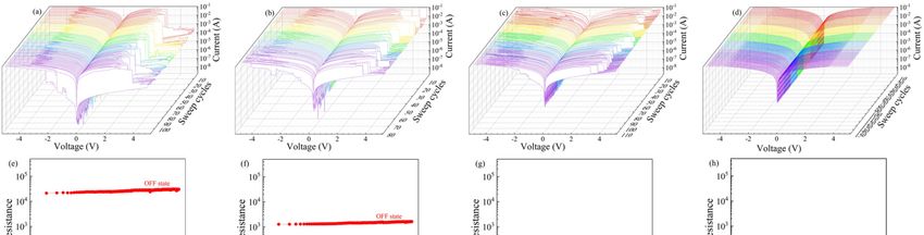
Nanomaterials 2021, 11, 2085                                                                                              3 of 11

                               pany (Suzhou, China). The egg albumen obtained from eggs was mixed with deionized
                               water at a ratio of 1:15 and ultrasonicated for 15 min. A mixture of 1.2 ωt%, 3 ωt%, and
                               6 ωt% MWCNTs and deionized water was treated by ultrasonication for more than 5 h to
                               uniformly disperse the MWCNTs in the liquid. The egg albumen solution and MWCNT
                               dispersion were prepared at a ratio of 1:1 by ultrasonication for 15 min until the mixture
                               was completely mixed. The mixed solution was spin-coated on glass coated with indium
                               tin oxide film, which was washed by ultrasonication for 15 min in alcohol, acetone, and
                               deionized water; the spin-coating method comprised an initial rotation speed of 500 rpm, a
                               rotation time of 5 s, a final rotation speed of 4000 rpm, and a rotation time of 60 s. The device
                               was dried at 105 ◦ C for 15 min, and the upper aluminium electrode was vapour-deposited
                               on the active layer. Finally, the device was annealed at 105 ◦ C for 15 min to complete the
                               fabrication of the Al/EA:MWCNT/ITO device.

                               2.2. Characterizations and Electrical Measurements of the Memristor
                                    Using a scanning electron microscope (SEM, Hitachi S3400) (Hitachi, Tokyo, Japan),
                               the cross section of EA: MWCNTs/ITO was observed. Energy dispersive spectroscopy
                               analysis of the chemical elements in the EA/ITO/glass and EA: MWCNTs/ITO/glass
                               was performed. An ultraviolet-visible (UV-Vis) spectrophotometer (UV/VIS, TU-1901)
                               (Puxi, Beijing, China) was used to measure the UV-Vis spectra of the egg film and MWCNT
                               film. A transmission electron microscope (TEM, JEM-2100) (JEOL, Tokyo, Japan) was
                               used to observe the microstructure of the MWCNTs. A semiconductor parameter tester
                               (Keithley 4200) (Keithley, Solon, OH, USA) was used to test the I-V characteristics of the
                               Al/EA:MWCNT/ITO device.

                               3. Results and Discussion
                               3.1. Device Structure and Material Characterization
                                     Figure 1a shows the egg white and yolk obtained from fresh eggs, and the albumen
                               liquid was collected in a centrifuge tube without any subsequent processing. Ovotransfer-
                               rin accounts for approximately 12–13% of the total egg protein [38], and Figure 1b shows
                               the three-dimensional ribbon model of the egg’s double ovotransferrin. It is a polymer
                               composed of 5284 protein atoms (yellow ribbons and yellow thread), tw trivalent iron ions
                               (two blue balls), and 132 water molecules (red dots) [39]. Figure 1c shows the structural
                               model of the Al/EA: MWCNT/ITO device and composite material based on MWCNTs and
                               egg albumen collected from glass vials. The diameter of each upper electrode is approxi-
                               mately 1.5 mm. Figure 1d shows a cross-section of the device under a scanning electron
                               microscope. The thickness of the active layer of the composite material of MWCNTs and
                               egg albumen is approximately 120 nm, and the thickness of the ITO layer is approximately
                               200 nm. The thickness of the Al electrode was approximately 200 nm, and the diameter of
                               each cell was approximately 1.5 mm. As shown in Figure 1e,f, the MWCNT film and egg
                               film were optically analysed by UV-visible spectroscopy. The wavelength corresponding
                               to Eg is obtained by the intersection of the edge tangent of the absorption peak and the
                               corrected baseline, so the absorption peak edges of the MWCNT film and the egg film are
                               at λ = 499 nm and λ = 589 nm, respectively. According to the equation Eg = hc/λ, the band
                               gaps of MWCNTs and eggs are approximately 2.48 eV and 2.11 eV, respectively. For the
                               calculation, Planck’s constant h = 6.62 × 10⁻³⁴ Js and the propagation speed of light in a
                               vacuum c = 3 × 10⁸ m/s were used [40].
                                     Figure 2a,b shows the EDS spectra of the EA/ITO/glass and EA: 1.2 ωt% MWC-
                               NTs/ITO/glass doped with carbon nanotubes. The peak value of C in the EA:1.2 ωt% film
                               is significantly higher than that in the EA film. In Figure 2c,d, the content of C in the film
                               increased from 0.4% to 8.61%, which proves that the carbon nanotubes were doped into
                               the egg white film. We also performed TEM mapping characterization tests on carbon nan-
                               otubes. Figure 2e,f show the microstructures of carbon nanotubes at different resolutions.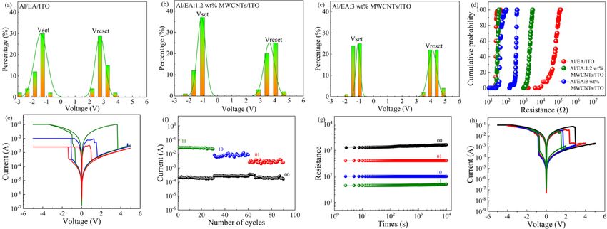
Nanomaterials 2021, 11, x FOR PEER REVIEW                                                                                  4 of 11

Nanomaterials 2021, 11, 2085                                                                                                                4 of 11
                                        2.11 eV, respectively. For the calculation, Planck’s constant h = 6.62 × 10⁻³⁴ Js and the prop‐
                                        agation speed of light in a vacuum c = 3 × 10⁸ m/s were used [40].

      FigureFigure
              1. (a) 1.The(a) egg
                              The white
                                   egg white
                                          andand yolk
                                              yolk of of
                                                      anan eggand
                                                         egg   andthe
                                                                   theegg
                                                                       egg white
                                                                           white taken
                                                                                  takenfrom
                                                                                        fromit.it.
                                                                                                (b)(b)
                                                                                                    Three−dimensional ribbon
                                                                                                       Three–dimensional      modelmodel
                                                                                                                           ribbon    of  of
            eggs with double egg transferrin. (c) Schematic configuration of the Al/EA: MWCNT/ITO device. (d) Cross−section of the
      eggs with
      Nanomaterials double egg transferrin. (c) Schematic configuration of the Al/EA: MWCNT/ITO device. (d) Cross–section of the
                    2021, 11, x FOR PEER REVIEW
            device. UV−Vis absorption spectra of the (e) MWCNT film and (f) egg albumen film.
                                                                                                                             5 of 11
      device. UV–Vis absorption spectra of the (e) MWCNT film and (f) egg albumen film.
                                              Figure 2a,b shows the EDS spectra of the EA/ITO/glass and EA: 1.2 ωt%
                                        MWCNTs/ITO/glass doped with carbon nanotubes. The peak value of C in the EA:1.2 ωt%
                                        film is significantly higher than that in the EA film. In Figure 2c,d, the content of C in the
                                        film increased from 0.4% to 8.61%, which proves that the carbon nanotubes were doped
                                        into the egg white film. We also performed TEM mapping characterization tests on carbon
                                        nanotubes. Figure 2e,f show the microstructures of carbon nanotubes at different resolu‐
                                        tions.

                                        3.2. Memristor Performance
                                             To study the influence of different concentrations of MWCNTs on the electrical char‐
                                        acteristics of Al/EA: MWCNT/ITO devices, the I‐V scanning characteristic curve of the
                                        devices was analysed. The scan voltage range was −5.00–5.00 V, and the limit current Icc
                                        was 0.1 A. Figure 3a shows that Al/EA/ITO and Al/EA: (1.2 ωt%, 3 ωt%, 6ωt%)
                                        MWCNT/ITO devices have bipolar resistance switching behaviour, and the switching cur‐
                                        rent ratio increases as the concentration of MWCNTs doped into the active layer de‐
                                        creases. Figure 3b shows the adjustability of the device switching current ratio. At a volt‐
                                        age of 0.1 V, the switching current ratios of the Al/EA/ITO and Al/EA: (1.2 ωt%, 3 ωt%,
                                        and 6 ωt%) MWCNT/ITO devices were 1.42 × 10³, 1.56 × 10², 14, and 1, respectively.
                                             As shown in Figure 4a–d, I‐V scanning of the same cell could be repeated more than
                                        100 times for the Al/EA/ITO and Al/EA: (3 ωt%, 6 ωt%) MWCNT/ITO devices, and scan‐
                                        ning of the Al/EA:1.2 ωt% MWCNT/ITO device could be repeated 70–80 times. Their
                                        switch ratio window size remained basically unchanged, and the high‐ and low‐resistance
                                        states were relatively stable. Figure 4e–h shows the measurement of the retention time of
                                        the four devices. Under a 1 V DC bias, the high and low resistance state.

                                     Figure 2.2.
                                     Figure     EDS spectra
                                                  EDS        of (a) of
                                                        spectra     EA/ITO/glass and (b) EA: and
                                                                       (a) EA/ITO/glass      1.2 ωt%
                                                                                                  (b)MWCNTs/ITO/glass. Element content
                                                                                                      EA: 1.2 ωt% MWCNTs/ITO/glass.    Element
                                     statistical analysis of (c) EA/ITO/glass and (d) EA: 1.2 ωt% MWCNTs/ITO/glass. TEM images of
                                     content statistical analysis of (c) EA/ITO/glass and (d) EA: 1.2 ωt% MWCNTs/ITO/glass. TEM
                                     MWCNTs: (e) low resolution and (f) high resolution.
                                     images of MWCNTs: (e) low resolution and (f) high resolution.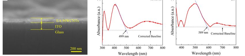
Nanomaterials 2021, 11, 2085                                                                                                                       5 of 11

                                      3.2. Memristor Performance
                                           To study the influence of different concentrations of MWCNTs on the electrical char-
                                      acteristics of Al/EA: MWCNT/ITO devices, the I–V scanning characteristic curve of the
                                      devices was analysed. The scan voltage range was −5.00–5.00 V, and the limit current
                                      Icc was 0.1 A. Figure 3a shows that Al/EA/ITO and Al/EA: (1.2 ωt%, 3 ωt%, 6 ωt%)
                                      MWCNT/ITO devices have bipolar resistance switching behaviour, and the switching cur-
                                      rent ratio increases as the concentration of MWCNTs doped into the active layer decreases.
                                      Figure 3b shows the adjustability of the device switching current ratio. At a voltage of 0.1 V,
                                                      Figure 2. EDS
                                      the switching current          spectra
                                                                 ratios       of (a)Al/EA/ITO
                                                                         of the      EA/ITO/glass and
                                                                                                   and(b) Al/EA:
                                                                                                          EA: 1.2 ωt% MWCNTs/ITO/glass.
                                                                                                                    (1.2 ωt%, 3 ωt%, andElement content
                                                                                                                                            6 ωt%)
                                                      statistical analysis of (c) EA/ITO/glass
                                                                                       3        and (d)
                                                                                                     2  EA: 1.2 ωt% MWCNTs/ITO/glass. TEM images of
                                      MWCNT/ITO devices were 1.42 × 10 , 1.56 × 10 , 14, and 1, respectively.
                                                         MWCNTs: (e) low resolution and (f) high resolution.

                               Figure 3.Figure
                                         (a) The 3.
                                                 I−V(a)
                                                     characteristics and (b) switchingand
                                                        The I–V characteristics        current
                                                                                           (b) ratio of Al/EA/ITO
                                                                                                switching         andratio
                                                                                                            current   Al/EA:
                                                                                                                           of(1.2 ωt%, 3 ωt%, and
                                                                                                                               Al/EA/ITO      and6Al/EA:
                                                                                                                                                  ωt%)
                               MWCNTs/ITO.
                                       (1.2REVIEW
       Nanomaterials 2021, 11, x FOR PEER   ωt%, 3   ωt%, and 6 ωt%) MWCNTs/ITO.                                                         6 of 11

                                           As shown in Figure 4a–d, I-V scanning of the same cell could be repeated more than
                                      100 times for the Al/EA/ITO and Al/EA: (3 ωt%, 6 ωt%) MWCNT/ITO devices, and
                                               Values after writing or erasing were relatively stable, and the holding time reached
                                      scanning   of the Al/EA:1.2 ωt% MWCNT/ITO device could be repeated 70–80 times. Their
                                         104 s, which reflects the strong holding ability of the device. As shown in Figure 4i–l, four
                                      switch  ratio  window size remained basically unchanged, and the high- and low-resistance
                                         devices were tested for voltage pulses. The pulse period was 2 ms, the duty cycle was 50%,
                                      states
                                         andwere    relativelywas
                                              the amplitude     stable.  Figure
                                                                   1 V. After  2.54e–h
                                                                                   × 104shows  the measurement
                                                                                         continuous                  of the
                                                                                                      pulses, the device stillretention  time of
                                                                                                                               had a clear
                                      thewrite/erase
                                          four devices.   Under
                                                      window,      a1V
                                                                which     DC bias,
                                                                        reflects     the high
                                                                                 the good      and low
                                                                                           durability     resistance
                                                                                                      of the device. state.

      FigureFigure  4. (a–d)
              4. (a–d)       The characteristics
                        The I–V  I−V characteristics under
                                                  under    continuous cycle
                                                         continuous   cycle scanning
                                                                            scanningand
                                                                                     and(e–h) thethe
                                                                                          (e–h)   retention times
                                                                                                     retention    and (i–l)
                                                                                                               times  and endurance
                                                                                                                            (i–l) endurance
            cycles of Al/EA/ITO and Al/EA: (1.2 ωt%, 3 ωt%, 6 ωt%) MWCNTs/ITO.
      cycles of Al/EA/ITO and Al/EA: (1.2 ωt%, 3 ωt%, 6 ωt%) MWCNTs/ITO.
                                               As shown in Figure 5a–c, the write/erase process and the stability of the high and low
                                          resistance states were tested and analysed. The SET voltage (Vset) and RESET voltage
                                          (Vreset) of the first 50 I‐V cycles of the Al/EA/ITO and Al/EA: (1.2 ωt%, 3 ωt%)
                                          MWCNT/ITO devices were statistically distributed on a histogram. The cumulative prob‐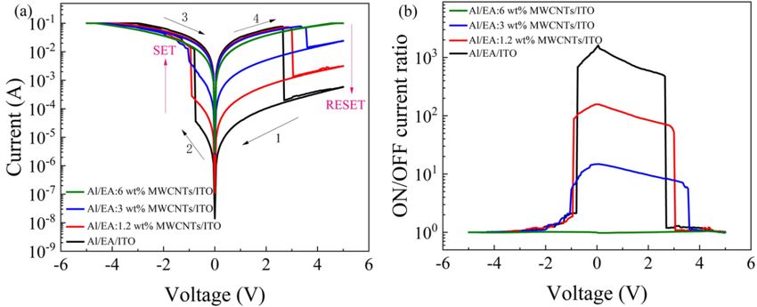
Nanomaterials 2021, 11, 2085 6 of 11
Values after writing or erasing were relatively stable, and the holding time reached
104 s, which
Nanomaterials 2021, 11, x FOR PEER REVIEW reflects the strong holding ability of the device. As shown in Figure 4i–l, 7 of 11
four
devices were tested for voltage pulses. The pulse period was 2 ms, the duty cycle was 50%,
and the amplitude was 1 V. After 2.5 × 10⁴ continuous pulses, the device still had a clear
write/erase
the window,
device, which whichmultilevel
achieved reflects the good
data durability
storage. of thecell
The same device.
of the device performed
As shown in
30 consecutive readFigure
and5a–c,
writethe write/erase
cycles process
at a voltage of 1and
V. the stability
Figure of the the
5g shows highretention
and low
resistance states
capability of the were testeddata
multilevel and storage
analysed.of The SETdevice,
the test voltageand (Vset)
theand
dataRESET voltage
were stable for(Vre-
104
set) of the first 50 I-V cycles of the Al/EA/ITO and Al/EA: (1.2 ωt%, 3 ωt%)
s under 1 V. The multilevel data storage mechanism indicates that the device would pro‐ MWCNT/ITO
devices
duce wereconductive
fewer statisticallyfilaments
distributed on aahistogram.
under The cumulative
larger limiting current. When probability of high
the number of
resistance state resistance
conductive filaments was reduced, (R HRS ) and low resistance state resistance
a smaller Vreset caused the device toLRS (R change shown
) are from a
in Figure
low 5d. The
resistance statemedian
to a highVset of the three
resistance state. devices was
Therefore, the−Vreset −1.08 V,
1.33 V,voltage and −1.08
decreased withV,
respectively, and the median Vreset was 2.70 V, 3.68 V and 4.13 V, respectively.
increasing the compliance currents, and the switching ratio decreased accordingly. As With the
increase
shown inin the concentration
Figure 5h, the deviceof MWCNTsread
maintained incorporated in the egg albumen
and write capabilities membrane,
under different scan
Vreset increased continuously, but the
voltage ranges to achieve low‐power storage. effect on Vset was small.
Figure 5. (a–c) Statistical distribution of Vset and Vreset
Vresetand
and(d)
(d)the
thecumulative
cumulativeprobability
probabilityofofthe
theresistance
resistanceofofAl/EA/ITO
Al/EA/ITO
and Al/EA: (1.2 ωt%, 3 ωt%) MWCNTs/ITO. (e–h) Al/EA: 1.2 ωt% MWCNTs/ITO: (e) I−V curve under different
and Al/EA: (1.2 ωt%, 3 ωt%) MWCNTs/ITO. (e–h) Al/EA: 1.2 ωt% MWCNTs/ITO: (e) I–V curve under different compliance compliance
currents, (f)
currents, (f) Continuous
Continuouscycle
cycleI–V characteristicsunder
I−Vcharacteristics underdifferent
differentcompliance
compliance currents,
currents, (g)(g) Four
Four state
state retention
retention characteris‐
characteristics,
tics, (h) I−V curve under different scanning voltage ranges.
(h) I–V curve under different scanning voltage ranges.
3.3. Mechanism
The median of Rthe Memristive Switch
HRS of the three devices was 7.18 × 10 Ω, 2.43 × 10 Ω and 4.05 × 10 Ω,
4 3 2
and the coefficients
To explore of variation
the current were 0.45,
transmission 0.22 and 0.14,
mechanism of the respectively.
device, the The median
I‐V scan curveRLRS
of
the 28.31 Ω,
wasdevice was34.80 Ω, andwith
redrawn Ω, andlogarithmic
49.44double the coefficients of variation
coordinates underwerenegative
0.11, 0.09, and 0.24,
voltage, as
respectively.
shown As the
in Figure 6a–c.concentration of MWCNTs
In a low resistance increased,
state (LRS), the degree
the slopes of dispersion ofdou‐
of the corresponding the
R
ble
HRS probability distribution decreased, and
logarithmic (I–V) curves of the device, Al/EA/ITO the R LRS of the Al/EA: 1.2 ωt% MWCNT/ITO
and Al/EA: (1.2 ωt%, 3 ωt%)
device was more
MWCNTs/ITO, areconcentrated
0.93, 0.99, and than
0.99,that of the other
respectively, whichtwoaredevices.
all closeTherefore,
to 1, and thethe con‐
egg
albumenbehaviour
duction RRAM with incorporated
of carriers in this MWCNTs
region obeys is more
Ohm’s reliable.
law [41]. In the low voltage range
of theInhigh
this resistance
paper, the state
coordinated
(HRS), Al/EA:MWCNT/ITO
the corresponding slopes device
are could achieve
1.22, 1.17, andmultilevel
1.04, and
dataregion
this storageis to improve the
represented as anstorage
ohmicdensity.
conductive Different
region. limiting
Undercurrents
the HRS can andbe setelectric
high on the
field with increasing voltage, the slopes are 1.90, 2.00, and 1.95, which are all close 2-bit
same unit of the device to obtain different switching current ratios, which realizes to 2.
memory.
This region Asisshown
expressedin Figure
as the5e, underlaw
Child’s a negative scanning
region, and voltage,
the current the Al/EA:
conforms to the1.2Mott–
ωt%
MWCNT/ITO
Gurney law. The device wastransmission
current set to different of limit currents
the device of 100 mA,
conforms 10 space
to the mA and 2.5 mA,
charge and
limited
the limit current of the positive scanning voltage was uniformly set
current (SCLC) model [42]. The whole HRS process completes the obvious transition from to 100 mA. The different
switchconductivity
ohmic ratios were 122, 30, and
to space 9. The RLRS
charge‐limited was largelyThis
conductivity. affected by theprocess
transition limitedconforms
current,
whereas the R HRS was basically unchanged. Figure 5f shows the stability
to the theoretical mechanism of space charge‐limited current transfer due to the existence and reliability of
the device, which
of traps [43,44]. achieved multilevel data storage. The same cell of the device performed
30 consecutive
Egg white read and write
is composed of cycles
88.5% at a voltage
water, 10.5%ofprotein,
1 V. Figureand 5g 1%shows the retention
carbohydrates and
capability
inorganic of
ions.the
At multilevel
present, data
158 storage
kinds of of the
proteins test
can device,
be and
identified,the data
includingwere stable for
ovalbumin,
104 s under 1 V.ovomucin,
ovotransferrin, The multilevel data storage
ovalbumin, globulin,mechanism
histone, and indicates
two orthat
morethe device
unique would
peptides
[45]. Ovotransferrin is an iron‐binding protein that is extremely sensitive to heat. The cap‐
ture/release of charge causes the oxidation/reduction of iron ions in ferritin. Using the
exchange characteristics of the ion itself, iron ions can be easily replaced by different kinds
of transition metal ions [46]. When a negative voltage is applied, electrons are injected into
the active layer through the upper electrode Al filling in the defects of charge trapping in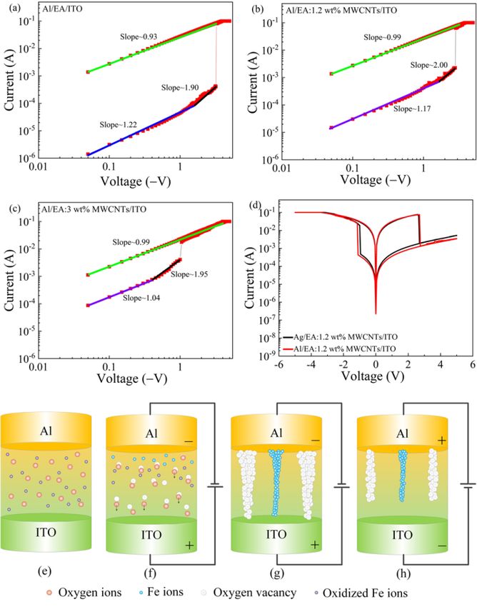
Nanomaterials 2021, 11, 2085                                                                                                   7 of 11

                                      produce fewer conductive filaments under a larger limiting current. When the number
                                      of conductive filaments was reduced, a smaller Vreset caused the device to change from
                                      a low resistance state to a high resistance state. Therefore, the Vreset voltage decreased
                                      with increasing the compliance currents, and the switching ratio decreased accordingly. As
                                      shown in Figure 5h, the device maintained read and write capabilities under different scan
                                      voltage ranges to achieve low-power storage.

                                      3.3. Mechanism of the Memristive Switch
                                           To explore the current transmission mechanism of the device, the I-V scan curve of
                                      the device was redrawn with double logarithmic coordinates under negative voltage, as
                                      shown in Figure 6a–c. In a low resistance state (LRS), the slopes of the corresponding
                                      double logarithmic (I–V) curves of the device, Al/EA/ITO and Al/EA: (1.2 ωt%, 3 ωt%)
                                      MWCNTs/ITO, are 0.93, 0.99, and 0.99, respectively, which are all close to 1, and the
                                      conduction behaviour of carriers in this region obeys Ohm’s law [41]. In the low voltage
                                      range of the high resistance state (HRS), the corresponding slopes are 1.22, 1.17, and 1.04,
                                      and this region is represented as an ohmic conductive region. Under the HRS and high
                                      electric field with increasing voltage, the slopes are 1.90, 2.00, and 1.95, which are all
                                      close to 2. This region is expressed as the Child’s law region, and the current conforms
                                      to the Mott–Gurney law. The current transmission of the device conforms to the space
                                      charge limited current (SCLC) model [42]. The whole HRS process completes the obvious
                                      transition from ohmic conductivity to space charge-limited conductivity. This transition
Nanomaterials 2021, 11, x FOR PEER REVIEW
                                      process conforms to the theoretical mechanism of space charge-limited current transfer due9 of 11
                                      to the existence of traps [43,44].

     Figure 6. (a–c) Al/EA/ITO andFigure         (a–c)ωt%,
                                       Al/EA:6. (1.2   Al/EA/ITO
                                                           3 ωt%) and  Al/EA: (1.2double
                                                                  MWCNT/ITO         ωt%, 3 ωt%)   MWCNT/ITO
                                                                                           logarithmic   fitting double
                                                                                                                  curves logarithmic fitting
                                                                                                                          of I‐V under  neg‐
                                      curves of  I–V  under negative bias. (d) I–V characteristics of Ag/EA:  1.2 ωt%
     ative bias. (d) I‐V characteristics of Ag/EA: 1.2 ωt% MWCNTs/ITO and Al/EA: 1.2 ωt% MWCNTs/ITO. (e–h) Resistance  MWCNTs/ITO       and
     switching mechanism model. Al/EA: 1.2 ωt% MWCNTs/ITO. (e–h) Resistance switching mechanism model.

                                    4. Conclusions
                                         In this paper, an Al/EA: MWCNT/ITO structured memristor was demonstrated. The
                                    current on‐off ratio and reset voltage of the device could be adjusted by changing the con‐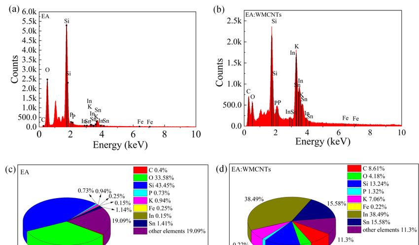
Nanomaterials 2021, 11, 2085                                                                                            8 of 11

                                     Egg white is composed of 88.5% water, 10.5% protein, and 1% carbohydrates and
                               inorganic ions. At present, 158 kinds of proteins can be identified, including ovalbumin,
                               ovotransferrin, ovomucin, ovalbumin, globulin, histone, and two or more unique pep-
                               tides [45]. Ovotransferrin is an iron-binding protein that is extremely sensitive to heat. The
                               capture/release of charge causes the oxidation/reduction of iron ions in ferritin. Using the
                               exchange characteristics of the ion itself, iron ions can be easily replaced by different kinds
                               of transition metal ions [46]. When a negative voltage is applied, electrons are injected into
                               the active layer through the upper electrode Al filling in the defects of charge trapping
                               in the amino acids broken down by the protein and acting as a space charge. Since the
                               work function difference between iron and aluminium or indium tin oxide electrodes
                               is relatively small, oxidized iron ions can easily obtain electrons and be reduced to iron
                               atoms. To explore whether the upper electrode of the device participates in the formation
                               of conductive filaments, the electrons were introduced to the oxidized iron ions, which
                               were easily reduced. We introduced Ag as the upper electrode to make Ag/EA: 1.2 ωt%
                               MWCNT/ITO devices and tested the IV curve, as shown in Figure 6d. The electrical
                               scanning characteristics of Ag/EA: 1.2 ωt% MWCNTs/ITO and Al/EA: 1.2 ωt% MWC-
                               NTs/ITO are consistent, which proves that the upper electrode does not participate in the
                               formation of conductive filaments.
                                     The resistance switching mechanism of the Al/EA:MWCNT/ITO devices can be
                               schematically explained as follows. As shown in Figure 6e, when no bias is applied, the
                               particles in the active layer are randomly distributed. When a negative bias is applied to
                               the upper electrode Al, electrons enter the active layer from the upper electrode Al to fill
                               the traps, and the oxygen ions in the active layer are affected by the electric field force and
                               move to the bottom electrode, leaving oxygen vacancies. Some of the oxidized iron ions
                               are affected by the electric field force and move to the upper electrode, where they are
                               reduced by electrons (Figure 6f). As shown in Figure 6g, as the applied negative voltage
                               increases, the electric field increases, generating an increasing number of oxygen vacancies
                               and iron atoms. Finally, a conductive filament that connects oxygen vacancies and iron
                               ions is formed between the upper and lower electrodes. At this time, the voltage reaches
                               Vset, and the device changes from an HRS to an LRS. When a positive bias is applied to
                               the upper electrode, the oxygen ions in the active layer are affected by the electric field
                               force and move to the upper electrode Al to continuously fill the oxygen vacancies, and
                               iron ions lose electrons and are further oxidized. As shown in Figure 6h, as the positive
                               voltage increases, the oxygen vacancies and iron ions are continuously reduced with the
                               enhancement of the electric field until the conductive filaments are destroyed. At this time,
                               the voltage reaches Vreset, and the device changes from an LRS to an HRS.
                                     MWCNTs have a strong ability to attract electrons, which can capture and transport
                               electrons in the active layer. When the Al electrode is negatively biased, the electrons
                               from the Al electrode and those in the active layer both fill the charge trapping centre
                               and are trapped by the MWCNTs. The electrons under low bias voltage do not have
                               enough energy/mobility to escape from the trapping centre [47]. The trapping centre is
                               the electron trap centre, that is, the oxygen vacancy [48]. When the voltage reaches Vset,
                               most of the charge trapping centres are filled with electrons, and the carriers increase
                               rapidly. Percolation pathways of charge carriers are formed between the upper and lower
                               electrodes, allowing electrons to jump between the MWCNTs and be transported along
                               them, and the device is transformed into an LRS. At this time, electrons can move freely
                               between the two electrodes, and the device forms a conductive filament [49]. After the
                               reverse voltage is applied, the electrons are removed from the trap, and the device changes
                               from an LRS to an HRS.
                                     The content of MWCNTs in the composite film and the distance between them de-
                               termine the trapping of carriers and the migration between MWCNTs. Therefore, as the
                               concentration of MWCNTs incorporated in the egg white membrane increases, the distance
                               between the MWCNTs decreases. The distance that electrons jump between MWCNTs
                               decreases, the number of electrons in the composite film increases, and the conductivity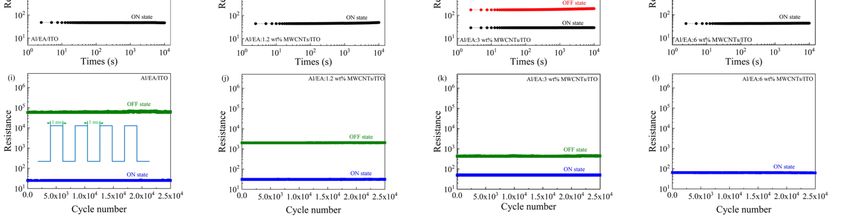
Nanomaterials 2021, 11, 2085                                                                                                                9 of 11

                                    of the RRAM increases. Due to the excessive content of MWCNTs, the Al/EA: 6 ωt%
                                    MWCNT/ITO devices did not exhibit resistance switching behaviour because they were
                                    densely packed in the composite film. This film could effectively transport charge carriers
                                    even under low bias, so that the device was always highly conductive.

                                    4. Conclusions
                                         In this paper, an Al/EA: MWCNT/ITO structured memristor was demonstrated.
                                    The current on-off ratio and reset voltage of the device could be adjusted by changing
                                    the concentration of MWCNTs in the active composite film. Al/EA/ITO devices and
                                    Al/EA:(1.2 ωt%, 3 ωt%, and 6 ωt%) MWCNT/ITO devices were fabricated. Analysis of
                                    their I-V characteristics proved that they could complete more than 100 consecutive bipolar
                                    resistance conversions in the same cell. The holding time reached 104 s under a voltage
                                    of 0.1 V, and the switching window remained clear under 2.5 × 10⁴ continuous pulses.
                                    Statistical analysis of the Vset, Vreset, RHRS , and RLRS of the device shows the improved
                                    reliability of the memristor formed by egg albumen doped with MWCNTs. The device can
                                    obtain different RLRS states by adjusting the limiting current, and the multilevel resistance
                                    realizes 2-bit data storage to increase the storage density. The data can be continuously
                                    rewritten/erased 30 times and kept for 104 s. The charge transfer mechanism of the device
                                    was based on the conductive principle of oxygen vacancy conductive filaments as well as
                                    iron atom conductive filaments. The increase in the concentration of carbon nanotubes
                                    resulted in an increase in the oxygen-containing functional groups, which promoted the
                                    formation of conductive channels to adjust the switching ratio of the device. In summary,
                                    Al/EA: MWCNT/ITO devices have excellent electrical characteristics, durability, stability,
                                    and reliability, allowing for potential applications in nonvolatile rewritable flash memory.

                                    Author Contributions: Data curation, T.Y.; Funding acquisition, L.W.; Investigation, L.W., T.Y. and
                                    D.W.; Methodology, L.W.; Visualization, T.Y.; Writing—original draft, L.W. and T.Y.; Writing—review
                                    and editing, L.W. All authors have read and agreed to the published version of the manuscript.
                                    Funding: This work was supported by the National Natural Science Foundation of China (Grant
                                    No. 61801174), Natural Science Foundation of Heilongjiang Province, China (Grant No. LH2021F045)
                                    and a Basic Research Project funded by the Basic Research Business Funding for Provincial Universi-
                                    ties in Heilongjiang Province (Grant No. KJCX201808).
                                    Conflicts of Interest: The authors declare no competing financial interests.

References
1.    Sokolov, A.S.; Abbas, H.; Abbas, Y.; Choi, C. Towards engineering in memristors for emerging memory and neuromorphic
      computing: A review. J. Semicond. 2021, 42, 013101. [CrossRef]
2.    Lee, T.H.; Hwang, H.G.; Woo, J.U.; Kim, D.H.; Kim, T.W.; Nahm, S. Synaptic Plasticity and Metaplasticity of Biological Synapse
      Realized in a KNbO3 Memristor for Application to Artificial Synapse. ACS Appl. Mater. Interfaces 2018, 10, 25673–25682.
      [CrossRef] [PubMed]
3.    Lee, A.R.; Bae, Y.C.; Baek, G.H.; Chung, J.B.; Lee, S.H.; Im, H.S.; Hong, J.P. Multifunctional resistive switching behaviors
      employing various electroforming steps. J. Mater. Chem. C 2016, 4, 823–830. [CrossRef]
4.    Dang, B.; Wu, Q.; Song, F.; Sun, J.; Yang, M.; Ma, X.; Wang, H.; Hao, Y. A bio-inspired physically transient/biodegradable synapse
      for security neuromorphic computing based on memristors. Nanoscale 2018, 10, 20089–20095. [CrossRef]
5.    Wu, S.; Ren, L.; Qing, J.; Yu, F.; Yang, K.; Yang, M.; Wang, Y.; Meng, M.; Zhou, W.; Zhou, X.; et al. Bipolar resistance switching in
      transparent ITO/LaAlO(3)/SrTiO(3) memristors. ACS Appl. Mater. Interfaces 2014, 6, 8575–8579. [CrossRef] [PubMed]
6.    Celano, U.; Nagashima, K.; Koga, H.; Nogi, M.; Zhuge, F.; Meng, G.; He, Y.; De Boeck, J.; Jurczak, M.; Vandervorst, W.; et al.
      All-nanocellulose nonvolatile resistive memory. NPG Asia Mater. 2016, 8, e310. [CrossRef]
7.    Hung, Y.-C.; Hsu, W.-T.; Lin, T.-Y.; Fruk, L. Photoinduced write-once read-many-times memory device based on DNA biopolymer
      nanocomposite. Appl. Phys. Lett. 2011, 99, 277. [CrossRef]
8.    Chu, H.-L.; Lai, J.-J.; Wu, L.-Y.; Chang, S.-L.; Liu, C.-M.; Jian, W.-B.; Chen, Y.-C.; Yuan, C.-J.; Wu, T.-S.; Soo, Y.-L.; et al. Exploration
      and characterization of the memcapacitor and memristor properties of Ni–DNA nanowire devices. NPG Asia Mater. 2017, 9, e430.
      [CrossRef]
9.    Hosseini, N.R.; Lee, J.-S. Biocompatible and Flexible Chitosan-Based Resistive Switching Memory with Magnesium Electrodes.
      Adv. Funct. Mater. 2015, 25, 5586–5592. [CrossRef]
Nanomaterials 2021, 11, 2085 10 of 11
10. Raeis-Hosseini, N.; Lee, J.S. Controlling the Resistive Switching Behavior in Starch-Based Flexible Biomemristors. ACS Appl.
Mater. Interfaces 2016, 8, 7326–7332. [CrossRef]
11. Hota, M.K.; Bera, M.K.; Kundu, B.; Kundu, S.C.; Maiti, C.K. A Natural Silk Fibroin Protein-Based Transparent Bio-Memristor.
Adv. Funct. Mater. 2012, 22, 4493–4499. [CrossRef]
12. Wang, L.; Wen, D. Nonvolatile Bio-Memristor Based on Silkworm Hemolymph Proteins. Sci. Rep. 2017, 7, 17418. [CrossRef]
13. Wang, H.; Meng, F.; Cai, Y.; Zheng, L.; Li, Y.; Liu, Y.; Jiang, Y.; Wang, X.; Chen, X. Sericin for resistance switching device with
multilevel nonvolatile memory. Adv. Mater. 2013, 25, 5498–5503. [CrossRef] [PubMed]
14. Zhou, G.; Yao, Y.; Lu, Z.; Yang, X.; Han, J.; Wang, G.; Rao, X.; Li, P.; Liu, Q.; Song, Q. Hydrogen-peroxide-modified egg albumen
for transparent and flexible resistive switching memory. Nanotechnology 2017, 28, 425202. [CrossRef] [PubMed]
15. Bok, C.H.; Woo, S.J.; Wu, C.; Park, J.H.; Kim, T.W. Flexible bio-memristive devices based on chicken egg albumen:Au@SiO2
core-shell nanoparticle nanocomposites. Sci. Rep. 2017, 7, 12033. [CrossRef] [PubMed]
16. Chen, Y.-C.; Yu, H.-C.; Huang, C.-Y.; Chung, W.-L.; Wu, S.-L.; Su, Y. Nonvolatile Bio-Memristor Fabricated with Egg Albumen
Film. Sci. Rep. 2015, 5, 1–12. [CrossRef]
17. Qu, B.; Lin, Q.; Wan, T.; Du, H.; Chen, N.; Lin, X.; Chu, D. Transparent and flexible write-once-read-many (WORM) memory
device based on egg albumen. J. Phys. D Appl. Phys. 2017, 50, 315105. [CrossRef]
18. Wang, L.; Wang, J.; Wen, D. Devices with Tunable Resistance Switching Characteristics Based on a Multilayer Structure of
Graphene Oxide and Egg Albumen. Nanomaterials 2020, 10, 1491. [CrossRef]
19. He, X.; Zhang, J.; Wang, W.; Xuan, W.; Wang, X.; Zhang, Q.; Smith, C.G.; Luo, J. Transient Resistive Switching Devices Made from
Egg Albumen Dielectrics and Dissolvable Electrodes. ACS Appl. Mater. Interfaces 2016, 8, 10954–10960. [CrossRef]
20. Wu, G.; Feng, P.; Wan, X.; Zhu, L.; Shi, Y.; Wan, Q. Artificial Synaptic Devices Based on Natural Chicken Albumen Coupled
Electric-Double-Layer Transistors. Sci. Rep. 2016, 6, 23578. [CrossRef]
21. Sung, S.; Park, J.H.; Wu, C.; Kim, T.W. Biosynaptic devices based on chicken egg albumen:graphene quantum dot nanocomposites.
Sci. Rep. 2020, 10, 1255. [CrossRef] [PubMed]
22. Yan, X.; Li, X.; Zhou, Z.; Zhao, J.; Wang, H.; Wang, J.; Zhang, L.; Ren, D.; Zhang, X.; Chen, J.; et al. A Flexible Transparent Organic
Artificial Synapse based on Tungsten/Egg Albumen/Indium Tin Oxide/polyethylene Terephthalate Memristor. ACS Appl. Mater.
Interfaces 2019, 11, 18654–18661. [CrossRef] [PubMed]
23. Zhu, J.X.; Zhou, W.L.; Wang, Z.Q.; Xu, H.Y.; Lin, Y.; Liu, W.Z.; Ma, J.G.; Liu, Y.C. Flexible, transferable and conformal egg albumen
based resistive switching memory devices. RSC Adv. 2017, 7, 32114–32119. [CrossRef]
24. Zhou, G.; Ren, Z.; Wang, L.; Sun, B.; Duan, S.; Song, Q. Artificial and wearable albumen protein memristor arrays with integrated
memory logic gate functionality. Mater. Horiz. 2019, 6, 1877–1882. [CrossRef]
25. Chang, J.W.; Wang, C.G.; Huang, C.Y.; Tsai, T.D.; Guo, T.F.; Wen, T.C. Chicken albumen dielectrics in organic field-effect transistors.
Adv. Mater. 2011, 23, 4077–4081. [CrossRef]
26. Jeon, D.-B.; Bak, J.-Y.; Yoon, S.-M. Oxide Thin-Film Transistors Fabricated Using Biodegradable Gate Dielectric Layer of Chicken
Albumen. Jpn. J. Appl. Phys. 2013, 52, 128002. [CrossRef]
27. Chen, J.; Liu, B.; Gao, X.; Xu, D. A review of the interfacial characteristics of polymer nanocomposites containing carbon
nanotubes. RSC Adv. 2018, 8, 28048–28085. [CrossRef]
28. Kanth, S.K.; Sharma, A.; Park, B.C.; Kim, H.S. Multiwalled carbon nanotube field emitter as an electron source for a microcolumn.
J. Vac. Sci. Technol. B Nanotechnol. Microelectron. Mater. Process. Meas. Phenom. 2016, 34, 011805. [CrossRef]
29. Ko, Y.; Kim, J.S.; Vu, C.C.; Kim, J. Ultrasensitive Strain Sensor Based on Pre-Generated Crack Networks Using Ag
Nanoparticles/Single-Walled Carbon Nanotube (SWCNT) Hybrid Fillers and a Polyester Woven Elastic Band. Sensors
2021, 21, 2531. [CrossRef]
30. Say, Y.; Guler, O.; Dikici, B. Carbon nanotube (CNT) reinforced magnesium matrix composites: The effect of CNT ratio on their
mechanical properties and corrosion resistance. Mater. Sci. Eng. A 2020, 798, 139616. [CrossRef]
31. Xu, R.; Wang, W.; Yu, D. A novel multilayer sandwich fabric-based composite material for infrared stealth and super thermal
insulation protection. Compos. Struct. 2019, 212, 58–65. [CrossRef]
32. Yang, H.; Lombardo, L.; Luo, W.; Kim, W.; Züttel, A. Hydrogen storage properties of various carbon supported NaBH4 prepared
via metathesis. Int. J. Hydrog. Energy 2018, 43, 7108–7116. [CrossRef]
33. Liu, G.; Ling, Q.-D.; Teo, E.Y.H.; Zhu, C.-X.; Chan, D.S.-H.; Neoh, K.-G.; Kang, E.-T. Electrical Conductance Tuning and Bistable
Switching in Poly(Nvinylcarbazole)-Carbon Nanotube Composite Films. ACS Nano 2009, 3, 1929–1937. [CrossRef] [PubMed]
34. Ageev, O.A.; Blinov, Y.F.; Il’in, O.I.; Kolomiitsev, A.S.; Konoplev, B.G.; Rubashkina, M.V.; Smirnov, V.A.; Fedotov, A.A. Memristor
effect on bundles of vertically aligned carbon nanotubes tested by scanning tunnel microscopy. Tech. Phys. 2013, 58, 1831–1836.
[CrossRef]
35. Liu, G.; Ling, Q.-D.; Kang, E.-T.; Neoh, K.-G.; Liaw, D.-J.; Chang, F.-C.; Zhu, C.-X.; Chan, D.S.-H. Bistable electrical switching
and write-once read-many-times memory effect in a donor-acceptor containing polyfluorene derivative and its carbon nanotube
composites. J. Appl. Phys. 2007, 102, 024592. [CrossRef]
36. Kim, K.; Chen, C.L.; Truong, Q.; Shen, A.M.; Chen, Y. A carbon nanotube synapse with dynamic logic and learning. Adv. Mater.
2013, 25, 1693–1698. [CrossRef]Nanomaterials 2021, 11, 2085 11 of 11
37. Molinari, F.N.; Barragán, E.; Bilbao, E.; Patrone, L.; Giménez, G.; Medrano, A.V.; Tolley, A.; Monsalve, L.N. An electrospun
polymer composite with fullerene-multiwalled carbon nanotube exohedral complexes can act as memory device. Polymer 2020,
194, 122380. [CrossRef]
38. Wu, J.; Acero-Lopez, A. Ovotransferrin: Structure, bioactivities, and preparation. Food Res. Int. 2012, 46, 480–487. [CrossRef]
39. Kurokawa, H.; Mikami, B.; Hirose, M. Crystal Structure of Diferric Hen Ovotransferrin at 2.4 Å Resolution. J. Mol. Biol. 1995, 254,
196–207. [CrossRef] [PubMed]
40. Zhigunov, D.M.; Kamaev, G.N.; Kashkarov, P.K.; Volodin, V.A. On Raman scattering cross section ratio of crystalline and
microcrystalline to amorphous silicon. Appl. Phys. Lett. 2018, 113, 023101. [CrossRef]
41. Walke, P.D.; Rana, A.; Yuldashev, S.U.; Magotra, V.K.; Lee, D.J.; Abdullaev, S.; Kang, T.W.; Jeon, H.C. Memristive Devices from
CuO Nanoparticles. Nanomaterials 2020, 10, 1677. [CrossRef] [PubMed]
42. Ismail, M.; Abbas, H.; Choi, C.; Kim, S. Stabilized and RESET-voltage controlled multi-level switching characteristics in ZrO2-
based memristors by inserting a-ZTO interface layer. J. Alloy. Compd. 2020, 835, 155256. [CrossRef]
43. Kang, W.; Woo, K.; Na, H.B.; Kang, C.J.; Yoon, T.S.; Kim, K.M.; Lee, H.H. Analog Memristive Characteristics of Square Shaped
Lanthanum Oxide Nanoplates Layered Device. Nanomaterials 2021, 11, 441. [CrossRef] [PubMed]
44. Min, S.Y.; Cho, W.J. High-Performance Resistive Switching in Solution-Derived IGZO:N Memristors by Microwave-Assisted
Nitridation. Nanomaterials 2021, 11, 1081. [CrossRef] [PubMed]
45. Mann, K.; Mann, M. In-depth analysis of the chicken egg white proteome using an LTQ Orbitrap Velos. Proteome Sci. 2011, 9, 1–6.
[CrossRef]
46. Ko, Y.; Kim, Y.; Baek, H.; Cho, J. Electrically Bistable Properties of Layer-by-Layer Assembled Multilayers Based on Protein
Nanoparticles. ACS Nano 2011, 5, 9918–9926. [CrossRef]
47. Sun, Y.; Miao, F.; Li, R. Bistable electrical switching and nonvolatile memory effect based on the thin films of polyurethane-carbon
nanotubes blends. Sens. Actuators A Phys. 2015, 234, 282–289. [CrossRef]
48. Russo, P.; Xiao, M.; Zhou, N.Y. Carbon nanowalls: A new material for resistive switching memory devices. Carbon 2017, 120,
54–62. [CrossRef]
49. Xin, Y.; Zhao, X.; Zhang, H.; Wang, S.; Wang, C.; Ma, D.; Yan, P. Bistable electrical switching and nonvolatile memory effect in
poly (9,9-dioctylfluorene-2,7-diyl) and multiple-walled carbon nanotubes. Org. Electron. 2019, 74, 110–117. [CrossRef]You can also read