International Electrostatic Discharge Workshop May 17-20, 2021
←
→
Page content transcription
If your browser does not render page correctly, please read the page content below

International Electrostatic
               Discharge Workshop
2021

               May 17-20, 2021
               Special Virtual Event

               IEW
              Setting the Global Standards for Static Control!
EOS/ESD Association, Inc. 7900 Turin Rd., Bldg. 3 Rome, NY 13440-2069, USA
        PH +1-315-339-6937 • Email: info@esda.org • www.esda.org
IEW 2018 Turnout Belgium

Management Committee                           Technical Program Committee
Management Committee Chair
Steffen Holland, Nexperia                      Dietmar Walther, Texas Instruments
Technical Program Chair                        Deutschland GmbH
Heinrich Wolf, Fraunhofer EMFT                 Kai Esmark, Infineon Technologies AG
Keynote Chair                                  Nathan Jack, Intel
Theo Smedes, NXP Semiconductors                Christian Stockreiter, ams AG
Invited Speaker and Seminar Chair:             Evan Grund, Grund Technical Solutions
Shih-Hung Chen, imec                           Dolphin Abessolo Bidzo, NXP Semicon-
                                               ductors
Discussion Group and Special Interest Group
Chair                                          Rita Fung, Cisco
Fabrice Caignet, LAAS/CNRS                     Andrea Boroni, STMicroelectronics
Audio/Visual Chairs
Vasantha Kumar, Nexperia
Paul Phillips, Phasix
Industry Council Advisor
Harald Gossner, Intel Deutschland GmbH
EOS/ESD Association, Inc. Operations Chair
Christina Earl
EOS/ESD Association, Inc. Director of Events
Nathaniel Peachey, Qorvo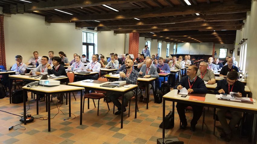
Experience IEW
Greetings from the 14th annual International ESD Workshop (IEW) Management Team! This
event presents a unique opportunity for attendees to participate in in-depth discussions and
learning on EOS and ESD topics in a highly interactive virtual environment. This virtual event
will be held via Microsoft Teams and Spatial Chat
Focused discussion groups, held in the afternoons, are a unique part of our interactive
workshop. While each EOS/ESD topic discussion is facilitated by an expert on the subject, the
main discussion will take place among the participants. The discussion groups will address
topics of the focus issues and include ESD soft failures, challenges for advanced CMOS
ESD protection, System level test for IOT and wearable devices, latch-up, on-chip health
monitoring strategies and the effects if CDM limits are lowered to 150 volts.
Scheduled poster sessions are the core of the technical program. These poster sessions
begin with a brief introduction of each contribution by the authors to the workshop
participants. These teasers encourage the participants to visit each poster and its author in
the subsequent interactive poster discussion session. To compliment the offering, attendees
are also encouraged to bring open posters. This format provides an ideal forum for learning
and the interchange of new ideas. Topics covered in the poster sessions include CDM effects
and failures, Test cases, ESD verification with EDA tools, ESD devices for advanced CMOS
technology, models for SEED simulations, on-chip ESD protection devices, latch-up and
interconnect investigations.
Stimulating state-of-the-art EOS/ESD seminars, as well as invited talks are scheduled. Come
and listen to presentations, and later meet with the presenters, discussing ESD protection for
brain implantable electronics, FD-SOI technology, fast transients of CDM, side channel attacks
on chips with security functions, ESD qualification methods of automotive manufacturers,
EMC design and soft failures, electrical overstress and new IEC testing results.
Come and meet experts, share your views, ask questions, and extend your network with EOS/
ESD experts from industry and academia. Above all, learn how to efficiently deal with today’s
EOS/ESD challenges and prepare for tomorrow in an informal and interactive atmosphere.
Register for this event early. This will help us in the final planning and preparation for an
extraordinarily successful event. We sincerely hope that you will join us virtually for the 2021
IEW.

For poster sessions, workshops, and networking, virtual attendees can use
Spatial Chat. Spatial Chat is a video chat conversation platform that recreates
real-life social interactions. Please visit https://spatial.chat/ to get familiar with
the program. Access to the IEW spatial chat will be sent to attendees before the
event.

                                                                                           3
Tutorial Monday 13:00 - 15:00
Advanced TLP Applications
Instructor: Heinrich Wolf, Fraunhofer EMFT

The tutorial covers accuracy aspects of transmission line testing and explains how
to do characterization and parameter extraction for compact modelling including
switching behavior and electro-thermal aspects. Furthermore, it discusses SOA
measurements and the application of CC-TLP as a CDM like stress method.
                   Heinrich Wolf received his diploma degree in electrical engi-
                   neering from the Technical University of Munich (TUM) and his
                   PhD from the Technical University of Berlin, Germany. He joined
                   the chair of integrated circuits at TUM as a member of the sci-
                   entific staff working on electrostatic discharge related issues.
                   This involved modeling of ESD-protection elements, parameter
                   extraction techniques, and test chip design. In 1999, he joined
                   the Munich branch of the Fraunhofer Institute for Reliability and
Microintegration (IZM) which became the Fraunhofer Institution for Microsystems
and Solid State Technologies EMFT in 2010. He was involved in the investigation
of ESD protections for CMOS and smart power technologies. Furthermore, he
worked on the simulation and development of ESD protections and on the devel-
opment of ESD test methods and tester characterization. He is also coordinating
the ESD related activities at the EMFT including the development of ESD test
systems and the design of protection structures for deep submicron technologies.
Furthermore, he works in the field of RF simulation and characterization in the
frequency range up to 110 GHz. Currently he also represents the german ESD-Fo-
rum in the standards working groups.

Monday Entertainment 16:45 - 17:45
Chocolate Tasting “from 0 to 100 in 10 Chocolates"
This relaxing evening event is a culinary chocolate trip with Oliver Rohl from
Schokovida in Hamburg. Attendees will enjoy a presentation about the whole world
of chocolate while sampling everything from white to whole milk, plain and dark
chocolate, truffle, and bar chocolate as well as cocoa beans. Everything is made
by hand with high-end ingredients and a love of the trade.
Attendees who register early will have chocolate mailed to them to enjoy
during this presentation. Attendees registering late will receive choclate af-
ter the event.
Keynote
ESD Protection for Medical Implants
Wolfgang Krautschneider, Hamburg University of Technology

Scaling-down of CMOS circuits is accompanied by a huge performance increase of in-
tegrated circuits that opens up much potential of electronics for medical implants. There
are already some electronic implants in use, e.g., pace makers, cochlear implants and
implants for deep brain stimulation. Implants for other medical applications are in an early
state or under development.
Biological signal sources show in most cases a very high impedance and provide sig-
nals with a very low amplitude. This requires amplifiers with very high input impedance
provided by MOS transistors. For handling the electronic circuits during assembly, all the
pads connected to gates of MOS transistors have to be protected by ESD devices that
may degrade the input resistance resulting in worse signal to noise ratios. An appropriate
trade-off has to be found that will be illustrated by demonstrators for medical implants.
Another challenge for medical implants are the very high magnetic fields of MRI which
may generate high voltages that have to be handled by protection structures.
One out of four persons in western countries gets the diagnosis cancer with metastases.
They are treated by systemic therapy (chemotherapy etc.) combined with radiotherapy
applying comparably high radiation doses. When these patients carry medical implants,
the radiation can degrade the characteristics of ESD protection devices, so that design
measures have to be taken to adjust their radiation robustness accordingly.

                         Wolfgang H. Krautschneider (M’85) received the M.Sc., Ph.D., and Habil-
                         itation degrees from the Berlin University of Technology, Berlin, Germa-
                         ny.,He was with Central Research Laboratories, IBM, Yorktown Heights,
                         NY, USA, the Siemens Research Center, Munich, Germany, and the
                         DRAM Project of IBM and Siemens, Essex Junction, VT, USA. He is cur-
                         rently the Head of the Institute of Nanoelectronics at the Hamburg Univer-
                         sity of Technology, Hamburg, Germany.
Invited Talks
Invited Speaker Chair:
Shih-Hung Chen, imec

Invited talks always give good opportunities to broaden workshop attendees’ exposure to expertise in different fo-
cused areas of interests. This year, three invited talks are included with wide-range aspects from process technol-
ogy, chip security, to system qualification. The talk from Dr. Philippe Galy, STMicroelectronics, is one of the focus
topics of this year. It is dedicated to ESD/LU challenges for ultra-thin body and box (UTBB) fully depleted SOI (FD
SOI) CMOS technology for 2D and 3D innovative solutions. Dr. Galy will give an introduction of this UTBB FD SOI
technology and will also discuss innovative ESD solutions. The talk from Alexander Schlösser, NXP, will focus on
side channel attacks for high security automotive chips. In this talk, Alexander will look at how hardware security
analysis uses soft failures and will explore the differences and similarities to ESD-related failures. The talk from
Dimitri Linten, imec, will focus on the scaling technology with system technology co-optimization (STCO) approach
toward node N5 and beyond. Dr. Linten will give an introduction of the novel STCO approach and will discuss the
ESD reliability challenges in this technology.

Invited Talk 1
UTBB FD-SOI and ESD/Latch-up: Challenges and Solutions
Philippe Galy, STMicroelectronics
This talk is dedicated to ESD/LU challenges for Fully Depleted SOI (FD-SOI) Ultra Thin Body and Box (UTBB)
CMOS technology nodes for 2D and 3D innovative solutions. After an introduction on the UTBB FD_SOI technol-
ogy provided by STmicrolectronics, especially in 28nm High k metal gate, the ESD protection challenges in this
technology will be discussed along with solutions. Preliminary silicon results with 2D/3D innovative solutions are
introduced according to performance and integration. Moreover, radiation effects are also addressed.

                    Philippe Galy born 1965, received the Ph.D. from University of Bordeaux and H.D.R from
                    LAAS CNRS University of Toulouse. He is a fellow, technical director at STmicrolectronics
                    Research and Development France. He has proposed a full CDM protection and several
                    new ESD compact devices for mature & advanced CMOS technologies. He supports sev-
                    eral teams for research focused on new innovative solutions: Memory + silicon Qubit and
                    cryo-design, Neuromorphic, 3D ultimate integration. He has authored or coauthored several
                    publications (+100), books (3), and patents (+100). He serves in TPC and is a reviewer for
                    many symposiums and journals. He is also involved in National (3) and European projects (4).
                    Also he joins the QuEng CDP team from Grenoble and also adjunct professor at “ Université
                    de Sherbrooke (UdS)”.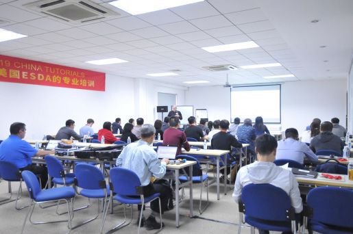
Invited Talk 2
Reliability Challenges in Scaling Era with System Technology Co-Optimization
(STCO) Approach
Dimitri Linten, imec
From the 10 nm technology generation onward, traditional scaling has been complemented by design-technology
co-optimization (DTCO), combining expertise from technology as well as from design. But, as the technology mov-
ing forward, the benefits of DTCO in system-on-chip (SoC) applications are expected a certain saturation. For 3 nm
and beyond technology nodes, the focus will shift from scaling at logic cell level towards scaling at system level.
Hence, DTCO is evolving into an system technology co-optimization (STCO)-oriented approach. More and more
(sub-)system functions will be integrated in one chip with a special 3D vertically stacked or 2.5D interposer architec-
ture. However, a chip-level or even a system-level electrical reliability becomes necessary to evaluate at the early
stage of the technology/circuit/system development period.
In this talk, we will look at the technology features of the STCO approach, including different 3D integration technol-
ogies applied in different levels of interconnect hierarchy. In addition, the emerging reliability challenges will be also
discussed from different aspects in the STCO framework. .
                        Dimitri Linten received PhD degrees in electrical engineering from the Vrije Universi-
                        teit Brussel (VUB), Brussels, Belgium in 2006. Since 2015, he is the R&D manager
                        of the Device Reliability and Electrical characterization group at imec. He is a senior
                        member of the IEEE (SM13). His main research interests are ESD reliability, Mem-
                        ory and logic device reliability physics, radiation, biosensors and security. He has
                        served as a technical program committee member of several international scientific
                        conferences, among which the International Reliability Physics Symposium (IRPS),
                        the EOS/ESD Symposium, the International ESD Workshop (IEW) and International
                        Electron Devices Meeting (IEDM).

Invited Talk 3
Soft Fails as a Tool in Hardware Security Analysis
Alexander Schlösser, NXP Semiconductors
While soft fails are to be avoided from an ESD point of view they can be quite useful in another domain. Hardware
Security Analysis is a specific field in the wide world of hacking and penetration testing. It focuses largely on so-
called implementation attacks, targeting the unintended imperfections and compromises in the physical realization
of a digital design. The methods for these attacks are often derived from failure analysis and include the use of
lasers, micro- and nano-probes as well as small-scale antennas and field generators.
A specific group of methods are Fault Injection Attacks. These are active but non-invasive efforts to intentionally
cause soft fails, with the aim to compromise the secure handling of to-be-protected data. This talk will introduce the
systems and methods used in fault injection attacks and the physical effects and interactions that are exploited. It
will show how hardware security analysis uses these fails and discuss differences and similarities to ESD-related
fails.

                       Alexander Schlösser is a Senior Security Analyst with NXP Semiconductors. As a member
                       of NXP’s internal hacking team he conducts hardware security analyses of Smart Cards
                       and Secure Elements as well as automotive and application processors. Alexander has a
                       background in photonics and received a PhD in physics from TU Berlin before he joined
                       NXP in 2014. Since then he develops systems and methods to identify and root-cause vul-
                       nerabilities and weaknesses in digital designs with a security focus.

                                                                                                                   7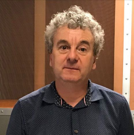
Seminars
Seminar Chair:
Shih-Hung Chen, imec

Four recognized experts from university, research institute, and industry will give seminar talks on some of the
highly interesting topics at this year’s IEW. These seminar talks are covered with the main ESD challenges in
system-level, component-level, and even manufacturing perspectives. The seminar from Dr. Wolfgang Stadler,
Intel, will focus on non-standard overstress in manufacturing phase and will show the (mis)correlation between
IC ESD qualification waveforms and real world risks in handling ICs, boards, and systems. The seminar from
Professor David Pommerenke, ESDEMC, will focus on system-level ESD testing and will discuss the reasons
for large uncertainty of the test results even when carefully following the procedures in IEC 61000-4-2, as well
as give suggestions to the test implementation. The seminar from Professor Franco Fiori, Politecnico di Torino,
will focus on circuit-level EMC/EMI design and will discuss recent progresses on the EMI immune designs of
MEMS readout circuits. Finally, the seminar from Johannes Weber, Fraunhofer EMFT, will focus on fast transient
of CDM ESD event and will cover wide-range perspectives of the fast rise time (or fast slew rate) from the fun-
damental theory to the testing methodologies.

Seminar 1                                                                         Dr. David Pommerenke received
                                                                                  his diploma and PhD from the
Achieving Meaningful and Repeatable Re-                                           Technical University Berlin,
sults in ESD System Level Testing                                                 Germany. His research interests
                                                                                  are system level ESD, electronics,
David Pommerenke, Technical University of Graz.
                                                                                  numerical simulations, EMC
The vast majority of system level ESD testing follows the                         measurement methods and
specifications defined in IEC 61000-4-2. Unfortunate-          instrumentation. He worked at Hewlett Packard
ly, even when carefully following the procedures in IEC        for 5 years before joining the electromagnetic
61000-4-2 there is a high level of uncertainty in the test     compatibility laboratory at the Missouri University
results, and successful passing of the test requirements is    of S&T in 2001. Dr. Pommerenke became the CTO
often not a good prediction of ESD robustness in the field.    of ESDEMC in July 2019 before joining the ESD/
The talk, which is based on a white paper by the Industry      EMC group at the Technical University of Graz in
Council on ESD Target Levels explains deficiencies of the      Austria in January 2020. His new focus is on ESD,
standard and problems within the generally applied test        EMC, harmonics, and PIM. He has published more
procedures. Based on this analysis the talk suggests im-       than 200 papers and is inventor on 13 patents.
provements to both the standard, and the test implemen-        His main research interests are measurement/
tation.                                                        instrumentation ESD, electronic design and EMC.
This includes                                                  He is IEEE fellow and associated editor for the IEEE
 - better ESD gun specifications                               Transactions on EMC.
 - Full wave and SPICE models for ESD generators
 - Simulation of ESD robustness following the SEED con-
cept (System Efficient ESD Design)
 - Improved documentation, such as measuring the ESD
current during testing
  - Improved test produced e.g., number of discharges,
methods of stabilizing the arc in air discharge etc.
 - Robotic ESD testing
The goal of the talk is to explain the reasons for the large
test result uncertainty, to give suggestions to the standard
committee for improvements and to enable engineers to
implement the test in such a way that results are mean-
ingful, repeat well and give indications for the root cause
of a failure.
Seminar 2                                                        Seminar 3
Correlation of Qualification ESD Robust- Recent Advances on the Design of
ness and Handling Threats                MEMS Readout Circuits Immune to
Wolfgang Stadler, Intel Deutschland GmbH EMI
                                                                 Franco Fiori, Politecnico di Torino
Today, almost all integrated circuits (ICs) are qualified with
respect to Human Body Model (HBM) and Charged Device             Among the circuit topologies available in the open
Model (CDM). Current international standards on ESD Con-         literature for the design of MEMS readout circuits,
trol Programs require a minimum ESD robustness of 100 V          those based on the current feedback differential
according to HBM and 200 V of CDM for ICs to ensure safe         difference amplifier (DDA) are usually preferred
handling. However, there is no clear correlation between         because they feature a wider differential input
qualification waveforms and waveforms of reel ESD events         range (DMIR), rail-to-rail common mode input
even on IC level, therefore, the qualification might not nec-    range (CMIR), high power supply rejection (PSR)
essarily cover all problems.                                     as well as high noise figure. These are valuable
The situation is even worse if ESD events on system lev-         features for low voltage applications. In addition,
el are considered. Such events mainly occur during board         such a topology lends itself well to implement aux-
and system assembly or during testing, like Charged Board        iliary circuits such as those needed for input bias-
Events, Cable Discharge Events, or transient latch-up. To-       ing or DC offset cancellation or AC calibration.
day, there are no widely accepted ESD qualification stan-
dards on most of these ESD system level events, this is
one reason why the ESD control standards refer to IC level                        Franco Fiori(M’02) received the
robustness only.                                                                  Laurea and Ph.D. degrees in
In this presentation, we will assess the (mis)correlation be-                     electronic engineering from the
tween IC ESD qualification waveforms and real world risks                         Polytechnic University of Turin,
in handling ICs, boards, and systems. We will also discuss                        Turin, Italy, in 1993 and 1997,re-
which ESD system level characterization methods could                             spectively. From 1997 to 1998,
help to improve the ESD process assessment methodolo-                             he was an R&D Leader ofST-
gies of boards or system handling processes.                                      Microelectronics, Milan, Italy. In
                                                                                  1999, he joined the Electronics
                                                                 and Telecommunication Department, Polytech-
                    Wolfgang      Stadler    received    his
                                                                 nic University of Turin, where he is currently an
                    diploma degree in physics in 1991
                                                                 Associate Professor of Electronics. From 2006 to
                    and in 1995 the PhD degree from the
                                                                 2010, he was the Scientific Leader of a joint ST-
                    Physics Department of the Technical
                                                                 Microelectronics-Politecnico di Torino Research
                    University Munich. 1995 he joined the
                                                                 Laboratory aimed to investigate chip-level EMC
                    semiconductor division of Siemens,
                                                                 issues. He has authored and coauthored more
                    which became Infineon Technologies
                                                                 than 170 papers published in international jour-
                    in 1999. His focus was on development
                                                                 nals and conference proceedings. His research
                    of ESD-protection concepts in CMOS
                                                                 interests include analog circuit design, mac-
technologies and on innovative ESD topics. In this role he       ro-modeling of active nonlinear circuits, smart
was coordinator of several European and German ESD               power devices, and electromagnetic compatibil-
funding projects. Since 2003, he was also been responsible       ity.
for the measurement characterization of I/O cells and PHYs.
In 2011, he joined Intel Mobile Communications which is
now Intel Deutschland GmbH. Within the corporate quality
network, he is currently responsible for the ESD control
program of Intel and for ESD risk assessment. Furthermore,
he supports ESD/latch-up testing and qualification of
products. Wolfgang holds several patents in ESD-related
topics. He is author or co-author of more than 120 technical
papers and has co-authored a book on ESD simulation.
He has received several best paper awards and teaches
courses on ESD device testing, ESD qualification, and
ESD control measures (for example, TR53 ESD Technician
Certification).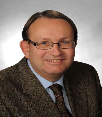
Seminar 4
Stress Current Rise Time Evaluation in
the Single-Digit Picosecond-Domain
Johannes Weber, Fraunhofer EMFT
This seminar will cover theory including the definition
of rise time/slew rate, relation to bandwidth oft the
test system, and voltage overshoot of typical ESD
protection schemes; as well as dependency of ESD
robustness (peak current failure thresholds) on rise
time (slew rate). Examples of discharges with ultra-
fast rise times in the manufacturing line will be given.
The seminar will also include discussion on current
rise time evaluation of CDM testing and alternative
contact-based test method CC-TLP as a method to
repeatably control rise time of stress pulses. During
the seminar, the speaker will challenge the limits
of today’s test methods and methodologies in the
single-digit picosecond domain and discuss critical
parameters that may influence the slew rate (rise time)
sensitivity of high-speed devices (high-speed design,
DC-blocking capacitor etc.).

                    Johannes Weber received his
                    Master’s degree in physics from
                    the Technical University Munich
                    (TUM) in 2015. He wrote his
                    Master’s thesis in the research
                    area of Nuclear, Particle and
                    Astrophysics at the Max Planck
                    Institute for Extraterrestrial Physics
                    (MPE). Afterward, he joined the
                    Team of Analysis & Test at the
Fraunhofer Research Institution for Microsystems and
Solid State Technologies EMFT in Munich, Germany
as a research associate. He works in the field of
Electrostatic Discharges (ESD) and focuses on the
development of ESD test methods and ultra-fast ESD
events in the picosecond domain. His research mainly
deals with the influences of critical stress parameters
like the rise time or the energy content of the stress
pulse on the failure level of advanced semiconductor
technologies. Supported by the ERC Grant 2016 of the
ESD-Association, he finished his PhD thesis with the
title “Pulsed High Current Characterization of Highly
Integrated Circuits and Systems” at the Bundes-wehr
University of Munich in 2019.
Discussion Groups
Discussion Groups Chair:
Fabrice Caignet, LAAS/CNRS
The discussion groups are an integral part of the workshop. There will be six discussion groups offered,
with three parallel sessions on Tuesday evening and three parallel sessions on Wednesday evening. The
topics include ESD soft failures; ESD challenges for advanced CMOS (FD-SOI, beyond FINFETS); discus-
sions on health monitoring, the appropriateness of system level testing for IoT devices/wearables; latch-
up; and testing devices for CDM below 150 volts. Each discussion group has a moderator with extensive
expertise on the topic to help guide and inspire the discussion. The success of these sessions depends on
your active participation. We encourage you to bring along data, ideas, and other items of interest to share.
Session A
Parallel Groups-Tuesday 16:30-18:00
DG A.1 DG A.2
ESD Challenges for Advanced CMOS (FD-SOI, System Level Test: is it Appropriate for IOT
Beyond FINFETS) Devices/Wearables?
Co-Moderators: Shih Hung Chen, imec; Philippe Galy, Co-Moderators: Adrijan Barić, University of Zagreb
STMicroelectronics Faculty of Electrical Engineering and Computing; Har-
ald Gossner, Intel Deutschland GmbH
While Bulk FinFET and Fully-Depleted (FD) SOI
technologies have become the mainstream in the ad- System level testing using IEC 61000-4-2 is like an
vanced CMOS IC industry, what are the next technol- elephant in a glass shop; it seems to be widely ap-
ogy options or next device architectures after FinFET plicable and it produces sound results. However,
and FD SOI? Several promising candidates have the question is, is it really useful and relevant for
been proposed; however, only very few prior works real world events or is there any better approach?
discussed ESD reliability in these promising future Also, what are the most appropriate test levels for
technologies. In addition, the challenges might not tiny IoT devices. Are the size of the IoT device and
only from technology options but also from more real- the technology node critical for the energy that can
istic aspects, such as design verification and product be dissipated on the device? What are the ulti-
qualification. This discussion group aims to look at mate sustainable testing levels for the down scaled
the ESD challenges in advanced CMOS technologies technology nodes that will inevitably penetrate into
with varied perspectives. With your ideas and sharing the IoT market? Finally, when we do system level
experience, this discussion group will be able to bring testing, do we look only for the functionality of the
some clarity to those emerging ESD challenges. device or we also have to worry about safety of
the system. Is it possible to disturb the operation in
such a way that the data sent from IoT device can
generate a twisted image of the reality?DG A.3 Is Latch-up Testing Still Relevant? Moderator: Guido Quax, NXP Semiconductors The category of low voltage IC products has ex- perienced an ever decreasing operating voltage, such that a setup according to the latchup stan- dard (JEDEC78E) does not lead to any current injection stress. On the other hand, the number of products with a severe system level stress re- quirement (like IEC61000-4-2 or IEC61000-4-5) is increasing. The risk for ‘soft failures’ (latchup) would, in this case, not be covered by passing the JEDEC78E test. This leads to a question: does the standard need to get better ‘aligned’ with the modern product portfolio? And if so, how should that be done? One can think of product categories, each with their own stress. How should the reference stress for a product category be determined? Next to these possible improvements to the standard, we would like to reflect with you on the cause of current in- jection stresses in ‘the real world’. In which situa- tions do you think the +/- 100 mA stress could still occur, and are there actual field returns related to situations beyond this current stress level? How can the standard capture these situations? With this discussion we aim to get a better insight in the limitations of the current JEDEC78E standard.
Session B
Parallel Groups- Wednesday 16:30-18:00
DG B.1                                                       DG B.3
ESD Induced Soft Failures                                    Testing Devices for CDM Below 150 Volts
Moderator: David Pommerenke, ESDEMC                          Moderator: Marko Simicic, imec

This discussion group will try to answer the root cause      The CDM device testing levels are dropping be-
of soft-failures, methods for modeling, and counter-         low 150 volts. One of the reasons for that is the
measures. The root-cause includes, the discharge,            technology advancement. However, the zap-to-
the system level coupling path, and the internal rea-        zap variability of the standard Field-Induced CDM
sons of the IC which lead to a soft-failure. Modeling of     (FI-CDM) tester used today drops significantly for
soft-failures can be successful using circuit informa-       low voltages. Alternative CDM testers such as
tion if the region inside the IC is well defined. Howev-     the capacitively-coupled TLP or the low-imped-
er, in most cases behavioral models will be needed.          ance contact CDM (LICCDM) do not have issues
Here behavioral models for USB 3.x will be presented         with variability. However, their relay-based testing
and compared to measurements. A variety of counter-          mechanism is significantly different to the current
measures exist, obviously in software, but it is also        standard. In this discussion group, we will discuss
possible to use TVS diodes such that they not only           questions as:
prevent damage, but reduce soft failures strongly.
This will be explained based on a USB 3.x example to         What are the reasons for lowering the CDM test-
start an open discussion on all aspects of soft failures.    ing level?
                                                             Is the pulse rise time an issue for LICCDM/CC-
DG B.2                                                       TLP?
Health Monitoring: Can we use Transient
Event Detection of EOS/ESD to Build More                     What are the concerns with testing CDM on
                                                             non-packaged dies and wafers?
Resilient Systems?
Moderatos: Franz Dietz, Henning Lohmeyer, Robert             Should we be reporting the CDM currents instead
Bosch GmbH; Patrice Besse, NXP Semiconductors                of the voltages?

Over the last years there has been significant atten-
tion within reliability engineering to the so called third
generation of reliability. Such resilient systems are
designed to be aware of their health status by rec-
ognition of critical stress-strength combinations. This
enables the system to react to changed situations or
even to compensate errors prior to failure. On a hard-
ware level it is proposed to introduce detectors for
aging, mission profile logging and impeding failure of
SoC. Additionally, detectors for events exceeding nor-
mal operation region were proposed which arguable
could include EOS/ESD. Specifically for ESD threads,
transient event detectors have been discussed that
monitor exposure of the systems to ESD-stress during
assembly and field usage. Furthermore such detec-
tors have been proposed to support analysis of ESD
soft failures and enable containment of such events
on system-level. By sorting through the different ap-
proaches and targets of implementing transient event
detectors, the discussion group aims to identify the
potential benefits and limits of such an approach in the
context of resilient systems for different applications.
What can we learn from detecting and even measur-
ing strength of ESD/EOS events in assembly and field
and how do we use such information for more resilient
and safe systems?
Technical Sessions
Technical Session Chair: Heinrich Wolf, Fraunhofer EFMT
This year’s IEW technical program consists of three sessions, where peer-reviewed poster presentations
are discussed together with the authors and interested colleagues. The authors will introduce their work in
a short podium “teaser” presentation before the extended interactive discussion with the workshop partici-
pants at the poster sessions. This format allows an in-depth exchange of ideas among a diverse audience in
a very informal setting. A wide variety of ESD subjects will be covered, including ESD simulation/verification
of full chips and single elements, system related and general measurements aspects and device physics
covering the behavior of single elements, and also latch-up.
Technical Session A: Simulation Related Topics
A.1 CDM Failures at Internal Nodes— Challeng- A.4 Chip-Level ESD Verification Using
es for Future CDM Simulation and Understand- Graph-Theory Based Approach
ing of Test Results Vlatko Galić, Adrijan Barić, University of Zagreb;
James Karp, Xilinx, Inc. Aarnout Wieers, Renaud Gillon, ON Semiconductor
This poster will share case studies of CDM failures A new Electrostatic Discharge (ESD) verification
observed at internal nodes 100 microns away from flow is proposed. The presented methodology uses
I/O pads. The author will propose a device physics piecewise linear models based on transmission line
model that explains CDM failures that cannot be pulsing (TLP) measurements to ascertain the level
characterized with VFTLP and simulated with avail- of ESD robustness of integrated circuits (IC) and
able current density tools. to detect ESD current paths. This flow is based on
graph-theory Floyd-Warshall algorithm.
A.2 Full-Chip CDM Analysis: Is Static Simulation
Enough? A.5 Calibration and Modeling of LICCDM Setups
Jordan Davis, Chanhee Jeon, Sung-Jun Song, Marko Simicic, Shih-Hung Chen, imec; Wei-Min
Samsung Electronics; Yuri Feinburg, Simon Young, Wu, imec, KU Leuven, NCTU; Shinichi Tamura,
Silicon Frontline Yohei Shimada, Masanori Sawada, HANWA Elec-
tronic Ind. Co., Ltd.
To improve understanding and verification of ICs be-
fore manufacturing, a static approach to CDM verifica- This poster attempts to measure the frequency and
tion and analysis is explored. In the absence of full-chip time domain characteristics of the LICCDM probe.
transient circuit simulation, considered computationally This will enable calibration and de-embedding of the
prohibitive, enhancements to the static approach have system parasitic impedances. Also, it will enable us to
been made. These enhancements are able to find po- build a precise model of the probe. The objective of
tential failures regardless of technology or design. this poster is to understand the LICCDM tester in depth
and identify the potential pitfalls.
A.3 X-FAB ESD Design Checker an Automated
Tool for Full Chip ESD Simulation
Vadim Kuznetsov, X-FAB Dresden GmbH & Co.
KG; Lars Bergmann, X-FAB Global Services GmbH
X-FAB ESD Design Checker (XESDC) is the tool for
full chip ESD analysis. It performs a virtual TLP test
and finds ESD weaknesses of IC design using the
CDL or SPICE extracted netlist and technology-spe-
cific ESD model library. XESDC works independent-
ly from EDA platforms using the built-in simulation
core.Technical Sessions continued
Technical Session B: System-Level and General Testing Aspects
B.1 Using Fast Transient Characterization (FTC) B.4 Combining TLP and VF-TLP Methods: VF-
for EOS Risk Mitigation TLP Resolution with Longer Pulses
Dietmar Walther, Raj Sankaralingam, Texas Instru- Dennis Helmut, Munich University of Technology,
ments University of the Federal Armed Forces Munich;
Gerhard Wachutka, Munich University of Technolo-
The introduced method applies fast transient pulses gy; Gerhard Groos, University of the Federal Armed
(residual IEC 61000-4-2 pulses) with high energy to Forces Munich
a powered device. Besides soft failures also electri-
cal induced physical damages (EIPD) are observed Using a TLP setup with two distinct voltage sensors
which were undetected during HBM/CDM. Once separated by a delay line, the new methodology ex-
fails are identified, simulation is used identifying cir- tracts the DUT current and voltage waveforms from
cuit weaknesses to comprehend powered ESD fail the overlapping sensor signals. This results in a
modes. clearly better rise-time resolution than standard TLP
without the restrictions for pulse lengths that apply in
B.2 De-Embedding of VF-TLP/CC-TLP Systems vfTLP
Johannes Weber, Ellen Jirutková, Heinrich Wolf,
Horst Gieser, Fraunhofer EMFT B.5 Continuous ESD Monitoring System for Man-
ufacturing
This poster presents a De-/Embedding technique for Kwanghoi Koo, Patrick Xu, Oscar Tang, Amazon Lab
TDR-based test methods like VF-TLP or CC-TLP. It 126
replaces the manual determination of the time shift
parameter between the incident and reflected pulse We present a Continuous ESD Monitoring System to
by fully reconstructing the signals at the DUT con- identify and localize static charge build-up on ESD
sidering dispersion effects. Instead of S-parameters sensitive components, generating comprehensive
of the test fixture which should be de-embedded, its static field history of every PCBA on a line. This pro-
calibration requires only three pulses in time domain. vides real-time ESD risk feedback to support latent
ESD failure root cause analysis- preventing and pre-
dicting assembly line ESD risk.
B.3 Display Driver IC`s System Level ESD Fail-
ure Case Study with Component Level ESD Test
& Analysis
Sung-Joon Song, Young-Min Kim, Chang-Su Kim,
Chan-Hee Jeon, Samsung Electronics Co., Ltd
A display driver IC’s EOS/ESD failure case observed in
TV assembly line. The root cause of IC failures is iden-
tified to be the gate oxide rupture. In this case study,
the in-house component level ESD test is introduced
and the effectiveness of the resistance analysis tool is
demonstrated
15Technical Sessions continued
Technical Session C: Device Physics and Testing
C.1 An ESD Protection Device with Floating P+ C.5 Efficient 3.3V Power Clamp Circuit Using
Diffusion for Tunable ESD Design Window and Low-Voltage 1.2V Transistors in CMOS Process
High Latch-up Immunity Ranabir Dey, Vijaya Kumar Vinukonda, Fabrice
Prantik Mahajan, Satya Suresh, Xiao Mei Elaine Blanc, Arm
Low, Kyongjin Hwang, Robert Gauthier, GLOBAL-
FOUNDRIES Some 5nm technology goes with 1.2V thick-oxide
devices. So triple-stack ESD clamps are needed
Effective Supply Pin ESD protection with power clamp to support 3.3V operation. As traditional stacked-
design incorporating Drain side Floating P+ Diffusion is clamp ESD efficiency is not optimum, a new 3.3V
presented. Conventional MV GGNMOS is typically lim- stacked-clamp with multi-gates RC trigger circuit is
proposed. Better ESD clamping voltage efficiency is
ited in voltage applications. Tunability of the trigger and
holding voltages is key to developing ESD protection shown while keeping almost the same area footprint.
power clamps with high Latch-up immunity covering a
wide voltage spectrum. C.6 Co-Optimization on RF/High-Speed I/O Pad:
Efficient ESD Solution for 5G Heterogeneous
C.2 Study of vfTLP Characteristics of ggNMOS Stacking Interface in Advanced CMOS Technol-
in Advanced Bulk FinFET Techonology ogy
Wen-Chieh Chen, Guido Groeseneken, KU Leuven, Wei-Min Wu, KU Leuven, NCTU, imec; Shih-Hung
imec; Shih-Hung Chen, Dimitri Linten, imec Chen, Marko Simicic, Dimitri Linten, imec; Ming-
Dou Ker, NCTU; Guido Groeseneken, KU Leuven,
imec
To investigate the impact of faster transient on the
bulk FF GGNMOS, the vfTLP test results are shown
in this work. The gate length dependence is demon- In the 5G broadband ESD design, moving first-stage
strated by vfTLP measurements and 3D TCAD sim- ESD devices under I/O pads resulted in better ESD
ulations. Furthermore, the comparison of vfTLP and performance. However, extra parasitic capacitance
TLP results are presented. was increased to RF bandwidth degradation. There-
fore, ESD diodes layout optimization was proposed
C.3 Impact of Extreme Wafer Thinning on Latch- to enable capacitance and HBM improvement. CDM
up (LU) Risk in Advanced CMOS Technologies evaluation is also discussed for wafer-to-wafer inte-
Kateryna Serbulova, Guido Groeseneken, KU Leu- gration issue
ven, imec; Shih-Hung Chen, Dimitri Linten, imec
C.7 Triggering of Multi-Finger and Multi-Seg-
Latchup (LU) risk in advanced technologies cannot ment SCRs Near the Holding Voltage Studied by
be eliminated and even becomes one of the major Emission Microscopy Under DC Conditions
reliability concerns, especially for stacking architec- Hasan Karaca, Rudolf Krainer, Dionyz Pogany, TU
tures with extremely thinned Si substrate. LU origi- Wien; Clement Fleury, Silicon Austria Labs; Steffen
nates from parasitic BJTs forming SCR path. In this Holland, Hans-Martin Ritter, Vasantha Kumar, Gui-
work the current gain is evaluated for two parameter do Notermans, Nexperia
variations in TCAD simulations.
Emission microscopy under DC current controlled
C.4 Influencing SCR Holding Current by mode has been used to study current flow distribu-
Segmentation Topology tion in multi-finger and multi-segment SCRs. The el-
Vasantha Kumar, Steffen Holland, Hans-Martin ements trigger at nearly the same current density in-
Ritter, Nexperia; Hasan Karaca, Dionyz Pogany, TU dicating the substrate-coupled triggering mechanism
Wien found previously under TLP regime. On-resistance
and holding current aspects are also discussed.
A segmented layout topology on a novel SCR is
used to obtain a higher holding current (Ihold). The
SCR Ihold has been increased by reducing the emit-
ter area of the PNP, which reduces the injection ef-
ficiency of the PNP. The increased ability to collect
free carries results in higher Ihold.
Times listed in UTC+02:00   Access via Microsoft Teams unless noted       Schedule
start            end             Monday
13:00 15:00                      Tutorial: Advanced TLP Applications
		                               Heinrich Wolf, Fraunhofer EMFT
15:00 15:30                      Break
15:30 16:30                      Seminar 1: Achieving Meaningful and Repeatable Results
		                               in ESD System Level Testing
		                               David Pommerenke, ESDEMC
16:30 16:45                      Break
16:45 17:45                      Welcome entertainment- Chocolate Presentation
17:45 19:45                      Networking/ Social Gathering via Spatial Chat

start            end             Tuesday
8:00   8:30 Welcome
8:30   9:30 Keynote: ESD Protection for Medical Implants
		          Wolfgang Krautschneider, Hamburg University of
		Technology
9:30  10:00 Break
10:00 11:00 Invited talk 1: UTBB FD-SOI and ESD/Latch-up:
		          Challenges and Solutions
		          Philippe Galy, STMicroelectronics
11:00 12:00 Seminar 2: Correlation of Qualification ESD Robustness and
		          Handling Threats
		          Wolfgang Stadler, Intel Deutschland GmbH
12:00 13:00 Lunch
13:00 13:30 Technical session A: Simulation Related Topics
13:30 15:00 Poster discussion session A via Spatial Chat
15:00 15:15 Break
15:15 16:15 Invited talk 2: Reliability Challenges in Scaling Era with
		          System Technology Co-Optimization (STCO) Approach
		          Dimitri Linten, imec
16:15 16:30 Break
16:30 18:00 Discussion Group Session A via Spatial Chat
		          A.1 ESD Challenges for Advanced CMOS
		          (FD-SOI, Beyond FINFETS)
		          Co-Moderators: Shih Hung Chen, imec; Philippe Galy,
		STMicroelectronics

		 A.2 System Level Test: is it Appropriate for IOT Devices/
		Wearables?
   Co-Moderators: Adrijan Barić, University of Zagreb
		 Faculty of Electrical Engineering and Computing;
		 Harald Gossner, Intel Deutschland GmbH

		                               A.3 Is Latch-up Testing Still Relevant?
		                               Moderator: Guido Quax, NXP Semiconductors

18:00           20:00            Networking/ Social Gathering via Spatial Chat
Times listed in UTC+02:00
                                                                          Schedule continued
                            Access via Microsoft Teams unless otherwise noted
start           end              Wednesday
8:00   8:10 Announcements
8:10   9:10 Seminar 3: Recent Advances on the Design of MEMS
		          Readout Circuits Immune to EMI
		          Franco Fiori, Politecnico di Torino
9:10   9:30 Break
9:30  10:30 Invited talk 3: Soft Fails as a Tool in Hardware Security Analysis
		          Alexander Schlösser, NXP Semiconductors
10:30 11:00 Break
11:00 11:30 Industry Council Report
11:30 12:00 Report on DG Session A
12:00 13:00 Lunch
13:00 13:30 Technical Session B: System-Level and General Testing Aspects
13:30 15:00 Poster Discussion Session B via Spatial Chat
15:00 15:15 Break
15:15 16:15 Seminar 4: Stress Current Rise Time Evaluation in the
		          Single-Digit Picosecond-Domain
		          Johannes Weber, Fraunhofer EMFT
16:15 16:30 Break
16:30 18:00 Discussion Group Session B via Spatial Chat
		          B.1 ESD Induced Soft Failures
		          Moderator: David Pommerenke, ESDEMC

		                               B.2 Health monitoring: Can we use Transient Event Detection
		                               of EOS/ESD to Build More Resilient Systems?
		                               Co-Moderators: Franz Dietz, Henning Lohmeyer,
		                               Robert Bosch GmbH; Patrice Besse, NXP Semiconductors

		                               B.3 Testing Devices for CDM Below 150 Volts
		                               Moderator: Marko Simicic, imec
18:00 20:00                      Networking/ Social Gathering via Spatial Chat

start           end              Thursday
8:00            8:10             Announcements
8:10            8:40             Report on DG Session B
8:40            9:30             Technical Session C: Device Physics and Testing
9:30           11:00             Poster Discussion Session C via Spatial Chat
11:00          11:15             Closing
This year’s IEW Presenter is sponsored by ...
Your company can be a proud sponsor of the IEW
speakers and receive special recognition for your
support of EOS/ESD Association, Inc!
At the 2021 IEW we are offering an exciting new opportunity for
interested companies. Companies will have the opportunity to
sponsor the Keynote, Invited Talks, and Seminars. Sponsorship
recognition (company name and logo) will be given to sponsoring companies
during the IEW sessions and in the IEW electronic handouts to attendees.
Sign-up today to take advantage of this exciting sponsorship opportunity at
the 2021 IEW.
2021 International ESD Workshop
May 17 - 20, 2021
If you are interested in sponsoring please fill out the information below or contact EOS/ESD Association, Inc. today!
Yes, I want to be a sponsor! $500
Amount enclosed $ Check Credit Card
Credit card type: Visa® Mastercard® American Express® Discover®
Credit card number: Expiration date:
Name on card: Security code:
Cardholder’s signature:
Cardholder billing address:
First Name: Last Name:
Company Name:
Street: City:
State/Province: Country Zip/Postal Code:
Phone: Email:
Sponsor name to appear in publicity
Setting the Global Standards for Static Control!
EOS/ESD Association, Inc. 7900 Turin Rd., Bldg. 3 Rome, NY 13440-2069, USA
PH +1-315-339-6937 • Email: info@esda.org • www.esda.orgInternational ESD Workshop Registration Form
May 17-20, Virtual
Attendee:
Company:
Address:
City: State: Zip: Country:
Phone: ( ) E-mail:
Virtual registration (using Microsoft Teams) $300
Register by April 1st, 2021 to receive chocolate before event
Cancellation & refund requests will be considered if received in writing no later than April 1, 2021, and are subject to a $50 fee. Any other
approved dispositions will also be assessed a $50 fee.
The German ESD FORUM e.V. supports the attendance of up to five students from Austria, Germany, or Switzerland. Students from these
countries may apply for a $300 USD grant for IEW attendance from the German ESD FORUM e.V. (info@esdforum.de) until April 1, 2021.
Method of Payment
Check Only U.S. currency, checks drawn on a U.S. bank that is a
member of the U.S. Federal Reserve will be accepted.
Wire transfer $15 fee
To pay by credit card, register online at https://www.cvent.com/d/7nqvf5
Discussion Groups
I am interested in the following discussion group(s)
Choose one from group A Choose one from group B
DG A.1 DG B.1 Total Enclosed $
DG A.2 DG B.2
DG A.3 DG B.3 Make checks payable to: ESD Association
Purchase orders not accepted for registration
Posters
Will you be bringing a poster to the open poster session? Yes No
If yes, what is the title of your poster?
Special Interest Groups
Would you like to form a new SIG? Yes No
If yes, what is the proposed topic for your group?
Setting the Global Standards for Static Control!
EOS/ESD Association, Inc. 7900 Turin Rd., Bldg. 3 Rome, NY 13440-2069, USA
PH +1-315-339-6937 • Email: info@esda.org • www.esda.org
2043rd ANNUAL
ELECTRICAL OVERSTRESS/ELECTROSTATIC
DISCHARGE SYMPOSIUM
CALL FOR PAPERS
Co-Located with EOS/ESD Manufacturing Conference and Workshop on Robustness of IoT Devices
Sept 26-Oct 1, 2021 Westin La Paloma Resort & Spa Tucson, AZ, USA
The EOS/ESD Symposium is dedicated to the understanding of issues related to electrostatic discharge and electrical
transients/overstress, and the application of this knowledge to the solution of problems in consumer, industrial, and
automotive applications, including electronic components, as well as in systems, subsystems, and equipment.
Special Focus Topics
Automotive
Increasing high voltage semiconductor content, integration of sensors, and advanced CMOS is enabling advanced driver
assist, safety, efficiency, entertainment, and autonomous driving. Stringent qualification requirements, compliance
testing and security requirements of electronics in automotive applications is bringing new challenges and design tradeoff
to ESD and latch-up with other competing EMC and EOS specifications. This is a special focus topic for the 2021
EOS/ESD Symposium, soliciting inputs on all topics ESD/EOS related to automotive ecosystem. This includes
technologies, tools, design, specifications, test, and the drive to zero DPPM.
Novel Technologies
In the forthcoming 3nm CMOS node the FINFET topology will get exhausted and a shift to gate all around technologies
is appearing in semiconductor manufacturing. In addition, novel 2.5D and 3D packaging technologies are ramping to
achieve the needed power and performance gain. ESD is challenged by the impact of a gate all around technology on
ESD devices, the design optimization of a growing number of die to die interfaces, the ESD verification of complex
system in package solutions and the process assessment of these packaging techniques. This is a special focus topic
for the 2021 EOS/ESD Symposium, soliciting original publications in this field.
Communications
In a world where so much activity has been forced to go virtual, communications, particularly wireless communications,
have taken on an oversized importance. This includes not only mobile phones, but base stations, and all the infrastructure
that these require. The ESD protection requirements are also daunting. From ESD protection for RF and analog devices
to protecting antennas on hand-held devices, the challenges for designing robust products can be overwhelming. This
is exacerbated by the ever-increasing requirements for signal integrity and performance. A focus for this year’s
EOS/ESD Symposium is finding the balance between delivering high performance wireless communication products in
designs that are robust against the ESD threats that the current environment entails.
Submission Options
Technical Paper Technical Poster
Abstract: Maximum 4 pages Abstract: Maximum 2 pages
Final Manuscript: 6-10 pages Final Manuscript: 3-5 pages
Presentation: Maximum 20 slides Presentation: Maximum 10 slides
Abstract (Paper/Poster) submission due February 8, 2021: Your original 50-word abstract and summary of work to be
expanded in a full technical paper or a technical poster must clearly and concisely present specific results, and explain the
importance of your work in the context of prior work. Authors are required to use the applicable abstract submission template
available at https://www.esda.org/events/43rd-annual-eosesd-symposium-and-exhibits. Final classification of abstracts as
full technical papers or technical posters is at the discretion of the technical program committee. Full manuscripts of
accepted technical papers and technical posters will be due before the conference. Registration for the conference is
required for the author presenting the paper.
The technical program committee accepts unpublished papers/posters for peer review with the understanding that the
author will not publish the work elsewhere prior to presentation at the Symposium. Presentation of your work at the earlier
International ESD Workshop (IEW) will not preclude your EOS/ESD Symposium abstract submission. The submission must
follow guidelines and be expanded significantly for the EOS/ESD Symposium. Publication of accepted papers/posters in
any form prior to presentation at the Symposium may result in the paper being withdrawn from the Symposium Proceedings.
Authors must obtain appropriate company and government clearances prior to submitting an abstract.Suggested Submission Areas
Advanced CMOS (Analog/Digital) EOS/ESD and EOS/ESD Failure Analysis, Troubleshooting and Case
Latch-up Studies
• ESD Issues in Advanced Technologies (Multi-gate, • EOS/ESD Case Studies, Reviews and Analysis
FinFET, SOI, SiGe, Compound, Graphene, nanowire, • EOS/ESD Phenomena in MEMS
etc.) (Microelectromechanical Systems)
• On-Chip ESD Protection Devices & Techniques in • Failure Analysis Techniques and Interpretations
Advanced CMOS Technologies • EOS/ESD Component Failure Analysis
• IC Design and Layout Issues • Testing of MR/TMR Heads and Ultra-Sensitive
• Circuit Simulation of EOS/ESD Events in Advanced Devices
CMOS Technologies • EOS/ESD Protection for Aircraft, Spacecraft, and
• DC/Transient Latch-up Issues and Solutions, Avionics
Troubleshooting, Simulation
• ESD Issues in 2.5D & 3D Stacking and TSV Device Testing: Testers, Methods and Correlation
Issues
ESD Protection in Bipolar, RF, High Voltage and BCD • Transmission Line Pulse Testing Systems
Technologies • Novel EOS/ESD Test Methods
• ESD Issues in Bipolar, RF, High Voltage, and BCD • Novel TLP Measurement Results
Technologies and power Technologies (SiC, GaN, etc.) • HBM, CDM Tester Issues and Solutions
• On-Chip ESD Protection Devices & Techniques in • Tester Correlation Issues
Bipolar, RF, High Voltage and BCD Technologies • Standards – Round-Robin Testing, Results and
• IC Design and Layout Issues Analysis
• Circuit Simulation of EOS/ESD Events in Bipolar, RF,
High Voltage, and BCD Technologies System Level EOS/ESD/EMC, HMM
• DC/Transient Latch-up Issues and Solutions, • System Level EOS/ESD/EMC Test Methods
Troubleshooting, Simulation • System Level EOS/ESD Modeling and Simulation
• ESD Circuit Simulation and Co-Design • EOS/ESD Simulators, Calibration and Correlation
• Transient ESD/EMI Induced Upset
Numerical Modeling and Simulation for On-Chip ESD • Case Studies, Reviews and Analysis
Protection • Standard Test Boards as an Early Measure of
• ESD Device TCAD Simulation Robustness
• Simulation Tool and Methodology
• Numerical Modeling and Physics of EOS/ESD Events Chip/Module/Package EOS/ESD Electronic Design
• TCAD/Circuit Co-simulation Automation
• Novel EOS/ESD EDA Tools
• ESD Checking and Verification Methodology
• Application of EDA tools for EOS/ESD Failure
Analysis, Design and Verification
Technical Program Chair
Ann Concannon, Texas Instruments, +1-408-607-6293, ann.concannon@ti.com
General Chair
Wolfgang Stadler, Intel Deutschland GmbH, (+49) 160-8935308, wolfgang.stadler@intel.com
EOS/ESD Association, Inc.
Christina Earl, +1-315-339-6937, cearl@esda.orgANNUAL EOS/ESD
MANUFACTURING CONFERENCE
CALL FOR PAPERS
Co-Located with EOS/ESD Symposium and Workshop on Robustness of IoT Devices
Sept 26-Oct 1, 2021 Westin La Paloma Resort & Spa Tucson, AZ, USA
The EOS/ESD Manufacturing Conference offers a full program of activities dedicated to EOS/ESD in
manufacturing – control materials, technologies, and techniques. This manufacturing conference focuses on a
combination of full and short technical papers, poster presentations, invited papers, discussion groups,
workshops, hands-on demonstration sessions, short tutorials, and practical demonstrations of equipment by
exhibitors.
Special Focus Topics
Automotive Manufacturing
Electronics, especially sensitive and safety-critical components, are becoming more important to the
automotive industry. ESD control measures are being required not only in the supply chain but also in
automotive OEM manufacturing operations and aftermarket servicing. This is a special focus topic for the
2021 EOS/ESD Manufacturing Conference, soliciting inputs on all topics ESD/EOS related to automotive
manufacturing.
Novel Technologies in Manufacturing and Assembly
A shift to gate all around technologies is appearing in semiconductor manufacturing as the FINFET topology
becomes exhausted in the forthcoming 3 nm CMOS node. In addition, novel 2.5D and 3D packaging
technologies are ramping to achieve the needed power and performance gain. ESD safe processes are a
challenge for these technology and packaging techniques and so new approaches are required. This is a
special focus topic for the 2021 EOS/ESD Manufacturing Conference, soliciting inputs relating to
EOS/EMI/EMC/ESD topics on novel technologies in manufacturing and assembly.
Submission Options
Technical Paper Technical Poster Technical Poster
Abstract: Maximum 4 pages Abstract: Maximum 2 pages (Excluded from proceedings)
Final Manuscript: 6-10 pages Final Manuscript: 3-5 pages Abstract: Maximum 6 slides
Presentation: Max. 20 slides Presentation: Max. 10 slides Teaser Presentation: Max. 5 slides
Full Presentation: Max. 24 slides
Abstract (Paper/Poster) submission due February 8, 2021: Your original 50-word abstract and summary of
work to be expanded in a full technical paper or a technical poster must clearly and concisely present specific
results, and explain the importance of your work in the context of prior work. Authors are required to use the
applicable abstract submission template available at https://www.esda.org/events/43rd-annual-eosesd-
symposium-and-exhibits. Final classification of abstracts as full technical papers or technical posters is at the
discretion of the technical program committee. Full manuscripts of accepted technical papers and technical
posters will be due before the conference. Registration for the conference is required for the author presenting
the paper.
The technical program committee accepts unpublished papers/posters for peer review with the understanding
that the author will not publish the work elsewhere prior to presentation at the conference. Publication of accepted
papers/posters in any form prior to presentation at the conference may result in the paper/poster being withdrawn
from the proceedings. Authors must obtain appropriate company and government clearances prior to submitting
an abstract.You can also read