IEW International Electrostatic Discharge Workshop May 4 - 8, 2020 - Setting the Global Standards for Static Control!
←
→
Page content transcription
If your browser does not render page correctly, please read the page content below
International Electrostatic
               Discharge Workshop
2020

               May 4 - 8, 2020

               IEW
              Setting the Global Standards for Static Control!
EOS/ESD Association, Inc. 7900 Turin Rd., Bldg. 3 Rome, NY 13440-2069, USA
        PH +1-315-339-6937 • Email: info@esda.org • www.esda.org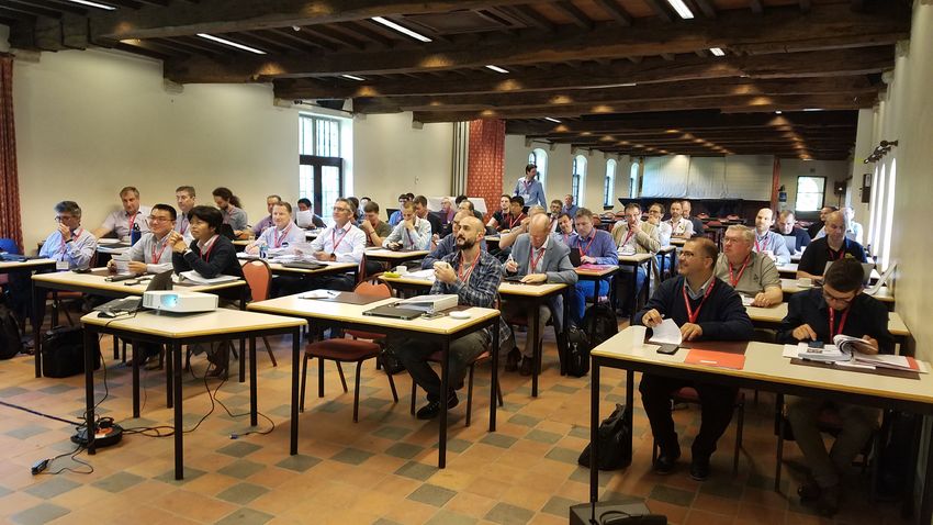
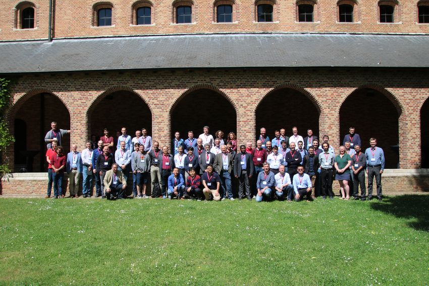
IEW 2018 Turnout Belgium

Management Committee                           Technical Program Committee
Management Committee Chair
Steffen Holland, Nexperia                      Dietmar Walther, Texas Instruments
Technical Program Chair                        Kai Esmark, Infineon
Heinrich Wolf, Fraunhofer EFMT                 Nathan Jack, Intel
Keynote Chair                                  Christian Stockreiter, ams
Theo Smedes, NXP Semiconductors                Evan Grund, Grund Technical Solu-
Invited Speaker and Seminar Co-Chairs:         tions
Shih-Hung Chen, imec                           Stevan G Hunter, ON Semiconduc-
                                               tor
Yiqun Cao, Infineon Technologies AG
                                               Dolphin Abessolo Bidzo, NXP
Discussion Group and Special Interest Group
Chair                                          Rita Fung, Cisco
Fabrice Caignet, LAAS/CNRS                     Andrea Boroni, STMicroelectronics
Audio/Visual Chairs
Vasantha Kumar, Nexperia
Paul Phillips, Phasix
Industry Council Advisor
Harald Gossner, Intel Deutschland GmbH
EOS/ESD Association, Inc. Operations Chair
Christina Earl
EOS/ESD Association, Inc. Director of Events
Nathaniel Peachey, Qorvo
Experience IEW
Greetings from the 14th annual International ESD Workshop (IEW) Management Team! This
event presents a unique opportunity for attendees to participate in in-depth discussions and
learning on EOS and ESD topics in a highly interactive environment. Part of the interactive
environment comes from the event location itself. This event will be held at the Tagungshotel
Jesteburg, Germany.
Located just outside the center of the small town of Jesteburg the meeting hotel is surrounded
by a wood. The quiet surrounding encourages stimulating discussions and immersive
interaction. Focused discussion groups, held in the evenings, are a unique part of our
interactive workshop. While each EOS/ESD topic discussion is facilitated by an expert on the
subject, the main discussion will take place among the participants. The discussion groups
will address topics of the focus issues and include ESD soft failures, challenges for advanced
CMOS ESD protection, System level test for IOT and wearable devices, latch-up, on-chip
health monitoring strategies and the possible impact of reducing CDM limits to 150V.
Scheduled poster sessions are the core of the technical program. These poster sessions
begin with a brief summary of their contribution by each author. These teasers encourage the
participants to visit each poster and its author in the subsequent interactive poster discussion
session. To compliment the offering, attendees are also encouraged to bring open posters.
This format provides an ideal forum for learning and the interchange of new ideas. Topics
covered in the poster sessions include CDM effects and failures, Test cases, ESD verification
with EDA tools, ESD devices for advanced CMOS technology, models for SEED simulations,
on-chip ESD protection devices, latch-up and interconnect investigations.
The IEW also provides a forum for interactive special interest groups (SIGs), on selected
subjects that may extend beyond the IEW time frame. Some SIGs have been successfully
meeting for several years.
A number of stimulating state-of-the-art EOS/ESD seminars, as well as invited talks are
scheduled. Come and listen to presentations, and later meet with the presenters, discussing
ESD protection for brain implantable electronics, FD-SOI technology, fast transients of CDM,
side channel attacks on chips with security functions, Challenges for System Technology
Co-Optimization approach, EMC design and soft failures, electrical overstress and new IEC
testing results.
An afternoon is allocated for recreational activities with fellow attendees, allowing Jesteberg
and its surroundings to be enjoyed, perhaps taking advantage of its proximity to the city of
Hamburg. This is a great way to get to know your EOS/ ESD colleagues better.
Come and meet experts, share your views, ask questions, and extend your network with EOS/
ESD experts from industry and academia. Above all, learn how to efficiently deal with today’s
EOS/ESD challenges and prepare for tomorrow in an informal and interactive atmosphere.
Register for this event early. This will help us in the final planning and preparation for a highly
successful event. We sincerely hope that you will join us in Jesteburg, Germany for the 2020
IEW.

                                                                                              3
Tutorial Monday 2:30 - 4:30 PM
Advanced TLP Applications
Instructor: Heinrich Wolf, Fraunhofer EMFT

The tutorial covers accuracy aspects of transmission line testing and explains how
to do characterization and parameter extraction for compact modelling including
switching behavior and electro-thermal aspects. Furthermore, it discusses SOA
measurements and the application of CC-TLP as a CDM like stress method.
                   Heinrich Wolf received his diploma degree in electrical engi-
                   neering from the Technical University of Munich (TUM) and his
                   PhD from the Technical University of Berlin, Germany. He joined
                   the chair of integrated circuits at TUM as a member of the sci-
                   entific staff working on electrostatic discharge related issues.
                   This involved modeling of ESD-protection elements, parameter
                   extraction techniques, and test chip design. In 1999, he joined
                   the Munich branch of the Fraunhofer Institute for Reliability and
Microintegration (IZM) which became the Fraunhofer Institution for Microsystems
and Solid State Technologies EMFT in 2010. He was involved in the investigation
of ESD protections for CMOS and smart power technologies. Furthermore, he
worked on the simulation and development of ESD protections and on the devel-
opment of ESD test methods and tester characterization. He is also coordinating
the ESD related activities at the EMFT including the development of ESD test
systems and the design of protection structures for deep submicron technologies.
Furthermore, he works in the field of RF simulation and characterization in the
frequency range up to 110 GHz. Currently he also represents the german ESD-Fo-
rum in the standards working groups.

Monday Entertainment 7:30 PM
Keynote
ESD Protection for Medical Implants
Wolfgang Krautschneider, Hamburg University of Technology

Scaling-down of CMOS circuits is accompanied by a huge performance increase of in-
tegrated circuits that opens up much potential of electronics for medical implants. There
are already some electronic implants in use, e.g., pace makers, cochlear implants and
implants for deep brain stimulation. Implants for other medical applications are in an early
state or under development.
Biological signal sources show in most cases a very high impedance and provide sig-
nals with a very low amplitude. This requires amplifiers with very high input impedance
provided by MOS transistors. For handling the electronic circuits during assembly, all the
pads connected to gates of MOS transistors have to be protected by ESD devices that
may degrade the input resistance resulting in worse signal to noise ratios. An appropriate
trade-off has to be found that will be illustrated by demonstrators for medical implants.
Another challenge for medical implants are the very high magnetic fields of MRI which
may generate high voltages that have to be handled by protection structures.
One out of four persons in western countries gets the diagnosis cancer with metastases.
They are treated by systemic therapy (chemotherapy etc.) combined with radiotherapy
applying comparably high radiation doses. When these patients carry medical implants,
the radiation can degrade the characteristics of ESD protection devices, so that design
measures have to be taken to adjust their radiation robustness accordingly.

                         Wolfgang H. Krautschneider (M’85) received the M.Sc., Ph.D., and Habil-
                         itation degrees from the Berlin University of Technology, Berlin, Germa-
                         ny.,He was with Central Research Laboratories, IBM, Yorktown Heights,
                         NY, USA, the Siemens Research Center, Munich, Germany, and the
                         DRAM Project of IBM and Siemens, Essex Junction, VT, USA. He is cur-
                         rently the Head of the Institute of Nanoelectronics at the Hamburg Univer-
                         sity of Technology, Hamburg, Germany.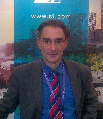
Invited Talks
Invited Speaker Co-Chairs:
Shih-Hung Chen, imec
Yiqun Cao, Infineon Technologies AG

Invited talks always give good opportunities to broaden workshop attendees’ exposure to expertise in different fo-
cused areas of interests. This year, three invited talks are included with wide-range aspects from process technol-
ogy, chip security, to system qualification. The talk from Dr. Philippe Galy, STMicroelectronics, is one of the focus
topics of this year. It is dedicated on ESD/LU challenges for ultra-thin body and box (UTBB) fully depleted SOI (FD
SOI) CMOS technology for 2D and 3D innovative solutions. Dr. Galy will give an introduction of this UTBB FD SOI
technology and will also discuss innovative ESD solutions. The talk from Alexander Schlösser, NXP, will focus on
side channel attacks for high security automotive chips. In this talk, Alexander will look at how hardware security
analysis uses soft failures and will explore the differences and similarities to ESD-related failures. The talk from
Dimitri Linten, imec, will focus on the scaling technology with system technology co-optimization (STCO) approach
toward node N5 and beyond. Dr. Linten will give an introduction of the novel STCO approach and will discuss the
ESD reliability challenges in this technology.

Invited Talk 1
UTBB FD-SOI and ESD/Latch-up: Challenges and Solutions
Philippe Galy, STMicroelectronics
This talk is dedicated to ESD/LU challenges for Fully Depleted SOI (FD-SOI) Ultra Thin Body and Box (UTBB)
CMOS technology nodes for 2D and 3D innovative solutions. After an introduction on the UTBB FD_SOI technol-
ogy provided by STmicrolectronics, especially in 28nm High k metal gate, the ESD protection challenges in this
technology will be discussed along with solutions. Preliminary silicon results with 2D/3D innovative solutions are
introduced according to performance and integration. Moreover, radiation effects are also addressed.

                    Philippe Galy born 1965, received the Ph.D. from University of Bordeaux and H.D.R from
                    LAAS CNRS University of Toulouse. He is a fellow, technical director at STmicrolectronics
                    Research and Development France. He has proposed a full CDM protection and several
                    new ESD compact devices for mature & advanced CMOS technologies. He supports sev-
                    eral teams for research focused on new innovative solutions: Memory + silicon Qubit and
                    cryo-design, Neuromorphic, 3D ultimate integration. He has authored or coauthored several
                    publications (+100), books (3), and patents (+100). He serves in TPC and is a reviewer for
                    many symposiums and journals. He is also involved in National (3) and European projects (4).
                    Also he joins the QuEng CDP team from Grenoble and also adjunct professor at “ Université
                    de Sherbrooke (UdS)”.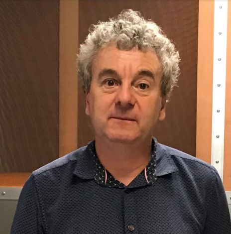
Invited Talk 2
Reliability Challenges in Scaling Era with System Technology Co-Optimization
(STCO) Approach
Dimitri Linten, imec
From the 10 nm technology generation onward, traditional scaling has been complemented by design-technology
co-optimization (DTCO), combining expertise from technology as well as from design. But, as the technology mov-
ing forward, the benefits of DTCO in system-on-chip (SoC) applications are expected a certain saturation. For 3 nm
and beyond technology nodes, the focus will shift from scaling at logic cell level towards scaling at system level.
Hence, DTCO is evolving into an system technology co-optimization (STCO)-oriented approach. More and more
(sub-)system functions will be integrated in one chip with a special 3D vertically stacked or 2.5D interposer architec-
ture. However, a chip-level or even a system-level electrical reliability becomes necessary to evaluate at the early
stage of the technology/circuit/system development period.
In this talk, we will look at the technology features of the STCO approach, including different 3D integration technol-
ogies applied in different levels of interconnect hierarchy. In addition, the emerging reliability challenges will be also
discussed from different aspects in the STCO framework. .
                        Dimitri Linten received PhD degrees in electrical engineering from the Vrije Universi-
                        teit Brussel (VUB), Brussels, Belgium in 2006. Since 2015, he is the R&D manager
                        of the Device Reliability and Electrical characterization group at imec. He is a senior
                        member of the IEEE (SM13). His main research interests are ESD reliability, Mem-
                        ory and logic device reliability physics, radiation, biosensors and security. He has
                        served as a technical program committee member of several international scientific
                        conferences, among which the International Reliability Physics Symposium (IRPS),
                        the EOS/ESD Symposium, the International ESD Workshop (IEW) and International
                        Electron Devices Meeting (IEDM).

Invited Talk 3
Soft Fails as a Tool in Hardware Security Analysis
Alexander Schlösser, NXP Semiconductors
While soft fails are to be avoided from an ESD point of view they can be quite useful in another domain. Hardware
Security Analysis is a specific field in the wide world of hacking and penetration testing. It focuses largely on so-
called implementation attacks, targeting the unintended imperfections and compromises in the physical realization
of a digital design. The methods for these attacks are often derived from failure analysis and include the use of
lasers, micro- and nano-probes as well as small-scale antennas and field generators.
A specific group of methods are Fault Injection Attacks. These are active but non-invasive efforts to intentionally
cause soft fails, with the aim to compromise the secure handling of to-be-protected data. This talk will introduce the
systems and methods used in fault injection attacks and the physical effects and interactions that are exploited. It
will show how hardware security analysis uses these fails and discuss differences and similarities to ESD-related
fails.

                       Alexander Schlösser is a Senior Security Analyst with NXP Semiconductors. As a member
                       of NXP’s internal hacking team he conducts hardware security analyses of Smart Cards
                       and Secure Elements as well as automotive and application processors. Alexander has a
                       background in photonics and received a PhD in physics from TU Berlin before he joined
                       NXP in 2014. Since then he develops systems and methods to identify and root-cause vul-
                       nerabilities and weaknesses in digital designs with a security focus.

                                                                                                                   7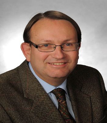
Seminars
Seminar Co-Chairs:
Shih-Hung Chen, imec
Yiqun Cao, Infineon Technologies AG

Four recognized experts from university, research institute, and industry will give seminar talks on some of the
highly interesting topics at this year’s IEW. These seminar talks are covered with the main ESD challenges in
system-level, component-level, and even manufacturing perspectives. The seminar from Dr. Wolfgang Stadler,
Intel, will focus on non-standard overstress in manufacturing phase and will show the (mis)correlation between
IC ESD qualification waveforms and real world risks in handling ICs, boards, and systems. The seminar from
Professor David Pommerenke, ESDEMC, will focus on system-level ESD testing and will discuss the reasons
for large uncertainty of the test results even when carefully following the procedures in IEC 61000-4-2, as well
as give suggestions to the test implementation. The seminar from Professor Franco Fiori, Politecnico di Torino,
will focus on circuit-level EMC/EMI design and will discuss recent progresses on the EMI immune designs of
MEMS readout circuits. Finally, the seminar from Johannes Weber, Fraunhofer EMFT, will focus on fast transient
of CDM ESD event and will cover wide-range perspectives of the fast rise time (or fast slew rate) from the fun-
damental theory to the testing methodologies.

Seminar 1                                                                         Dr. David Pommerenke received
                                                                                  his diploma and PhD from the
Achieving Meaningful and Repeatable Re-                                           Technical University Berlin,
sults in ESD System Level Testing                                                 Germany. His research interests
                                                                                  are system level ESD, electronics,
David Pommerenke, Technical University of Graz.
                                                                                  numerical simulations, EMC
The vast majority of system level ESD testing follows the                         measurement methods and
specifications defined in IEC 61000-4-2. Unfortunate-          instrumentation. He worked at Hewlett Packard
ly, even when carefully following the procedures in IEC        for 5 years before joining the electromagnetic
61000-4-2 there is a high level of uncertainty in the test     compatibility laboratory at the Missouri University
results, and successful passing of the test requirements is    of S&T in 2001. Dr. Pommerenke became the CTO
often not a good prediction of ESD robustness in the field.    of ESDEMC in July 2019 before joining the ESD/
The talk, which is based on a white paper by the Industry      EMC group at the Technical University of Graz in
Council on ESD Target Levels explains deficiencies of the      Austria in January 2020. His new focus is on ESD,
standard and problems within the generally applied test        EMC, harmonics, and PIM. He has published more
procedures. Based on this analysis the talk suggests im-       than 200 papers and is inventor on 13 patents.
provements to both the standard, and the test implemen-        His main research interests are measurement/
tation.                                                        instrumentation ESD, electronic design and EMC.
This includes                                                  He is IEEE fellow and associated editor for the IEEE
 - better ESD gun specifications                               Transactions on EMC.
 - Full wave and SPICE models for ESD generators
 - Simulation of ESD robustness following the SEED con-
cept (System Efficient ESD Design)
 - Improved documentation, such as measuring the ESD
current during testing
  - Improved test produced e.g., number of discharges,
methods of stabilizing the arc in air discharge etc.
 - Robotic ESD testing
The goal of the talk is to explain the reasons for the large
test result uncertainty, to give suggestions to the standard
committee for improvements and to enable engineers to
implement the test in such a way that results are mean-
ingful, repeat well and give indications for the root cause
of a failure.
Seminar 2                                                        Seminar 3
Correlation of Qualification ESD Robust- Recent Advances on the Design of
ness and Handling Threats                MEMS Readout Circuits Immune to
Wolfgang Stadler, Intel Deutschland GmbH EMI
                                                                 Franco Fiori, Politecnico di Torino
Today, almost all integrated circuits (ICs) are qualified with
respect to Human Body Model (HBM) and Charged Device             Among the circuit topologies available in the open
Model (CDM). Current international standards on ESD Con-         literature for the design of MEMS readout circuits,
trol Programs require a minimum ESD robustness of 100 V          those based on the current feedback differential
according to HBM and 200 V of CDM for ICs to ensure safe         difference amplifier (DDA) are usually preferred
handling. However, there is no clear correlation between         because they feature a wider differential input
qualification waveforms and waveforms of reel ESD events         range (DMIR), rail-to-rail common mode input
even on IC level, therefore, the qualification might not nec-    range (CMIR), high power supply rejection (PSR)
essarily cover all problems.                                     as well as high noise figure. These are valuable
The situation is even worse if ESD events on system lev-         features for low voltage applications. In addition,
el are considered. Such events mainly occur during board         such a topology lends itself well to implement aux-
and system assembly or during testing, like Charged Board        iliary circuits such as those needed for input bias-
Events, Cable Discharge Events, or transient latch-up. To-       ing or DC offset cancellation or AC calibration.
day, there are no widely accepted ESD qualification stan-
dards on most of these ESD system level events, this is
one reason why the ESD control standards refer to IC level                        Franco Fiori(M’02) received the
robustness only.                                                                  Laurea and Ph.D. degrees in
In this presentation, we will assess the (mis)correlation be-                     electronic engineering from the
tween IC ESD qualification waveforms and real world risks                         Polytechnic University of Turin,
in handling ICs, boards, and systems. We will also discuss                        Turin, Italy, in 1993 and 1997,re-
which ESD system level characterization methods could                             spectively. From 1997 to 1998,
help to improve the ESD process assessment methodolo-                             he was an R&D Leader ofST-
gies of boards or system handling processes.                                      Microelectronics, Milan, Italy. In
                                                                                  1999, he joined the Electronics
                                                                 and Telecommunication Department, Polytech-
                    Wolfgang      Stadler    received    his
                                                                 nic University of Turin, where he is currently an
                    diploma degree in physics in 1991
                                                                 Associate Professor of Electronics. From 2006 to
                    and in 1995 the PhD degree from the
                                                                 2010, he was the Scientific Leader of a joint ST-
                    Physics Department of the Technical
                                                                 Microelectronics-Politecnico di Torino Research
                    University Munich. 1995 he joined the
                                                                 Laboratory aimed to investigate chip-level EMC
                    semiconductor division of Siemens,
                                                                 issues. He has authored and coauthored more
                    which became Infineon Technologies
                                                                 than 170 papers published in international jour-
                    in 1999. His focus was on development
                                                                 nals and conference proceedings. His research
                    of ESD-protection concepts in CMOS
                                                                 interests include analog circuit design, mac-
technologies and on innovative ESD topics. In this role he       ro-modeling of active nonlinear circuits, smart
was coordinator of several European and German ESD               power devices, and electromagnetic compatibil-
funding projects. Since 2003, he was also been responsible       ity.
for the measurement characterization of I/O cells and PHYs.
In 2011, he joined Intel Mobile Communications which is
now Intel Deutschland GmbH. Within the corporate quality
network, he is currently responsible for the ESD control
program of Intel and for ESD risk assessment. Furthermore,
he supports ESD/latch-up testing and qualification of
products. Wolfgang holds several patents in ESD-related
topics. He is author or co-author of more than 120 technical
papers and has co-authored a book on ESD simulation.
He has received several best paper awards and teaches
courses on ESD device testing, ESD qualification, and
ESD control measures (for example, TR53 ESD Technician
Certification).
Seminar 4
Stress Current Rise Time Evaluation in
the Single-Digit Picosecond-Domain
Johannes Weber, Fraunhofer EMFT
This talk will cover ESD behavior of carbon nano
tubes as well as Graphene devices. Unique shell by
shell breakdown of CNTs under ESD stress condition
and dependence of current transport on the nature of
CNT will be discussed. The role of contacts will be
presented. In context of CNT interconnects, ESD
behavior of multi-wall CNT bundles will be presented
too. In the second half, the talk will cover ESD
behavior and physics of carrier transport at ESD time
scales through graphene transistors. The impact of
technology parameters on ESD behavior and failure
current will be presented. The role of contacts and
evidence of heat propagation through contacts will
be presented through details Raman spectroscopy
measurements. Finally, record high failure current and
a unique defect assisted failure of graphene FETs will
be disclosed.

                    Johannes Weber received his
                    Master’s degree in physics from
                    the Technical University Munich
                    (TUM) in 2015. He wrote his
                    Master’s thesis in the research
                    area of Nuclear, Particle and
                    Astrophysics at the Max Planck
                    Institute for Extraterrestrial Physics
                    (MPE). Afterward, he joined the
                    Team of Analysis & Test at the
Fraunhofer Research Institution for Microsystems and
Solid State Technologies EMFT in Munich, Germany
as a research associate. He works in the field of
Electrostatic Discharges (ESD) and focuses on the
development of ESD test methods and ultra-fast ESD
events in the picosecond domain. His research mainly
deals with the influences of critical stress parameters
like the rise time or the energy content of the stress
pulse on the failure level of advanced semiconductor
technologies. Supported by the ERC Grant 2016 of the
ESD-Association, he finished his PhD thesis with the
title “Pulsed High Current Characterization of Highly
Integrated Circuits and Systems” at the Bundes-wehr
University of Munich in 2019.
Discussion Groups
Discussion Groups Chair:
Fabrice Caignet, LAAS/CNRS
The discussion groups are an integral part of the workshop. There will be six discussion groups offered,
with three parallel sessions on Tuesday evening and three parallel sessions on Wednesday evening. The
topics include ESD soft failures; ESD challenges for advanced CMOS (FD-SOI, beyond FINFETS); discus-
sions on health monitoring, the appropriateness of system level testing for IoT devices/wearables; latch-
up; and testing devices for CDM below 150 volts. Each discussion group has a moderator with extensive
expertise on the topic to help guide and inspire the discussion. The success of these sessions depends on
your active participation. We encourage you to bring along data, ideas, and other items of interest to share.
Session A
Parallel Groups-Tuesday 7:00-8:30 PM
DG A.1 DG A.2
ESD Challenges for Advanced CMOS (FD-SOI, System Level Test: is it Appropriate for IOT
Beyond FINFETS) Devices/Wearables?
Co-Moderators: Shih Hung Chen, imec; Philippe Galy, Co-Moderators: Adrijan Barić, University of Zagreb
STMicroelectronics Faculty of Electrical Engineering and Computing; Har-
ald Gossner, Intel Deutschland GmbH
While Bulk FinFET and Fully-Depleted (FD) SOI
technologies have become the mainstream in the ad- System level testing using IEC 61000-4-2 is like an
vanced CMOS IC industry, what are the next technol- elephant in a glass shop; it seems to be widely ap-
ogy options or next device architectures after FinFET plicable and it produces sound results. However,
and FD SOI? Several promising candidates have the question is, is it really useful and relevant for
been proposed; however, only very few prior works real world events or is there any better approach?
discussed ESD reliability in these promising future Also, what are the most appropriate test levels for
technologies. In addition, the challenges might not tiny IoT devices. Are the size of the IoT device and
only from technology options but also from more real- the technology node critical for the energy that can
istic aspects, such as design verification and product be dissipated on the device? What are the ulti-
qualification. This discussion group aims to look at mate sustainable testing levels for the down scaled
the ESD challenges in advanced CMOS technologies technology nodes that will inevitably penetrate into
with varied perspectives. With your ideas and sharing the IoT market? Finally, when we do system level
experience, this discussion group will be able to bring testing, do we look only for the functionality of the
some clarity to those emerging ESD challenges. device or we also have to worry about safety of
the system. Is it possible to disturb the operation in
such a way that the data sent from IoT device can
generate a twisted image of the reality?DG A.3 Is Latch-up Testing Still Relevant? Moderator: Guido Quax, NXP Semiconductors The category of low voltage IC products has ex- perienced an ever decreasing operating voltage, such that a setup according to the latchup stan- dard (JEDEC78E) does not lead to any current injection stress. On the other hand, the number of products with a severe system level stress re- quirement (like IEC61000-4-2 or IEC61000-4-5) is increasing. The risk for ‘soft failures’ (latchup) would, in this case, not be covered by passing the JEDEC78E test. This leads to a question: does the standard need to get better ‘aligned’ with the modern product portfolio? And if so, how should that be done? One can think of product categories, each with their own stress. How should the reference stress for a product category be determined? Next to these possible improvements to the standard, we would like to reflect with you on the cause of current in- jection stresses in ‘the real world’. In which situa- tions do you think the +/- 100 mA stress could still occur, and are there actual field returns related to situations beyond this current stress level? How can the standard capture these situations? With this discussion we aim to get a better insight in the limitations of the current JEDEC78E standard.
Session B
Parallel Groups- Wednesday 7:00-8:30 PM
DG B.1                                                       DG B.3
ESD Induced Soft Failures                                    Testing Devices for CDM Below 150 Volts
Moderator: David Pommerenke, ESDEMC                          Moderator: Marko Simicic, imec

This discussion group will try to answer the root cause      The CDM device testing levels are dropping be-
of soft-failures, methods for modeling, and counter-         low 150 volts. One of the reasons for that is the
measures. The root-cause includes, the discharge,            technology advancement. However, the zap-to-
the system level coupling path, and the internal rea-        zap variability of the standard Field-Induced CDM
sons of the IC which lead to a soft-failure. Modeling of     (FI-CDM) tester used today drops significantly for
soft-failures can be successful using circuit informa-       low voltages. Alternative CDM testers such as
tion if the region inside the IC is well defined. Howev-     the capacitively-coupled TLP or the low-imped-
er, in most cases behavioral models will be needed.          ance contact CDM (LICCDM) do not have issues
Here behavioral models for USB 3.x will be presented         with variability. However, their relay-based testing
and compared to measurements. A variety of counter-          mechanism is significantly different to the current
measures exist, obviously in software, but it is also        standard. In this discussion group, we will discuss
possible to use TVS diodes such that they not only           questions as:
prevent damage, but reduce soft failures strongly.
This will be explained based on a USB 3.x example to         What are the reasons for lowering the CDM test-
start an open discussion on all aspects of soft failures.    ing level?
                                                             Is the pulse rise time an issue for LICCDM/CC-
DG B.2                                                       TLP?
Health Monitoring: Can we use Transient
Event Detection of EOS/ESD to Build More                     What are the concerns with testing CDM on
                                                             non-packaged dies and wafers?
Resilient Systems?
Moderatos: Franz Dietz, Henning Lohmeyer, Robert             Should we be reporting the CDM currents instead
Bosch GmbH; Patrice Besse, NXP Semiconductors                of the voltages?

Over the last years there has been significant atten-
tion within reliability engineering to the so called third
generation of reliability. Such resilient systems are
designed to be aware of their health status by rec-
ognition of critical stress-strength combinations. This
enables the system to react to changed situations or
even to compensate errors prior to failure. On a hard-
ware level it is proposed to introduce detectors for
aging, mission profile logging and impeding failure of
SoC. Additionally, detectors for events exceeding nor-
mal operation region were proposed which arguable
could include EOS/ESD. Specifically for ESD threads,
transient event detectors have been discussed that
monitor exposure of the systems to ESD-stress during
assembly and field usage. Furthermore such detec-
tors have been proposed to support analysis of ESD
soft failures and enable containment of such events
on system-level. By sorting through the different ap-
proaches and targets of implementing transient event
detectors, the discussion group aims to identify the
potential benefits and limits of such an approach in the
context of resilient systems for different applications.
What can we learn from detecting and even measur-
ing strength of ESD/EOS events in assembly and field
and how do we use such information for more resilient
and safe systems?
Technical Sessions
Technical Session Chair: Heinrich Wolf, Fraunhofer EFMT
This year’s IEW technical program consists of three sessions, where peer-reviewed poster presentations
are discussed together with the authors and interested colleagues. The authors will introduce their work in
a short podium “teaser” presentation before the extended interactive discussion with the workshop partici-
pants at the poster sessions. This format allows an in-depth exchange of ideas among a diverse audience in
a very informal setting. A wide variety of ESD subjects will be covered, including ESD simulation/verification
of full chips and single elements, system related and general measurements aspects and device physics
covering the behavior of single elements, and also latch-up.
Technical Session A: Simulation Related Topics
A.1 CDM Failures at Internal Nodes— Challeng- A.4 Chip-Level ESD Verification Using
es for Future CDM Simulation and Understand- Graph-Theory Based Approach
ing of Test Results Vlatko Galić, Adrijan Barić, University of Zagreb;
James Karp, Xilinx, Inc. Aarnout Wieers, Renaud Gillon, ON Semiconductor
This poster will share case studies of CDM failures A new Electrostatic Discharge (ESD) verification
observed at internal nodes 100 microns away from flow is proposed. The presented methodology uses
I/O pads. The author will propose a device physics piecewise linear models based on transmission line
model that explains CDM failures that cannot be pulsing (TLP) measurements to ascertain the level
characterized with VFTLP and simulated with avail- of ESD robustness of integrated circuits (IC) and
able current density tools. to detect ESD current paths. This flow is based on
graph-theory Floyd-Warshall algorithm.
A.2 X-FAB ESD Design Checker an Automated
Tool for Full Chip ESD Simulation A.5 Full-Chip CDM Analysis: Is Static Simulation
Enough?
Vadim Kuznetsov, X-FAB Dresden GmbH & Co.
KG; Lars Bergmann, X-FAB Global Services GmbH Jordan Davis, Chanhee Jeon, Sung-Jun Song,
Samsung Electronics; Yuri Feinburg, Simon Young,
Silicon Frontline
X-FAB ESD Design Checker (XESDC) is the tool for
full chip ESD analysis. It performs a virtual TLP test
and finds ESD weaknesses of IC design using the To improve understanding and verification of ICs be-
CDL or SPICE extracted netlist and technology-spe- fore manufacturing, a static approach to CDM verifica-
cific ESD model library. XESDC works independent- tion and analysis is explored. In the absence of full-chip
ly from EDA platforms using the built-in simulation transient circuit simulation, considered computationally
core. prohibitive, enhancements to the static approach have
been made. These enhancements are able to find po-
tential failures regardless of technology or design.
A.3 ESD Charaterization and TCAD Simulation of
Reversed ggNMOS in Advanced Bulk FinFET Tech-
nology
W-C. Chen, S-H. Chen, G. Hellings, Y-K. Siew, J. Chen,
G. Groeseneken, D. Linten, imec
In this work, the ESD performance of reversed GG-
NMOS in the advanced bulk FinFET are investigat-
ed. The impact of the layout parameters, such as
gate length (Lg) and the distance of the gate and
the drain contact (Lgd) are demonstrated by the TLP
measurement and studied by the 3D TCAD simula-
tion.Technical Sessions continued
Technical Session B: System-Level and General Testing Aspects
B.1 Display Driver IC`s System Level ESD Fail- B.4 A Discussion on ESD Data in IC Datasheets
ure Case Study with Component Level ESD Test Bart Huitsing, Theo Smedes, NXP Semiconductors
& Analysis
Sung-Joon Song, Young-Min Kim, Chang-Su Kim, Despite the publication of a Standard Practice and
Chan-Hee Jeon, Samsung Electronics Co., Ltd consolidated Joint ESD Standards, it remains chal-
lenging to specify a correct and exhaustive ESD ro-
A display driver IC’s EOS/ESD failure case observed bustness of application specific components. We will
in TV assembly line. The root cause of IC failures is discuss suggestions how to deal with e.g. IC’s with
identified to be the gate oxide rupture. In this case mixed pin specific robustness requirements or IC’s
study, the effectiveness of the resistance analysis tool with non-standard pin-to-pin discharge requirements.
is demonstrated through the component level ESD test
to identify the IC failure. B.5 Influence of Parasitic Impedances on LI-
CCDM Testers
B.2 Generalization of Modelling Concept for Marko Simicic, Wei-Min Wu, Shih-Hung Chen, Dim-
Common Mode Choke (CMC) itri Linten, imec; Shinichi Tamura, Yohei Shimada,
Sergej Bub, Nexperia Germany GmbH Masanori Sawada, Hanwa Electronic Ind. Co., Ltd.
In this poster, a generalized modeling concept for It is expected that CDM testing on wafer level and
Common Mode Choke (CMC) is presented. The with pre-charge voltages below 150 V will soon be-
S-Parameters based small-signal model of CMC is come necessary for new technologies. Low-Imped-
extended with dynamic and saturation working re- ance Contact CDM (LICCDM) is one of the candi-
gions evaluated using the Transmission Line Pulse dates that could satisfy these requirements. In this
(TLP) test method. The developed CMC model is work we study the parasitic impedances that affect
verified on the different types of CMC. the LICCDM tester.
B.3 Using Fast Transient Characterization (FTC) B.6 De-Embedding of VF-TLP/CC-TLP Systems
for EOS Risk Mitigation Johannes Weber, Ellen Jirutková, Heinrich Wolf,
Dietmar Walther, Raj Sankaralingam, Texas Instru- Horst Gieser, Fraunhofer EMFT
ments
This poster presents a De-/Embedding technique for
The introduced method applies fast transient pulses TDR-based test methods like VF-TLP or CC-TLP. It
(residual IEC 61000-4-2 pulses) with high energy to replaces the manual determination of the time shift
a powered device. parameter between the incident and reflected pulse
Besides soft failures also electrical induced physical by fully reconstructing the signals at the DUT con-
damages (EIPD) are observed which were undetect- sidering dispersion effects. Instead of S-parameters
ed during HBM/CDM. of the test fixture which should be de-embedded, its
Once fails are identified, simulation is used identi- calibration requires only three pulses in time domain.
fying circuit weaknesses to comprehend powered
ESD fail modes.
15Technical Sessions continued
Technical Session C: Device Physics and Design
C.1 Evaluating Latchup (LU) Risk in Advanced C.4 Influencing SCR Holding Current by
CMOS Technologies Segmentation Topology
Guido Groeseneken, Kateryna Serbulova, KULeu- Vasantha Kumar, Steffen Holland, Hans-Martin
ven ESAT, imec; Shih-Hung Chen, Geert Hellings; Ritter, Nexperia
imec
A segmented layout topology on a novel SCR is
In advanced CMOS technologies, LU risk becomes used to obtain a higher holding current (Ihold).
one of the major reliability concerns because of the The SCR Ihold has been increased by reducing the
shrinking layout dimensions. LU originates from par- emitter area of the PNP, which reduces the injection
asitic BJTs forming SCR path. The beta gain of these efficiency of the PNP. The increased ability to collect
parasitic BJTs is essential characteristic for LU preven- free carries results in higher Ihold.
tion that is evaluated for different layout configurations
in this work.
C.5 Interconnect Capacitance Investigation
C.2 Single Event Latchup or Multi Event Latch- and Optimization Under I/O Pad for ESD Pro-
up - How Far Can You Push it? tection of RF/High-Speed Circuits in Micro-&
Nano-scale CMOS Technology
Geert Hellings, Brecht Truijen, Marko Simicic, Shih-
Wei-Min Wu, imec; NCTU; KU Leuven, Shih-Hung
Hung Chen, imec
Chen, Dimitri Linten, imec; Guido Groesenek-
en,imec-Leuven; KU Leuven
During SEL robustness tests, a chip is exposed to a
high flux of radiation. We investigated the probability
of Multi Event Latchup (MEL) during such acceler- Recently, new distributed network to put ESD devic-
ated tests. Based on TCAD and theoretical deriva- es under I/O pad was proposed. However, parasitic
tions, we find that MEL can occur, although it highly capacitance gets more critical to RF degradation. In
depends on the test specifics (# of DUT, test flux, this work, investigation of capacitance, technique of
layout, etc.). BEOL capacitance reduction, S-parameter and TLP
measurement, and optimization between RF and
ESD are compared, fabricated, and proposed.
C.3 Triggering of Multi-Finger and Multi-Seg-
ment SCRs Near the Holding Voltage Studied by C.6 Effects of Current Density and Geometry on
Emission Microscopy Under DC Conditions Parasitic NPN Transistors in CMOS
Hasan Karaca, Dionyz Pogany, TU Wien; Clement Guido Quax, NXP Semiconductors
Fleury, CTR Carinthian Tech Research AG; Stef-
fen Holland, Hans-Martin Ritter, Guido Notermans,
Nexperia This work investigates the behavior of parasitic npn
bipolars in an advanced CMOS and a submicron
power technology as a function of current injection
Emission microscopy under DC current controlled level and multiple geometric parameters. We intend
mode has been used to study current flow distribu-
tion in multi-finger and multi-segment SCRs. The el- to create an integral empirical model, which can be
ements trigger at nearly the same current density in- easily applied during the design practice.
dicating the substrate-coupled triggering mechanism
found previously under TLP regime. On-resistance
and holding current aspects are also discussed.
start
12:00 14:30
            end         Monday
                        Optional Lunch
                                                             Schedule
13:00 16:00             Registration
14:00 14:30             Free Time
14:30 16:30             Tutorial: Advanced TLP Applications
		                      Heinrich Wolf, Fraunhofer EMFT
16:30 17:00             Break
17:00 18:00             Seminar 1: Achieving Meaningful and Repeatable Results
		                      in ESD System Level Testing
		                      David Pommerenke, ESDEMC
18:00 19:30             Dinner
19:30 20:30             Welcome entertainment
20:30 21:30             Networking/ Social Gathering

start       end         Tuesday
7:30   9:00 Breakfast
9:00   9:30 Welcome (open poster question)
9:30  10:30 Keynote: ESD Protection for Medical Implants
		          Wolfgang Krautschneider, Hamburg University of
		Technology
10:30 11:00 Break
11:00 12:00 Invited talk 1: UTBB FD-SOI and ESD/Latch-up:
		          Challenges and Solutions
		          Philippe Galy, STMicroelectronics
12:00 13:00 Lunch
13:00 14:00 Seminar 2: Correlation of Qualification ESD Robustness and
		          Handling Threats
		          Wolfgang Stadler, Intel Deutschland GmbH
14:00 15:00 Technical session A: Simulation Related Topics
15:00 16:30 Poster discussion session A
16:30 17:00 Break
17:00 18:00 Invited talk 2: Reliability Challenges in Scaling Era with
		          System Technology Co-Optimization (STCO) Approach
		          Dimitri Linten, imec
18:00 19:00 Dinner
19:00 20:30 Discussion Group Session A
		          A.1 ESD Challenges for Advanced CMOS
		          (FD-SOI, Beyond FINFETS)
		          Co-Moderators: Shih Hung Chen, imec; Philippe Galy,
		STMicroelectronics

		 A.2 System Level Test: is it Appropriate for IOT Devices/
		Wearables?
   Co-Moderators: Adrijan Barić, University of Zagreb
		 Faculty of Electrical Engineering and Computing;
		 Harald Gossner, Intel Deutschland GmbH

		                      A.3 Is Latch-up Testing Still Relevant?
		                      Moderator: Guido Quax, NXP Semiconductors

20:30       21:30       Networking/ Social Gathering
start
7:30
end
9:00
Wednesday
Breakfast
Schedule continued
9:00 9:10 Announcements
9:10 10:10 Seminar 3: Recent Advances on the Design of MEMS
Readout Circuits Immune to EMI
Franco Fiori, Politecnico di Torino
10:10 10:30 Break
10:30 11:30 Invited talk 3: Soft Fails as a Tool in Hardware Security Analysis
Alexander Schlösser, NXP Semiconductors
11:30 12:10 Report on DG Session A
12:10 13:30 Lunch
13:30 18:00 Open Time
18:00 19:00 Dinner
19:00 20:30 Discussion Group Session B
B.1 ESD Induced Soft Failures
Moderator: David Pommerenke, ESDEMC
B.2 Health monitoring: Can we use Transient Event Detection
of EOS/ESD to Build More Resilient Systems?
Co-Moderators: Franz Dietz, Henning Lohmeyer,
Robert Bosch GmbH; Patrice Besse, NXP Semiconductors
B.3 Testing Devices for CDM Below 150 Volts
Moderator: Marko Simicic, imec
20:30 21:30 Networking/ Social Gathering
start end Thursday
7:30 9:00 Breakfast
9:00 9:10 Announcements
9:10 10:10 Seminar 4: Stress Current Rise Time Evaluation in the
Single-Digit Picosecond-Domain
Johannes Weber, Fraunhofer EMFT
10:10 10:30 Break/Picture
10:30 11:10 Report on DG Session B
11:10 12:00 Technical Session B: System-Level and General Testing Aspects
12:00 13:00 Lunch
13:00 14:20 Poster Discussion Session B
14:20 14:50 Break
14:50 15:50 Technical Session C: Device Physics and Design
15:50 17:15 Poster Discussion Session C
17:15 17:45 Industry Council Report
17:45 18:00 Closing
18:00 19:00 Dinner
19:00 20:00 Hosted reception
start end Friday
7:30 9:00 Breakfast
9:00 11:00 Check Out
TRAVEL ARRANGEMENTS & ACCOMMODATION
 IEW ACCOMMODATION:
 The IEW will take place in a meeting hotel in Jesteburg, Germany. Jesteburg with a first record in 1202 is located just south of Hamburg,
 in the middle of a wood. In the morning you only hear the rustling of leaves and the bird chirps in the trees. On the first floor there are
 standard rooms, each equipped with private bathroom facilities, telephone and internet access.
 The physical isolation of the location and the absence of distractions encourage extensive interaction among the workshop attendees.
 Lodging and all meals are included in the registration costs for the workshop.
 ● Arrangements can be made for those with special dietary or physical requirements. Please send your re¬quirements with your reg-
 istration or call +1 315-339-6937.

 GUESTS AND SPOUSES:
 You are welcome to bring a guest to IEW. Double rooms are available for spouses and guests in the same room for 20 Euro per night,
 which includes breakfast. Lunch and dinner is offered for an additional cost of 18 Euros and 14 Euros, respectively. Guest fees will
 be charged separately and must be paid directly to the hotel. Attendees must list guests with their initial registration to allow for room
 arrangements as the number of double rooms are limited

 RESPONSIBILITIES OF ATTENDEES:
 Please come prepared to participate actively in the discussions and meetings by sharing your experiences, concerns, questions, views,
 technical information, and test data, as appropriate. Your active involvement in the formal, as well as in the informal meetings and ac-
 tivities, is the key ingredient for maximizing the value of the workshop for you and your fellow attendees. Enjoy IEW!
 In keeping with the relaxed and informal atmosphere of the Workshop, we ask that attendees not overtly solicit, promote, or attempt
 to sell a commercial product or service at the Tagungshotel Jesteburg. On the other hand, we strongly encourage making business
 acquaintances and arranging meetings to be held after the workshop.

 SURROUNDING AREA:
 The meeting hotel is located within walking distance of the center of Jesteburg. The surrounding invites for walks inside the wood. The
 city of Hamburg is located 30km away. It can easily reached by car and public transport in about 40 minutes.
 The city of Hamburg, with 1.8 Mio inhabitants is the second largest city in Germany. It offers a wide range of cultural experiences, from
 art museums, concert halls to the “Miniatur Wunderland”, the world largest model railroad exhibition. You can visit the second largest
 port in Europe by boat as well as the old storage district, the Speicherstadt, which became a UNESCO world heritage in 2015. You can
 also make a trip on the lake Alster in the city center or explore the various channels which pass through the city.
 Enjoy your “Free time” and explore the Hansestadt Hamburg!

 Tagungshotel Jesteburg
 Itzenbütteler Str. 35
 21266 Jesteburg
 GERMANY
 Telephone: +49 4183 93 90
 Fax: +49 4183 93 91 00
 E-Mail: info@tagungshotel-jesteburg.de
 Internet: http://www.tagungshotel-jesteburg.de

 The Tagungshotel Jesteburg is located about 30km from the city center of Hamburg and 50 km from the International Airport of Ham-
 burg (HAM).
 From the airport

 Public transport:
 There are subways to the main train station (Hamburg Hbf) every 10 minutes. From here, a regional train (RE4) to Bremen and stop-
 ping at Buchholz is going ever hour. A bus or a taxi takes you to the Tagungshotel Jesteburg.
 For further information please visit: https://www.hvv.de/en
 The travel takes about 1 hour 20 minutes.
 By Car:
 The travel from the airport takes about 1 hour by rental car.
 From the main train station (Hamburg Hbf)

 Public transport:
 a regional train (RE4) to Bremen and stopping at Buchholz is going ever hour. A bus or a taxi takes you to the Tagungshotel Jesteburg.
 For further information visit: https://www.hvv.de/en
 The travel takes about 45 minutes.
 By Car:
 The travel from the main train station (Hamburg Hbf) takes about 40 hour by rental car.
SIGHTSEEING TIPS FOR HAMBURG
1. Hamburg Parliament/City Hall
2. Speicherstadt
3. Miniatur Wunderland
4. ElbPhilharmonie
5. St. Michael‘s Church
6. Landungsbrücken Piers and Old Elbe tunnel
7. Port of Hamburg
8. Reeperbahn
9. Alster lakes

For further information:

https://www.hamburg.com/must-sees/
https://www.hamburg.com/shopping/
https://www.hamburg.com/dine-and-drink/restaurants/
International ESD Workshop Registration Form
                         May 4-8, 2020 Tagungshotel Jesteburg Hamburg, Germany
                                    Workshop registration includes a room reservation and provided meals

    Attendee:

    Company:

    Address:

    City:                                                           State:                              Zip:                                Country:

    Phone:                                                     E-mail:
                (         )

   Address is: (Please check one)                        home or              office
      Please check here if you would like a printed set of notes.            Check if, under the Americans with Disabilities Act, you require any auxiliary aids or services.

  •Please List Your Guests: Adults (Name)
  Guests staying in the room of a registered attendee will be charged 30 EUR per person. Guest fees are payable directly to the Priory
  •Please indicate any special dietary needs.
  Arrival: Date                        Time                            • Departure: Date                              Time
                                                                                                         Monday Lunch $30 additional fee
  Registration Fee $2,195
  Discount before March 2nd: members $1,795 / non-members $1,995
  The registration fee includes full workshop attendance and handout materials, four nights’ lodging* (Mon-Thurs), plus 12
  meals* (Monday Dinner-Friday Breakfast), as well as morning and afternoon snacks and drinks.
  *Lodging and meals valued at $900

  Cancellation & refund requests will be considered if received in writing no later than March 2, 2020, and are subject to a $50 fee. Any other
  approved dispositions will also be assessed a $50 fee.
  Register 5 or more people from one company at the same time and save $100 per person. Please contact EOS/ESD Association, Inc.
  prior to registering.
  Students wishing to apply for a 50% discount on their registration must contact EOS/ESD Association, Inc. prior to registering. No
  refunds will be issued if discount is not applied at time of original registration.

  The German ESD FORUM e.V. supports the attendance of up to five students from Austria, Germany, or Switzerland. Students from these
  countries may apply for a $1,000 USD grant for IEW attendance from the German ESD FORUM e.V. (info@esdforum.de) until February
  24, 2020.

      Method of Payment
         Check                   Only U.S. currency, checks drawn on a U.S. bank that is a
                                 member of the U.S. Federal Reserve will be accepted.
         Wire transfer     $15 fee
      To pay by credit card, register online at http://www.cvent.com/d/phq356
      Discussion Groups
      I am interested in the following discussion group(s)
      Choose one from group A             Choose one from group B
         DG A.1                              DG B.1                                                                          Total Enclosed $
         DG A.2                              DG B.2
         DG A.3                              DG B.3                                                                             Make checks payable to: ESD Association
                                                                                                                               Purchase orders not accepted for registration
  Posters
            Will you be bringing a poster to the open poster session?                                   Yes           No
             If yes, what is the title of your poster?

  Special Interest Groups
            Would you like to form a new SIG?       Yes      No
             If yes, what is the proposed topic for your group?

                   Setting the Global Standards for Static Control!
     EOS/ESD Association, Inc. 7900 Turin Rd., Bldg. 3 Rome, NY 13440-2069, USA
             PH +1-315-339-6937 • Email: info@esda.org • www.esda.org                                                                                                           21
42nd Annual
ELECTRICAL OVERSTRESS/
ELECTROSTATIC DISCHARGE
SYMPOSIUM
Sept 14-18, 2020 Peppermill Resort and Casino Reno, NV, USA
CALL FOR PAPERS
TRACK 1: EOS/ESD in Manufacturing – Control Materials,
Technologies, and Techniques
Parallel TRACK 2: On-Chip ESD Design, including System
Level ESD, Testing, and ESD Case Studies
Submission Deadline: February 10, 2020
About the “EOS/ESD in Manufacturing” Track
For the fourth year, “EOS/ESD in Manufacturing” offers a full track of activities dedicated to EOS/ESD in
manufacturing – control materials, technologies and techniques. This manufacturing track focuses on a
combination of full and short technical papers, poster presentations, invited papers, discussion groups, workshops,
hands-on demonstration sessions, short tutorials, and practical demonstrations of equipment by exhibitors.
The call for papers describes the offerings and submission requirements. Each abstract submission selects the
track, format, and suggested area using the abstract toolkit available on the EOS/ESD Association, Inc. website
www.esda.org.
Parallel Track Options are:
□ □
1. EOS/ESD IN MANUFACTURING - CONTROL 2. ON-CHIP ESD DESIGN, INCLUDING SYSTEM
MATERIALS, TECHNOLOGIES, AND TECHNIQUES LEVEL ESD, TESTING, AND ESD CASE STUDIES
SUGGESTED SUBMISSION AREA FROM PAGE 3: SUGGESTED SUBMISSION AREA FROM PAGE 4:
□ STUDENT PAPER □ STUDENT PAPER
□ FULL TECHNICAL PAPER □ FULL TECHNICAL PAPER
□ CONSIDER THIS SUBMISSION FOR POSTER □ DISCUSSION GROUP
SESSION □ POSTER SESSION
□ SHORT TECHNICAL PAPER OR CASE STUDIES
□ CONSIDER THIS SUBMISSION FOR POSTER
SESSION
□ POSTER SESSION
□ DISCUSSION GROUP
□ WORKSHOP
□ HANDS-ON DEMONSTRATIONEOS/ESD Symposium CALL FOR PAPERS
TRACK 1: EOS/ESD in Manufacturing – Control Materials,
Technologies, and Techniques
Parallel TRACK 2: On-Chip ESD Design, including System
Level ESD, Testing, and ESD Case Studies
Submission Deadline: February 10, 2020
About the EOS/ESD Symposium be submitted by the deadline. Final full technical
EOS/ESD Association, Inc. is sponsoring the 42nd papers will be limited to a maximum of 10 pages -
Annual Symposium on Electrical Overstress (EOS) guidelines will be provided after acceptance of the
and Electrostatic Discharge (ESD) effects. The paper.
Symposium is dedicated to the understanding of issues Paper Acceptance
related to electrostatic discharge and electrical The Technical Program Committee accepts
transients / overstress, and the application of this unpublished papers for peer review with the
knowledge to the solution of problems in consumer, understanding that the author will not publish the work
industrial, and automotive applications, including elsewhere prior to presentation at the Symposium.
electronic components and manufacturing, as well as Presentation of your work at the earlier International
in systems, subsystems, and equipment. ESD Workshop (IEW) or the Symposium for
Papers/Contributions Manufacturing Issues will not preclude your Annual
The Technical Program Committee solicits Symposium abstract submission. The submission
symposium contributions, including data and analysis must follow guidelines and be expanded significantly
that advance the state-of-the-art knowledge, enhance in the abstract submission for the EOS/ESD
or review the general knowledge, or discuss new Symposium. Publication of accepted papers in any
topics related to EOS/ESD. form prior to presentation at the Symposium may
result in the paper being withdrawn from the
Special attention will be dedicated this year to Symposium Proceedings. Authors must obtain
“Relationships and Interactions between ESD and appropriate company and government clearances prior
EMC”. The technical program committee would like to submitting their abstracts.
to highlight this focus area and requests submission of
various contributions (e.g., full papers, workshop & Paper Awards and Recognition
short tutorial proposals…). Topics such as ESD/EMI Awards are presented annually for the Symposium
interaction, design and testing issues, robust and Outstanding Paper (selected by Symposium
innovative solutions to address ESD & EMC attendees), the Best Paper (selected by the Technical
requirements, ESD/EMC modelling approaches are Program Committee), and the Best Student Paper. The
encouraged. Best Paper is considered for presentation at the RCJ
Electronic Submissions EOS/ESD Symposium in Japan. The Outstanding
Paper is considered for presentation at the ESD Forum
Abstract submissions shall be made electronically via in Germany. Eligible student contributions for the Best
an emailed PDF file to info@esda.org. One file for Student Paper Award should be marked as such by the
each submission is required. authors at the time of abstract submission.
Deadlines Accepted full technical papers covering selected topics may be
The abstract submission deadline is Monday, considered for review for invited publications in IEEE
February 10, 2020. Abstracts not meeting Transactions on Device and Materials Reliability (TDMR), IEEE
guidelines may not be accepted. The final Transactions on Electron Devices, the Microelectronics
submission deadline for the finished papers is Friday, Reliability Journal, the Journal of Electrostatics, or other
June 1, 2020. ESDA reserves the right to withdraw appropriate publications.
any paper or presentation that does not meet the
guidelines, including deadlines. Your paper MUST
Sponsored by EOS/ESD Association, Inc. in cooperation with IEEE.
Technically co-sponsored by the Electron Devices Society.You can also read