Kinetic Monte Carlo Simulation of Perovskite Solar Cells to Probe Film Coverage and Thickness
←
→
Page content transcription
If your browser does not render page correctly, please read the page content below
RESEARCH ARTICLE
                                                                                                                        www.advenergysustres.com

Kinetic Monte Carlo Simulation of Perovskite Solar Cells to
Probe Film Coverage and Thickness
Behzad Bahrami, Sally Mabrouk, Ashim Gurung, Khan Mamun Reza,
Hytham Elbohy, Rajesh Pathak, Gopalan Saianand, Nirmal Adhikari,
Ashish Dubey, Sheikh Ifatur Rahman, and Quinn Qiao*

                                                                                                  that perovskites are potentially the most
Perovskite solar cells (PSCs) have received considerable attention in recent years                environmentally sustainable photovoltaic
due to their low processing cost and high-power conversion efficiency. However,                    (PV)      technology.[7]    Computer-based
the mechanisms of PSCs are not fully understood. A model based on a proba-                        modeling plays a vital role in identifying
                                                                                                  bottlenecks to improve the design and
bilistic and statistical approach needs to be developed to simulate, optimize, and
                                                                                                  development of PSC materials and devices
predict the photovoltaic (PV) performance of PSC. Herein, the 3D model based on                   toward optimal performance.
the kinetic Monte Carlo (KMC) approach is developed to simulate 3D morphology                        Analytical models based on partial
of perovskite-based solar cells and predict their PV performances and charge                      differential equations were used to conduct
dynamics. The developed 3D model incorporates the temporal and physical                           a 1D and 2D simulation of planar perov-
behavior of perovskites, such as charge generation, transport, and recombina-                     skite because of their simplicity and
                                                                                                  efficiency.[8–13] A general solar cell simula-
tion. The KMC simulation results show that pin holes-free perovskite films with a
                                                                                                  tion program, AMPS-1D, was used and
homogenous 400 nm thick perovskite capping layer achieve the highest power                        investigated the impacts of thickness,
conversion efficiency of 20.85%. However, the shortest apparent charge trans-                      recombination, and defect density on the
port time (τt) and the longest apparent charge carrier recombination lifetime (τr)                PV performance of PSCs.[14] In a particular
are found for the champion device. PV performance from the fabricated device is                   study, Sun et al. assumed a constant elec-
used to validate this simulation model. This model can provide a significant                       tric field in PSC to obtain an analytical solu-
                                                                                                  tion to general equations.[9] Incorporation
conceptual advance in identifying bottlenecks and guiding novel device designs
                                                                                                  of interfacial recombination[15] along with
to further improve the performance of perovskite PVs.                                             bulk recombination[8,10,16] in PSCs has
                                                                                                  been studied through 1D numerical mod-
                                                                                                  els. In another interesting work, Xue et al.
1. Introduction                                                            developed a mathematical model for PSCs that focused
                                                                           on investigating the recombination losses and their location
Perovskite materials promise huge potential in a variety of                within the cell.[17] Sherkar et al. used a 1D device model based
optoelectronic functional device-based applications owing to               on the drift-diffusion model to study the correlation of trap-
their inherent fascinating material properties (physicochemical            assisted recombination in the grain boundaries and interfaces
and photophysical), which enabled researchers to pursue                    with defect ions in PSCs.[18] In another work, Wang et al.
advanced research in this growing field.[1] The power conversion            reported the interrelationship between the trap distributions
efficiency (PCE) of perovskite solar cells (PSCs) has drastically           of mesoporous-structured PSCs and the carrier recombination
increased during the past ten years.[2–6] Sensitivity studies show         dynamics using 1D multiple trapping model.[19] The 2D planar

Dr. B. Bahrami, Dr. S. Mabrouk, Dr. A. Gurung, Dr. K. M. Reza,             Dr. H. Elbohy
Dr. R. Pathak, Dr. N. Adhikari, Dr. A. Dubey, S. I. Rahman                 Physics Department
Department of Electrical Engineering and Computer Science                  Damietta University
Center for Advanced Photovoltaics and Sustainable Energy                   New Damietta City 34517, Egypt
South Dakota State University
Brookings, SD 57007, USA                                                   Dr. G. Saianand
                                                                           Global Centre for Environmental Remediation (GCER)
    The ORCID identification number(s) for the author(s) of this article    Faculty of Science
    can be found under https://doi.org/10.1002/aesr.202000068.             The University of Newcastle
                                                                           University Drive, Callaghan, NSW 2308, Australia
© 2021 The Authors. Advanced Energy and Sustainability Research pub-
lished by Wiley-VCH GmbH. This is an open access article under the terms   Prof. Q. Qiao
of the Creative Commons Attribution License, which permits use,            Department of Mechanical and Aerospace Engineering
distribution and reproduction in any medium, provided the original         Syracuse University
work is properly cited.                                                    New York, NY 13244, USA
                                                                           E-mail: quqiao@syr.edu
DOI: 10.1002/aesr.202000068

Adv. Energy Sustainability Res. 2021, 2000068         2000068 (1 of 13)                © 2021 The Authors. Advanced Energy and Sustainability Research
                                                                                                                      published by Wiley-VCH GmbH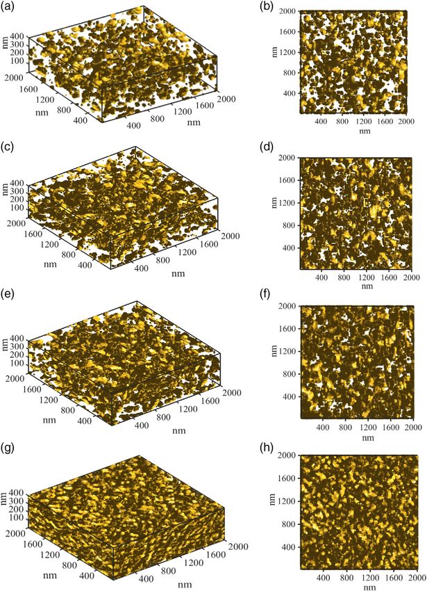
www.advancedsciencenews.com                                                                                           www.advenergysustres.com

configuration has been developed to study the effect of carrier            used MC simulations to study the magnetic properties of a dou-
diffusion length on the performance of PSCs.[11,12]                       ble perovskite nano-Sr2VMoO6.[56] MC simulations have previ-
   It is to be noted that 1D and 2D models based on closed-               ously been used to study domain behaviors from molecular
form solutions of partial differential equations cannot adequately        rotation in hybrid perovskites,[57] realignment of CH3NH3þ
simulate the realistic 3D morphology of PSC device geometry. To           dipoles within 3D CH3NH3PbI3 lattice,[58] 2D van der Waals
address this issue, Monte Carlo (MC) simulation that uses the             growth of 3D parent MAPbCl3,[59] heat capacity and electric polar-
probabilistic and statistical approach is essential.[13] However,         ization of CH3NH3þ cations in CH3NH3PbX3 (where X ¼ I,
MC with the time evolution of processes termed kinetic MC                 Br, Cl),[60] and charge screening by the MAþ dipoles in
(KMC) has the capability to transform a system from one state             MAPbI3.[61] Xue et al. used the 1D MC simulation on a
into another by calculating all transition rates and then randomly        mesoporous-structured PSC to investigate the effects of model-
choosing one transition for execution.[20,21] Fortunately, micro-         ing parameters on PV performance.[62] Sitapure et al. proposed
scopic models based on KMC simulation have been developed                 KMC simulations to study lead halide perovskite quantum dots
to describe charge carrier behavior (e.g., charge carrier genera-         (CsPbBr3 QDs).[63] The inverse relationship between the crystal
tion, dissociation, recombination, and transport) in organic solar        size of CsPbBr3 QDs and [Br]sol has been shown by this model
cells.[22–24]                                                             and validated against experimental data.[63] In 2018, Gagliardi
   The KMC method has helped to generate vital findings in                 and Abate studied the role of the mesoporous TiO2 (m-TiO2)
experimental data by closely simulating charge transfer,[23,25]           interface between the electron transport layer (ETL) and the
carrier mobility, geminate,[24] and bimolecular recombination.[22]        perovskite.[64] They used a 1D model in the planar case and
This method has been considered a useful tool for studying,               the MC-based “metropolis” algorithm to make the 3D morphol-
understanding, and improving the performance of organic solar             ogy of the device in the mesoscopic case. They reported that the
cells[26–33] and silicon solar cells.[34,35]                              mesoscopic structures were highly tolerant of ion vacancy migra-
   The KMC simulation approaches can be applied for charge                tion than the planar structure. However, no attempt has been
transport modeling. There are two kinds of transition rates for           made on modeling and simulating a complete PSC using the
charge carrier transport defined based on Miler Abraham                    KMC approach. A substantial need exists to develop a realistic
(MA), used for disorder structure, and the Marcuse theory, used           model to simulate 3D PSC to probe morphological variations
for polaron structure.[36,37] Methylammonium lead iodide                  and their impacts on device performances.
(MAPbI3) PSCs have the disorder structures[38–40] and energy                 In this work, we demonstrated modeling the 3D morphology
disorder.[41] Energy disorder is accompanied by structure disor-          of the perovskite-based film and solar cells enabled by the KMC
der,[42] and Gaussian distribution was usually utilized to model          method. As the KMC method has demonstrated great potential
the density of states (DOS) in disorder semiconductors.[41,43,44]         in temporal modeling of 3D morphology, charge transport mech-
There are two main charge transport models: multiple trapping             anisms, and charged particle generation/recombination, it is
and hopping in disordered materials.[45,46] The multiple trapping         more representative of the realistic natural phenomena that
model transport occurs through extended states, but the trans-            occur in solar cells. We developed a new KMC model to assist
port process is impeded due to multiple trapping and detrapping           fabrication conditions for PSCs. This model can predict PV
events in the localized states.[45] At this time, it is unclear whether   performance, including open-circuit voltage (Voc), short circuit
the multiple trapping model can effectively be used.[45,47,48] One        current density ( Jsc), fill factor (FF), and efficiency (η). KMC
reason may be that the particular structure of disordered materi-         simulation results showed that the perovskite films with the
als does not allow for extended states. For this kind of materials,       pin holes-free, homogenous perovskite capping layer and an opti-
carrier jumps between localized states through tunneling and/or           mized thickness of 400 nm gave the highest PV efficiency of
thermal activation appear to be the preferred charge transfer             20.85%. We found short apparent charge transport time and
mechanism; this mechanism might be much better understood                 long apparent charge carrier recombination lifetime in the high-
through use of the hopping model.[45] The rate of carrier hopping         est performance device. With the demonstration of validation of
depends on the energy difference between the localized states             simulation against experimental results, this new model can
and the spatial distance between them.[45,46] Ma and Wang                 serve as a reliable tool in the accurate prediction of PSC
reported that the charge density of the conduction band mini-             performance.
mum (CBM) and the valence band maximum (VBM) are local-
ized in nanoscale with the size of a few nanometers because of
the random orientation of the organic molecule CH3NH3 in                  2. Simulation Methodology
CH3NH3PbI3.[49] Doping the TiO2 layer underneath the perov-
skite causes narrowing of the depletion region at the interface,          Morphology of a PSC with an initially randomly distributed
thus improving charge carrier tunneling, which facilitates effi-           perovskite, m-TiO2, and spiro-OMeTAD will be generated using
cient charge transport via the high-resistance TiO2 layer.[50–53]         the Metropolis algorithm and the Ising model[13,27,58,65] with a
We think that Gaussian DOS and that charge transport occurs               size of 2000 nm  2000 nm  900 nm. We consider compact
via hopping are a valid theory to apply for charge transport in           TiO2 (c-TiO2) as an ETL and spiro-OMeTAD as a hole transport
the mesoscopic MAPbI3 solar cell because of a disordered struc-           layer (HTL) with a free charge carrier density of 5  1019 cm3
ture,[1–3] energy disorder,[4] localized states,[49] and charge carrier   and 3  1018 cm3, respectively.[14] The ETL and HTL are parallel
tunneling.[50–53]                                                         to an xy plane located at 0 < z ≤ 50 and 700 < z ≤ 900 with a
   As the PSC is still a new field, the fundamental device mech-           thickness of 50 and 200 nm. The active layer sites were distrib-
anisms are still not well understood.[54,55] In 2013, El Yadari et al.    uted with a density of 2.5  1020 cm3[14] by considering m-TiO2

Adv. Energy Sustainability Res. 2021, 2000068        2000068 (2 of 13)               © 2021 The Authors. Advanced Energy and Sustainability Research
                                                                                                                     published by Wiley-VCH GmbH
www.advancedsciencenews.com                                                                                             www.advenergysustres.com

and perovskite located at 50 < z ≤ 300 with a thickness of 250 nm                KTμch
                                                                         Dch ¼                                                                    (3)
plus capping layer located at 300 < z ≤ 700 with a thickness of                    e
400 nm. The morphological parameters such as capping layer
thickness were altered by changing z-dimension of the device,               Considering an electron mobility of 6  103 cm2 V1 s1
and the perovskite/spiro-OMeTAD ratio was changed by varying             for m-TiO2 and a hole mobility of 50 cm2 V1 s1 and
the number of assigned sites in the volume of the device. After          1  104 cm2 V1 s1 for perovskite and spiro-OMeTAD, respec-
the generation of morphology, neighbor sites (within 3 nm                tively,[14] the corresponding electron and hole diffusion pre-
radius of each site) were tracked that would be used later in            factors were calculated as 0.286 ps1, 2.39 fs1, and 0.0048 ps1.
the moving particle. To enable a continuous transition in the               To consider charge recombination, we used the following
material distribution from one face of the periodic lattice box          equation.
to the next, the periodic boundary conditions were applied in
both x- and y-directions.[64]                                            RCR ¼ wCR expð2γr ij Þ                                                  (4)
   CBM and VBM of c-TiO2, m-TiO2, perovskite, and spiro-
OMeTAD were assigned as 4.1 eV/7.3 eV, 4.1 eV/
7.3 eV,[66,67] 3.93 eV/5.4 eV, and 2.1 eV/5.3 eV,[68–70]            where WCR is a constant recombination rate chosen as 35 μs1 by
respectively. The CB/VB levels with a Gaussian energy distribu-          considering the total charge recombination rate (monomolecu-
tion of 0.1 eV standard deviation were distributed to each site.[14]     lar, bimolecular electron–hole recombination, and Auger recom-
The capping layer is 2000 nm  2000 nm  400 nm in the x-, y-,           bination),[74,75] and other symbols are described as mentioned
and z directions, respectively. The CBM of ETL (4.1 eV) and             earlier.
VBM of HTL (5.3 eV) were selected to collect separated charge              Photon illumination leads to charge generation based on the
carriers in PSCs efficiently. Therefore effective built-in voltage        following equation.
(Vbi) was 1.2 eV. The potential distribution across the active layer
can be modeled as a linear function of the distance within the                   Zλ2 ZL
perovskite layer as supported in a prior report.[9] Applying geo-        Gx ¼              ð1  RðλÞÞ  φs ðλÞ  expðαðλÞxÞ  αðλÞ dλdx          (5)
metric analysis to the potential distribution (Figure S11,                        λ1   0
Supporting Information), it is shown as V bi V  L
                                                   A
                                                      ¼ ψðzÞ
                                                        Lz , where
VA is the applied bias, and z and L are the distance from the start-     where R(λ) and ϕs(λ) are the reflectance of solar cell surface and
ing point of the active layer and the thickness of the active layer,     photon flux density at the surface, respectively. λ1 and λ2 are the
respectively. Consequently, the potential distribution energy ψ(z)       absorption wavelength range of the active material, and L is the
with respect to the z-axis can be stated as                              thickness of the active layer. α(λ) is the absorption coefficient at
                            V bi  V A                                   that wavelength, and x is the depth.[76] Photon illumination
ΨðzÞ ¼ ðV bi  V A Þ                  z                           (1)   under 1.5 AM sunlight gives the generation rate (Gx ) of
                                 L
                                                                         2.5nm3 s1 .[8] GðsÞ ¼ s  Gx ð100Þ used to consider the effect
   Charge transport within the crystallite site, charge recombina-       of perovskite surface coverage (s) on generation rate, where
tion, and extraction by the electrodes are three events that affect      Gx ð100Þ is the generation rate in the active layer for a device with
charge carrier collection. Charge transport in the disordered semi-      100% surface coverage.[77]
conductor is governed by Miller Abraham’s theory,[37] so this the-          To consider coulombic interaction in the model, we used the
ory is a valid theory to apply for charge transport in the MAPbI3        following equation
material because of having a disordered structure[38–40] and energy
disorder.[41] We calculated the charge transport rate (Rch) of elec-              q1 q2
                                                                         En ¼                                                                     (6)
trons in CB sites and holes in VB sites of both TiO2 and perovskite             4πε0 εr r 1,2
layers and used them to simulate illuminated current density–
voltage ( J–V) under applied bias conditions.[29]                        where En is the coulombic energy at site n resulting from charges
                           (                                           q1 and q2 at sites 1 and 2 having distance r1,2. εr and ε0 are the
                                     E E
                             exp  jkT i ∶E j > E i                      relative and absolute permittivity, which equals 24.1 and
Rch ¼ w0ch expð2γr ij Þ
                                   1        ∶E j ≤ E i           (2)     8.85  1014 F cm1, respectively.[72] The distance up to which
         6KTμch                                                          a charge can experience the coulombic force of attraction from
 w0ch ¼          expð2γlÞ                                                another charge is the coulombic cutoff radius. It was calculated
            el2
                                                                         as 3 nm by equating thermal (kBT~25 meV) and coulombic
   In the abovementioned equations, w0ch is the charge hopping           energy inside the device.
pre-factor, and γ is the inverse localization radius taken as               The transport layers are kept neutral during the course of the
2 nm1, because average localization size is considered as               simulation. This was carried out by adding/removing a free car-
0.5 nm.[49]E i and E j indicate the energy of the site for given         rier generated within 3 nm from the contacts to/from the trans-
charge particles at two sites of i and j. r ij is the distance between   port layers if a free carrier is injected to/extracted from the active
two sites of interest. The l is the average charge transfer distance     layer. Equation (7) was used to calculate the injection (dark cur-
taken as 0.64 nm.[71] The diffusion coefficient (Dch) can be              rent) and extraction (photocurrent) carriers in our simulation by
extracted from the Einstein equation using charge carrier mobil-         considering the free carrier density of 5  1019 cm3 in the ETL
ity for electrons and holes (μch ).[72,73]                               and 3  1018 cm3 in the HTL.[14]

Adv. Energy Sustainability Res. 2021, 2000068       2000068 (3 of 13)                  © 2021 The Authors. Advanced Energy and Sustainability Research
                                                                                                                      published by Wiley-VCH GmbH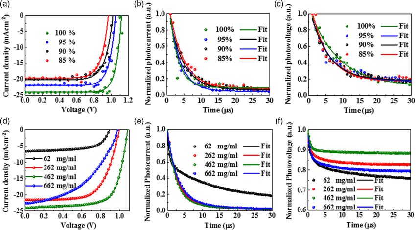
www.advancedsciencenews.com                                                                                                   www.advenergysustres.com

Δninjection ¼ n0ETL  neETL             if n0ETL > neETL                    ∇:J H
                                                                                    h ¼ 0, ∇:J e ¼ 0
                                                                                               E

Δnextraction ¼ nex  n0ex               if nex > n0ex                       ∇:J Ph ¼ GP  RP
                                                                        (7)
Δpinjection ¼ n0HTL  nhHTL             if n0HTL > nhHTL                    ∇:J Pe ¼ GP  RP                                                        (9)

Δpextraction ¼ nhx  n0hx               if nhx > n0hx                       ∇:J M
                                                                                    h   ¼   GM      RM
                                                                                ∇:J M
                                                                                    e   ¼   GM    RM
where n0ETL and n0HTL are the number of electrons and holes                   where G and R are the charge generation and recombination rate,
in 50 nm of ETL and 200 nm of HTL on the thermal equilibrium                    respectively. Jh and Je are the current density induced by holes
condition, respectively. n0ex and n0hx are the number of elec-                and electrons, respectively. H, E, P, and M (in the subscript) indi-
trons and holes within a 3 nm strip of ETL and HTL on the ther-                 cate hole transport, electron transport, perovskite capping, and
mal equilibrium condition, respectively. neETL and nex are                    m-TiO2 layer, respectively.
electron concentration in 50 nm and within a 3 nm strip of
ETL, respectively. nhHTL and nhx are hole concentration in
200 nm and within a 3 nm strip of HTL, respectively. The total                  3. Results and Discussion
number of free carriers (nc) is calculated in the transport layers by
the following equation in the time step (Δt).[78]                               Figure 1a shows the mesoscopic structure of an n-i-p PSC.
                                                                                Appropriate electronic band alignment among ETL, HTL, and
        1 X n
               δti                                                              perovskite absorber layer is required for optimal device perfor-
nc ¼                                                                    (8)     mance. Electrons need to transfer from perovskite to ETL,
       AΔz i¼1 Δt
                                                                                whereas holes need to transfer from perovskite to HTL without
                                                                                any significant energy loss. The KMC simulation can visualize
   AΔz , δti are the volume of the transport layer and the time                 the energy band diagram of PSCs. Figure 1b,c shows the ener-
spent by the charge i in the transport layer, respectively. To be               getic disorder for full coverage of capping layer with perovskite
comparable with the relaxation time of the transport layers,                    related to localized sites with a slice of (29 ≤ x ≤ 30 nm,
the time step of 1 ps is chosen.[79] Then, the net charge                       20 ≤ y ≤ 30 nm) with a band bending of CBM and VBM levels
extracted/injected is calculated and plotted against time (Q–t)                 at 0 V and 1.10 V, respectively. Due to the weak electric field
under any given voltage condition. To reach the electric current,               in the absorber layer by applying a forward bias of 1.10 V, the
we used the least squares method to fit a line to the Q–t plot and               band bending changes to a flat band. The CBM and VBM offsets
read the slope of the line.                                                     decrease, as the band bending changes to a flat band by applying
   The governing equations to simulate the illuminated J–V                      forward bias. Figure S1, Supporting Information, shows the
are[62]                                                                         energy band diagram of partial coverage of the capping layer.

Figure 1. a) Structure of an n-i-p PSC, visualization of the energy band diagram of full coverage capping layer PSC by KMC simulation b) under thermal
equilibrium and c) under 1.10 V forward bias.

Adv. Energy Sustainability Res. 2021, 2000068               2000068 (4 of 13)                © 2021 The Authors. Advanced Energy and Sustainability Research
                                                                                                                             published by Wiley-VCH GmbH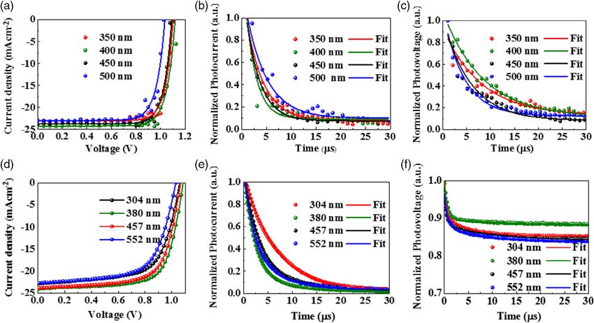
www.advancedsciencenews.com                                                                                            www.advenergysustres.com

Figure 2. Simulated morphology of PSCs with different coverage of capping layer volume 3D image and top view: a,b) 85%, c,d) 90%, e,f ) 95%, and
g,h) 100%.

   We developed a model to simulate the perovskite morphology             interface properties and PV performance, the pin holes-free,
using a Metropolis algorithm. Figure 2 shows the 3D (Figure 2a,           homogenous perovskite capping layers are critical.[80–82] In our
c,e,g) and top view (Figure 2b,d,f,h) simulated morphology of the         simulation, the charge generation increased with increasing cov-
perovskite capping layer, respectively, each demonstrating 85%,           erage of the capping layer. The incomplete coverage led to poor
90%, 95%, and 100% coverage of film volume. The yellowish-                 charge transport pathways for the electron and hole diffusion.
brown regions in the simulated morphology are assigned to                 Also, the gap fraction was filled with spiro-OMeTAD, which
perovskite, whereas the white regions are assigned to the gap             has charge transport rate 106 times less than the perovskite.
and pinholes between perovskite grains.                                   This increased recombination events. Therefore, the perfor-
   Figure 3a displays the simulated J–V characteristics of PSC            mance of PSC decreased by decreasing the perovskite coverage
with different coverage of capping layer volume. The capping              in the capping layer. Voc was found to increase with higher
layer thickness used for simulation was 400 nm. Table 1 lists             coverage of the capping layer (Table 1). Previous reports[77]
the simulated device performance of PSCs, charge carrier trans-           showed that Voc is dependent on surface coverage (s)
port time (τt), and charge carrier recombination lifetime (τr) for                                      h          i              J
                                                                                                          ð1sÞβþs
different coverage of capping layer volume. To reach effective            as V OC ðsÞ ¼ V OCEPH  mkT
                                                                                                   q  ln      s      , where β ¼ J 0EH . The
                                                                                                                                         0EPH

Adv. Energy Sustainability Res. 2021, 2000068       2000068 (5 of 13)                 © 2021 The Authors. Advanced Energy and Sustainability Research
                                                                                                                     published by Wiley-VCH GmbH
www.advancedsciencenews.com www.advenergysustres.com
Figure 3. a–c) Simulated and d–f ) experimental ( J–V curves, TPC decay, and TPV decay with different coverage of capping layer volume), showing 100%
coverage and 462 mg mL1 concentration of PbI2 (100% coverage) with the best PV performance, shortest apparent charge transport time, and longest
apparent carrier recombination lifetime for simulated and experimental, respectively.
Table 1. Simulated device performance, charge carrier transport, and The values of τt and τr (Table 1) are in good agreement with the
lifetime for different coverage of capping layer volume (85%, 90%, J–V characteristics results. The lower values of τt and higher val-
95%, and 100%) of the fabricated PSCs. ues of τr suggest a higher probability of charge separation, extrac-
tion, and collection, which is supported by higher values of
Coverage of capping Jsc [mA cm2] Voc [V] FF Efficiency τt [μs] τr [μs]
Voc and FF and eventually higher efficiency. The τr is longer than
layer volume [%] [%]
τt for all different coverage of the capping layer. As the coverage
85 19.83 0.97 0.72 13.84 4.16 5.95 of the capping layer increased, τt decreased, whereas the τr
90 20.2 1.02 0.73 15.04 4.11 6.15 increased. At 100% cell coverage, we observed the lowest τt,
95 21.94 1.05 0.76 17.5 3.21 6.56 and the highest τr.
100 24.09 1.11 0.78 20.85 2.14 8.32 To relate these simulation results with experimental results,
various PSCs with different coverage of perovskite capping layer
were fabricated. We accomplished this by varying the PbI2 con-
centration for perovskite film formation. X-ray diffraction (XRD)
subscript EPH indicates perovskite between ETL and HTL, patterns were recorded to understand the effect of different PbI2
whereas EH means the absence of perovskite. J0 and m are concentrations on perovskite crystallinity. Figure S2, Supporting
the dark saturation current density and diode ideality factor, Information, shows the XRD patterns of perovskite films pre-
respectively. k, T, and q are Boltzmann’s constant, absolute tem- pared by different PbI2 concentrations (62, 262, 462, and
perature, and elementary charge constant, respectively. 662 mg mL1). The observed peaks at 14.08 , 28.41 , 31.85 ,
Figure 3b,c shows the transient photocurrent (TPC) and pho- and 43.19 are assigned to (110), (220), (310), and (330) crystal-
tovoltage (TPV) decays. We calculated TPC using an equation line planes of CH3NH3PbI3 confirming its tetragonal crystal
IðtÞ ¼ ΔqðtÞ
Δt by considering the total collected charges. TPV was structure.[83,84] The incomplete conversion of PbI2 to perovskite
obtained using high resistance (14 kΩ cm2) at near open-circuit leads to the peak (001) at 12.12 that corresponds to PbI2.[2,84,85]
voltage. We obtained apparent charge transport time and carrier XRD results show that the crystallinity of perovskite increased by
recombination lifetime by fitting the decay function with mono- increasing PbI2 concentration. The 662 mg mL1 samples com-
exponential equation Aet=τ , where τ is the apparent charge trans- pared with the other perovskite samples have a large peak at
port time (τt) in TPC and apparent carrier recombination lifetime 12.12 . It indicates the existence of more PbI2 in this perovskite.
(τr) in TPV.[83] The τt of 2.14 μs and the τr of 8.32 μs were found The PbI2 layer becomes more compact when the PbI2 concentra-
for the highest efficiency device at the 100% coverage of capping tion is higher than 462 mg mL1. It may be lead to an incomplete
layer volume. The τr is longer than the τt, ensuring that generated reaction of PbI2 with CH3NH3I.[86] The fabrication approach was
carriers reach the electrode before recombination. included in the Supporting Information.
Adv. Energy Sustainability Res. 2021, 2000068 2000068 (6 of 13) © 2021 The Authors. Advanced Energy and Sustainability Research
published by Wiley-VCH GmbHwww.advancedsciencenews.com www.advenergysustres.com
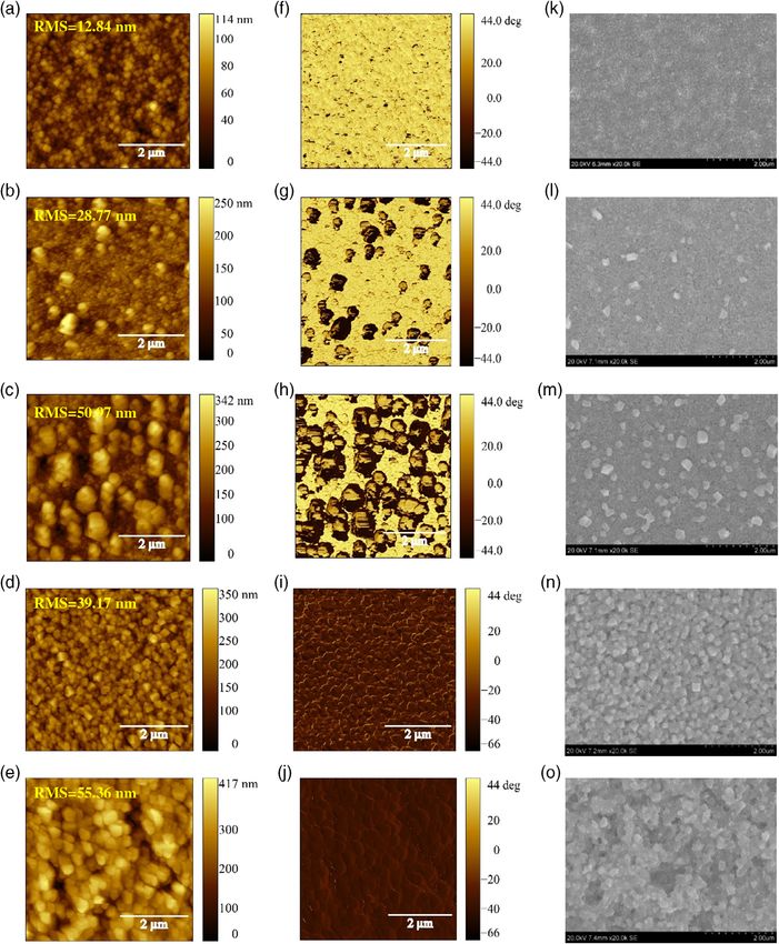
Figure 4. a–e) AFM topography, f–j) phase images, and k–o) SEM images: a,f,k) FTO/compact TiO2/m-TiO2; perovskite films on top of m-TiO2 with
different concentrations of PbI2: b,g,l) 62 mg mL1, c,h,m) 262 mg mL1, d,i,n) 462 mg mL1, and e,j,o) 662 mg mL1, showing 462 mg mL1 of PbI2 is
the optimized concentration to achieve most homogenous and pin holes-free perovskite.
Figure 4 shows the atomic force microscope (AFM) topography gaps increased again and led to a non-homogenous perovskite
(Figure 4a–e), AFM phase (Figure 4f–j), and the scanning electron capping layer.
microscope (SEM) (Figure 4k–o) images of fluorine-doped tin The comparison between phase image of m-TiO2 (Figure 4f )
oxide (FTO)/compact TiO2/m-TiO2/perovskite films with different with phase images of perovskite film with lesser PbI2 concentra-
concentrations of PbI2. These images show the decreasing tion (62 and 262 mg mL1) (Figure 4 g,h) shows partial coverage
gap between perovskite crystals by increasing PbI2 concentration of perovskite crystals. A similar observation can be made with a
until the optimized concentration (462 mg mL1) with a homoge- comparison between SEM images (Figure 4k–m). On the other
nous perovskite capping layer. At high PbI2 concentration, the hand, perovskite film at optimized and higher than optimized
Adv. Energy Sustainability Res. 2021, 2000068 2000068 (7 of 13) © 2021 The Authors. Advanced Energy and Sustainability Research
published by Wiley-VCH GmbHwww.advancedsciencenews.com www.advenergysustres.com
Table 2. PV parameters, apparent charge transport time, and carrier recombination lifetime for PSCs prepared with the different concentrations of PbI2
(62, 262, 462, and 662 mg mL1).
Concn of PbI2 Jsc [mA cm2] Voc [V] FF Efficiency [%] τt [μs] τr [μs]
[mg mL1]
Forward Reverse Forward Reverse Forward Reverse Forward Reverse
62 6.65 6.59 0.89 0.9 0.6 0.62 3.55 3.68 7.49 5.02
262 21.58 21.59 0.98 1 0.6 0.65 12.61 13.93 4.85 5.69
462 24.04 24.06 1.01 1.09 0.63 0.7 15.3 18.36 2.44 7.24
662 22.47 22.55 0.93 0.98 0.37 0.46 7.73 10.19 4.34 5.09
PbI2 concentration shows the full coverage, but the high crystallin- respectively, indicating efficient charge extraction with a high-
ity of perovskite at 662 mg mL1 caused to non-homogenous quality perovskite layer formation with reduced gaps. This is sup-
perovskite. The higher perovskite film roughness in 662 mg mL1 ported by the observed increased Jsc and Voc for cells with
may hinder charge transport in the film and across the perovskite/ 462 mg mL1 PbI2 concentration. Meanwhile, the cell with
charge transport layer interface. It was also reported that the 62 mg mL1 showed the longest τt of 7.49 μs and the shortest
unreacted PbI2 may act as a barrier for electron injection at the τr of 5.02 μs caused by more gaps and pinholes. Our measured
TiO2/perovskite interface.[86] apparent τt and τr values are in good agreement with other
Figure 3 d–f shows the reverse scan of J–V characteristics, reports on the perovskite films.[88–91]
TPC, and TPV decay of CH3NH3PbI3 solar cells fabricated Simulation and experimental results include the efficiencies,
with the different PbI2 concentrations (62, 262, 462, and τt and τr, of solar cells simulated with different capping layer
662 mg mL1), respectively. As shown in Table 2, after increas- coverage and solar cells fabricated with different PbI2 concentra-
ing the PbI2 concentration from 62 to 462 mg mL1, the average tions, respectively. The efficiencies, τt and τr, of PSCs improved
efficiency was found to increase from 3.55% in the forward scan by increasing the coverage of the capping layer (as shown in
and 3.68% in the reverse scan for 62 mg mL1 device to 15.30% Table S1, Supporting Information). PSCs with homogenous
in the forward scan and 18.36% in the reverse scan for and pinhole-free perovskite capping layer (100% coverage)
462 mg mL1 device. achieved maximum efficiency in simulation, and experimental
The further increase in PbI2 concentration to 662 mg mL1 results showed optimal efficiency at 462 mg mL1 PbI2 concen-
led to a decrease in efficiency. The higher concentration of tration. Also, τt and τr are, respectively, the shortest and longest
PbI2 led to higher absorption of photons, as shown in Figure S3a, in 100% coverage of the capping layer and 462 mg mL1 PbI2
Supporting Information. However, a high amount of PbI2 con- concentration for simulated and experimental PSC. Perovskite
centration will cause reduced charge transport because of an film at optimized (462 mg mL1) and higher than optimized
increase in the surface roughness (Figure 4e) and thickness of (662 mg mL1) PbI2 concentration show full coverage, but the
the capping layer[87] that results in charge recombination before high crystallinity of perovskite at 662 mg mL1 resulted in
reaching charge extraction layers. Homogenous and pin holes- non-homogenous and rougher perovskite film morphology (as
free perovskite capping layer is critical to reaching good interface shown in Figure 4e). The higher perovskite film roughness in
properties and PV performance,[80–82] and 462 mg mL1 of PbI2 662 mg mL1 is likely to impede charge transport in the film
is the optimized concentration to achieve this. The integrated Jsc and across the perovskite/charge transport layer interface. It is
from the incident photon-to-current efficiency (IPCE) spectra in also reported that for higher concentrations of PbI2, the
Figure S3b, Supporting Information, is in good agreement with unreacted PbI2 may act as a barrier for electron injection at
Jsc calculated from J–V characterization. the TiO2/perovskite interface.[86] Therefore, the performance
We carried out TPC and TPV measurements for further of the perovskite cell decreased for 662 mg mL1 of PbI2 concen-
insights into charge transport. Figure 3e, f shows the TPC tration and did not follow the trend as presented in Table S1,
and TPV decay curves of PSCs prepared with the different con- Supporting Information.
centrations of PbI2 (62, 262, 462, and 662 mg mL1). The short- The thickness of the capping layer was varied by changing the
lived photocurrent is generated by a nanosecond pulse of a dye z-dimension of the device. Figure S4, Supporting Information,
laser incident on solar cells under short circuit conditions (by a displays the device morphologies with different capping layer
very low resistor at 50 Ω) and open circuit conditions (by a very thicknesses by considering full coverage of the perovskite cap-
high resistor at 1 MΩ) to approximate open circuit. ping layer. The z-dimensions were varied in the step of 50 nm
The TPV decay does not reach zero level in Figure 3f, because, to give a capping layer thickness of 350 nm, 400 nm, 450 nm,
in the TPV measurement, the background light intensity of and 500 nm. Capping layer thickness was obtained after deduct-
1.5 sun was used to illuminate the cells. Apparent charge trans- ing 50 nm for compact TiO2 (c-TiO2) (ETL), 250 nm for m-TiO2,
port time and carrier recombination lifetime were obtained by and 200 nm for spiro-OMeTAD (HTL) from z-dimension of the
mono-exponential fitting as done earlier. Table 2 summarizes device.
the observed values of τt and τr for PSCs prepared with a different Figure 5a shows the simulated J–V curves under the illumi-
concentrations of PbI2. The τt and τr of perovskite films prepared nation condition by considering the different thicknesses of
by 462 mg mL1 are shortest (2.44 μs) and longest (7.24 μs), the capping layer. The simulated J–V curves show that the
Adv. Energy Sustainability Res. 2021, 2000068 2000068 (8 of 13) © 2021 The Authors. Advanced Energy and Sustainability Research
published by Wiley-VCH GmbHwww.advancedsciencenews.com www.advenergysustres.com
Figure 5. a–c) Simulated and d–f ) experimental ( J–V curves, TPC decay, and TPV decay with different thicknesses of the capping layer), showing the
capping layer with a thickness of 400 nm and 380 nm with the best PV performance, shortest apparent charge transport time, and longest apparent carrier
recombination lifetime for simulated and experimental, respectively.
Table 3. Simulated device performance of PSCs, charge carrier transport, Figure 5b,c shows the TPC and TPV decay by considering the
and lifetime with a varying thickness of the capping layer. different thicknesses of the capping layer. The transient decays
were calculated using the same approach described earlier in dif-
Capping layer Jsc [mA cm2] Voc [V] FF Efficiency [%] τt [μs] τr[μs] ferent coverage of the capping layer. The values of τt and τr
thickness [nm] (Table 3) are in good agreement with the J–V characteristics
350 23.17 1.09 0.77 19.44 3.47 7.98 results. At lower thickness, the low absorption causes insufficient
400 24.09 1.11 0.78 20.85 2.14 8.32
charge carrier collection. Therefore, the charge carrier will accom-
modate certain sites with a longer distance between each charge
450 23.84 1.07 0.76 19.38 2.83 5.83
carries. The coulombic interaction will decrease as a result of the
500 23.07 1.03 0.74 17.58 3.77 4.55
long distance between each carrier. Therefore, the apparent charge
transport time is longer, and the carrier recombination lifetime is
shorter. On the other hand, at the larger thickness, more light
thickness of the perovskite layer has a critical role in device effi- absorption, and, hence, more charge carriers, therefore, the prob-
ciency. Table 3 shows the simulated device performance of PSCs, ability of recombination will increase. This explains the increase in
τt, and τr with varying thickness of the capping layer. The capping apparent charge transport time and the decrease in carrier recom-
layer thickness of PSCs has a direct relation with photon absorp- bination lifetime. At an optimized thickness of 400 nm, position-
tion. The higher thickness of the capping layer leads to higher dependent coulombic interaction between charge carriers is
absorption of photons.[81,92] However, a larger thickness of the optimized where a balance exists between the carrier collection
capping layer will cause reduced charge transport. The device efficiency and the photogenerated charge carrier.
efficiency was low in the capping layer with 350 nm thickness PSCs were fabricated with varying capping layer thickness to
(Figure S4a, Supporting Information) because of insufficient relate these simulation results with experiments. A sequential
photon absorption. However, the capping layer with a thickness deposition method was used to prepare the perovskite films.
of 500 nm (Figure S4d, Supporting Information) had sufficient Different spin speeds were used to reach various thicknesses.
light absorption but impeded the efficient charge transport to Figure 5d–f shows, respectively, the reverse scan of J–V charac-
electrodes. This was due to the longer pathway that triggers teristics, TPC, and TPV of CH3NH3PbI3 PSCs fabricated with the
higher chance of charge recombination before reaching charge PbI2 films spin-coated at different spin speeds from 2000 to
extraction layers (TiO2 and spiro-OMeTAD). Consequently, we 5000 rpm at a step of 1000 rpm. This led to various capping layer
found efficiency to be lower in the device with a thicker capping thicknesses from 304 to 552 nm. The thicker layers were fabri-
layer. The highest efficiency of 20.85% in the simulation was cated at slower spin speeds. Veeco Dektak 150 profilometer was
obtained with an optimized perovskite capping layer thickness used to measure the prepared film thickness. The fabrication
of 400 nm. approach was included in the Supporting Information.
Adv. Energy Sustainability Res. 2021, 2000068 2000068 (9 of 13) © 2021 The Authors. Advanced Energy and Sustainability Research
published by Wiley-VCH GmbHwww.advancedsciencenews.com www.advenergysustres.com
Table 4. PV parameters, apparent charge transport time, and carrier recombination lifetime for PSCs with different capping layer thicknesses (304, 380,
457, and 552 nm).
Capping layer Jsc [mA cm2] Voc [V] FF Efficiency [%] τt [μs] τr [μs]
thickness [nm]
Forward Reverse Forward Reverse Forward Reverse Forward Reverse
304 22.71 22.86 1.03 1.06 0.65 0.65 15.2 15.75 6.31 6.83
380 24.04 24.06 1.01 1.09 0.63 0.7 15.3 18.36 2.44 7.24
457 23.1 23.86 1.02 1.07 0.6 0.68 14.14 17.36 3.68 5.03
552 22.8 22.71 0.96 1.03 0.6 0.65 13.13 15.2 3.79 4.79
As shown in Table 4, the average efficiency was found to has reported a wide range of εr values from 22 to 30.[72,96–99] This
increase with an increase in the capping layer thickness from is why we chose the εr values at 22,[96] 24.1,[72] and 30[99] to cover
304 to 380 nm and decrease with further increasing the thickness this reported range. Figure S10, Supporting Information, shows
to 457 and 552 nm. The cell with 380 nm thick perovskite cap- the simulation results of device efficiency, apparent charge trans-
ping layer achieved the highest efficiency of 18.36% versus port time, and charge carrier lifetime as a function of capping
15.75% for the cell with the 304 nm thick capping layer. layer thickness by considering these three different values of
The improvement is reflected in all the other PV parameters, dielectric permittivity. The optimal thickness of the capping layer
too. This improvement can be attributed to the improved charge is all at 400 nm for the three different dielectric permittivities at
transport properties and reduced recombination.[93,94] 22, 24.1, and 30. At this optimal thickness, the PSCs exhibited the
Figure S5a, Supporting Information, shows the absorption of highest PV efficiency, shortest apparent charge transport time,
photons increased by increasing the capping layer thickness. and longest apparent charge carrier lifetime for all three different
However, cells with a thickness exceeding the optimized thick- dielectric permittivities. However, a higher εr value leads to
ness (380 nm) will suffer reduced charge transport; a longer higher PV performance. With increasing value of dielectric per-
charge carrier pathway leads to charge recombination before mittivity, the PV performance improved because of decreasing
reaching the charge extraction layers.[94,95] The IPCE spectra charge recombination and coulombic interaction.[100–102]
shown in Figure S5b, Supporting Information, also support
the results with Jsc values in good agreement with that obtained
from the J–V measurements. 4. Conclusion
Figure 5e,f shows the TPC and TPV of PSCs prepared with a
different thickness of the capping layer (304, 380, 457, and We achieved the demonstration on the modeling of the 3D mor-
552 nm). As shown in Table 4, the τt and τr of perovskite films phology of perovskite-based film and solar cells enabled by the
with the 380 nm thick capping layer are shortest and longest, KMC method. A highly accurate simulator to model PSCs was
respectively, showing efficient charge extraction and highest created to predict PV performance via KMC simulation. As
open-circuit voltage. These results agree with IPCE and J–V char- the KMC method is based on possible transition rates, this work
acteristics where enhanced Jsc, Voc, and highest device efficiency produced a high accuracy 3D model by considering physical pro-
were achieved for the cell with the 380 nm thick capping layer. cesses (e.g., charge generation, charge transport, and charge
However, τt is the longest (6.31 μs) for the cell with 304 nm thick- recombination) in PSCs. KMC simulation shows that the highest
ness, which may be caused by less absorption. However, the device performance comes from using the full coverage capping
perovskite cell with the thickest capping layer (552 nm) has layer perovskite films with a thickness of 400 nm. The highest
the shortest τr (4.79 μs) owing to more recombination. Our mea- performance device exhibited short apparent charge transport
sured apparent τt and τr values are in good agreement with other time and long apparent charge carrier recombination lifetime.
reports on the perovskite films.[88–91] This work demonstrates that the KMC method is a powerful
Figure S6, Supporting Information, shows the comparison of approach to model PSCs. With the demonstration of validation of
efficiencies, apparent charge transport time, and carrier recom- simulation against experimental results, this new model can
bination lifetime from simulation and experimental results. serve as a reliable tool in the realistic prediction of PSC perfor-
PSCs with a capping layer thickness of 400 nm gave optimum mance. This model may provide a significant conceptual advance
efficiency in simulation, and experimental results showed opti- in identifying bottlenecks and guiding novel device designs to
mum efficiency at a spin speed of 4000 rpm, which is equivalent improve PSC performance.
to an active layer thickness of 380 nm. Also, as shown in
Figure S6b,c, Supporting Information, τt and τr are the shortest
and longest in an optimized capping layer thickness of 400 nm 5. Experimental Section
and 380 nm for simulated and experimental PSC, respectively.
Device Fabrication: FTO-coated substrates (1.5 cm 1.5 cm) was used
The εr values of MAPbI3 perovskite systems were reported to
for fabricating PSCs. Zinc powder used for etching FTO substrates and
depend on multiple factors such as experimental methods to pre- then diluted in hydrochloric acid (0.1 mL HCl in 1 mL DI water by volume).
pare the samples and measure εr, and computational methodol- Substrates were subsequently cleaned via sonication with detergent water,
ogies to determine the εr values.[96] Based on this, the literature deionized water, acetone, and isopropanol for 25 min, respectively.
Adv. Energy Sustainability Res. 2021, 2000068 2000068 (10 of 13) © 2021 The Authors. Advanced Energy and Sustainability Research
published by Wiley-VCH GmbHwww.advancedsciencenews.com www.advenergysustres.com
Nitrogen flows to dry substrates, followed by plasma treatment for 20 min conclusions, or recommendations expressed in this article were those of
in the presence of oxygen. the authors alone and do not necessarily reflect the views of USAID or
Compact layers of TiO2 (titanium diisopropoxide bis(acetylacetonate), NAS. The authors would like to thank Dr. Brian Moore for assisting
75 wt% solutions in 2-propanol) prepared from its precursor solutions of them with high-performance computing facility at South Dakota State
0.15 M were spin-coated onto cleaned substrates at 4500 rpm for 45 s and University.
then annealed at 200 C for 10 min. A mesoporous TiO2 (commercial TiO2
paste (30 NRD, Dyesol) diluted in ethanol at a weight ratio of 1:6) was
spin-coated at 5000 rpm for 30 s after the substrates cooling down to room
temperate. After annealing substrates at 450 C for 30 min, it was then
Conflict of Interest
cooled down to room temperature. Substrates were then treated by dip- The authors declare no conflict of interest.
ping them in TiCl4 (25 mM) solution for 30 min at 70 C, followed by rins-
ing with DI water, ethanol, and then annealed at 450 C for 30 min.
PbI2 solution (62, 262, 462, and 662 mg mL1 in dimethylformamide)
was prepared by overnight stirring at 70 C for considering different cov-
Data Availability Statement
erage of the capping layer. The solution was spin-coated on top of a mes- Research data are not shared.
oporous TiO2 layer at 4000 rpm for 40 s; then, they annealed at 70 C for
30 min. The PbI2 films were dipped in CH3NH3I solution (10 mg mL1 in
isopropyl alcohol) to form perovskite layer, followed by immediately spin
coating at 6000 rpm for 10 s. Perovskite films were then annealed at 100 C Keywords
for 15 min.
Spiro-OMeTAD was used as an HTL. Solution prepared by capping layer coverage, capping layer thickness, full perovskite solar cell
mixing 72.3 mg of (2,2 0 ,7,7 0 -tetrakis(N,N-di-p-methoxyphenylamine)-9,9- operation, kinetic Monte Carlo simulation, perovskite solar cells
spirobifluorene) (spiro-OMeTAD), 28.8 μL of 4-tert-butylpyridine,
17.5 μL of a stock solution, and 520 mg mL1 of lithium bis (trifluorome- Received: November 5, 2020
thylsulfonyl)imide in acetonitrile in 1 mL of chlorobenzene. Spiro- Revised: December 25, 2020
OMeTAD was spin-coated on top of perovskite layer at 2000 rpm for Published online:
40 s. Finally, silver (Ag) was then deposited as a top electrode in a high
vacuum chamber using thermal evaporation.
To reach different capping layer thicknesses, 462 mg mL1 of PbI2 solu- [1] G. Saianand, P. Sonar, G. J. Wilson, A.-I. Gopalan, V. A. Roy,
tion was spin-coated on top of a mesoporous TiO2 layer from 2000 to G. E. Unni, K. M. Reza, B. Bahrami, K. Venkatramanan, Q. Qiao,
5000 rpm at the step of 1000 rpm for 40 s. J. Energy Chem. 2020, 54, 151.
Characterization: Absorbance spectra of perovskite films were mea-
[2] A. Dymshits, A. Henning, G. Segev, Y. Rosenwaks, L. Etgar, Sci. Rep.
sured with Agilent 8453 UV-VIS spectrophotometer G1103A. Rigaku
2015, 5, 8704.
Smartlab system was used to recorded XRD spectra. Agilent SPM 5500
AFM equipped with MAC III controller (three lock-in amplifiers) was used [3] H. Elbohy, B. Bahrami, S. Mabrouk, K. M. Reza, A. Gurung,
to map topography and phase with multi75Eg budget sensor tip. The tip’s R. Pathak, M. Liang, Q. Qiao, K. Zhu, Adv. Funct. Mater. 2018,
first resonance ( f1) frequency of 71 kHz was fed into the first lock-in 1806740.
amplifier (LIA1). The vertical tip-sample separation was controlled from [4] K.-F. Lin, S. H. Chang, K.-H. Wang, H.-M. Cheng, K. Y. Chiu,
LIA1, which provided the error in the amplitude signal at first resonance K.-M. Lee, S.-H. Chen, C.-G. Wu, Sol. Energy Mater. Sol. Cells 2015,
( f1) to the servo. This first lock-in amplifier was used for topographic 141, 309.
and phase imaging. The fabricated PSCs were characterized by J–V char- [5] S. Mabrouk, A. Dubey, W. Zhang, N. Adhikari, B. Bahrami,
acteristics. The J–V was measured using Agilent 4155C under the illumi- M. N. Hasan, S. Yang, Q. Qiao, J. Phys. Chem. C 2016, 120, 24577.
nation of a solar simulator (Xenon lamp, Newport) with an intensity of [6] K. M. Reza, A. Gurung, B. Bahrami, S. Mabrouk, H. Elbohy, R. Pathak,
100 mW cm2 (AM 1.5). A National Renewable Energy Laboratory K. Chen, A. H. Chowdhury, M. T. Rahman, S. Letourneau, J. Energy
(NREL) photodetector (S1133 14-01) was used to calibrate the intensity Chem. 2019, 44, 41.
of illumination by setting the distance between the solar simulator and
[7] J. Gong, S. B. Darling, F. You, Energy Environ. Sci. 2015, 8, 1953.
the solar cell. All solar cells with an area of 0.16 cm2 were characterized
[8] J. M. Foster, H. J. Snaith, T. Leijtens, G. Richardson, SIAM J. Appl.
in the same conditions with a 0.5 V s1 scan rate in forward with 0 to 1.1 V
and a reverse scan sweeping from 1.1 to 0 V. The IPCE was measured Math. 2014, 74, 1935.
using a xenon lamp (Newport) attached to a monochromator (Newport). [9] X. Sun, R. Asadpour, W. Nie, A. D. Mohite, M. A. Alam, IEEE J.
The monochromatic light was focused on the active area of the solar cell by Photovol. 2015, 5, 1389.
focusing on two lenses. NREL calibrated photodiodes were used as a ref- [10] Y. Zhou, A. Gray-Weale, Phys. Chem. Chem. Phys. 2016, 18, 4476.
erence for IPCE measurements. [11] K. Fu, Q. Zhou, Y. Chen, J. Lu, S.-E. Yang, J. Optics 2015, 17, 105904.
[12] Q. Zhou, D. Jiao, K. Fu, X. Wu, Y. Chen, J. Lu, S.-e. Yang, Sol. Energy
2016. 123: 51.
Supporting Information [13] A. Gagliardi, A. Abate, ACS Energy Lett. 2017, 3, 163.
[14] F. Liu, J. Zhu, J. Wei, Y. Li, M. Lv, S. Yang, B. Zhang, J. Yao, S. Dai,
Supporting Information is available from the Wiley Online Library or from Appl. Phys. Lett. 2014, 104, 253508.
the author. [15] T. Minemoto, M. Murata, J. Appl. Phys. 2014, 116, 054505.
[16] Y. Wang, Z. Xia, J. Liang, X. Wang, Y. Liu, C. Liu, S. Zhang, H. Zhou,
Semicond. Sci. Technol. 2015, 30, 054004.
Acknowledgements [17] H. Xue, K. Fu, L. H. Wong, E. Birgersson, R. Stangl, J. Appl. Phys. 2017,
This work was supported by NSF MRI (1428992), NASA EPSCoR 122, 083105.
(NNX15AM83A), USA—Egypt Science and Technology (S&T) Joint [18] T. S. Sherkar, C. Momblona, L. n. Gil-Escrig, J. Ávila, M. Sessolo,
Fund, SDBoR R&D Program, and EDA University Center Program H. J. Bolink, L. J. A. Koster, ACS Energy Lett. 2017, 2, 1214.
(ED18DEN3030025). This work was derived from the Subject Data sup- [19] H. Y. Wang, Y. Wang, M. Y. Hao, Y. Qin, L. M. Fu, Z. X. Guo, X. C. Ai,
ported in whole or part by NAS and USAID, and any opinions, findings, J. P. Zhang, ChemSusChem 2017, 10, 4872.
Adv. Energy Sustainability Res. 2021, 2000068 2000068 (11 of 13) © 2021 The Authors. Advanced Energy and Sustainability Research
published by Wiley-VCH GmbHwww.advancedsciencenews.com www.advenergysustres.com
[20] K. A. Fichthorn, W. H. Weinberg, J. Chem. Phys. 1991, 95, 1090. [57] J. M. Frost, K. T. Butler, A. Walsh, Appl. Mater. 2014, 2, 081506.
[21] D. P. Kroese, T. Brereton, T. Taimre, Z. I. Botev, Wiley Interdiscip. Rev. [58] A. M. Leguy, J. M. Frost, A. P. McMahon, V. G. Sakai, W. Kockelmann,
Comput. Stat. 2014, 6, 386. C. Law, X. Li, F. Foglia, A. Walsh, B. C. O’regan, Nat. Commun. 2015,
[22] C. Groves, N. C. Greenham, Phys. Rev. B 2008, 78, 155205. 6, 7124.
[23] C. Deibel, T. Strobel, V. Dyakonov, Phys. Rev. Lett. 2009, 103, 036402. [59] Y. Wang, Y. Shi, G. Xin, J. Lian, J. Shi, Cryst. Growth Des. 2015, 15,
[24] N. A. Korolev, V. R. Nikitenko, A. P. Tyutnev, Semiconductors 2010, 44, 4741.
912. [60] M. Šimėnas, S. Balčiunas, M. Mączka, J. R. Banys, E. E. Tornau,
[25] U. Neupane, B. Bahrami, M. Biesecker, M. F. Baroughi, Q. Qiao, J. Phys. Chem. Lett. 2017, 8, 4906.
Nano Energy 2017, 35, 128. [61] M. Šimėnas, J. Banys, E. E. Tornau, J.Mater. Chem. C 2018, 6, 1487.
[26] L. Meng, Y. Shang, Q. Li, Y. Li, X. Zhan, Z. Shuai, R. G. E. Kimber, [62] H. Xue, E. Birgersson, R. Stangl, Appl. Energy 2019, 237, 131.
A. B. Walker, J. Phys. Chem. B 2010, 114, 36. [63] N. Sitapure, T. Qiao, D. Son, J. S.-I. Kwon, Comput. Chem. Eng. 2020,
[27] L. Meng, D. Wang, Q. Li, Y. Yi, J.-L. Brédas, Z. Shuai, J. Chem. Phys. 106872.
2011, 134, 124102. [64] A. Gagliardi, A. Abate, ACS Energy Lett. 2018, 3, 163.
[28] P. K. Watkins, A. B. Walker, G. L. Verschoor, Nano Lett. 2005, 5, 1814. [65] C. Adams, D. Srolovitz, M. Atzmon, J. Appl. Phys. 1993, 74, 1707.
[29] P. M. Baidya, K. Bayat, M. Biesecker, M. F. Baroughi, Appl. Phys. Lett. [66] M. Vasilopoulou, N. Kelaidis, E. Polydorou, A. Soultati,
2013, 103, 063305. D. Davazoglou, P. Argitis, G. Papadimitropoulos, D. Tsikritzis,
[30] K. M. Pelzer, S. B. Darling, Mol. Syst. Des. Eng. 2016, 1, 10. S. Kennou, F. Auras, Sci. Rep. 2017, 7, 17839.
[31] M. C. Heiber, C. Baumbach, V. Dyakonov, C. Deibel, Phys. Rev. Lett. [67] Q. Wu, W. Zhou, Q. Liu, P. Zhou, T. Chen, Y. Lu, Q. Qiao, S. Yang,
2015, 114, 136602. ACS Appl. Mater. Interfaces 2016, 8, 34464.
[32] A. Melianas, V. Pranculis, Y. Xia, N. Felekidis, O. Inganäs, [68] S. L. Fernandes, B. A. Bregadiolli, A. C. Véron, F. A. Nüesch,
V. Gulbinas, M. Kemerink, Adv. Energy Mater. 2017, 7, 1602143. M. A. Zaghete, C. F. d. O. Graeff, SPIE Optics þ Photonics For
[33] S. Wilken, T. Upreti, A. Melianas, S. Dahlström, G. Persson, Sustainable Energy, SPIE, Bellingham, WA 2016.
E. Olsson, R. Österbacka, M. Kemerink, Sol. RRL 2020, 4, 2000029. [69] D. Khatiwada, S. Venkatesan, N. Adhikari, A. Dubey, A. F. Mitul,
[34] P. Muralidharan, D. Vasileska, S. M. Goodnick, S. Bowden, in 42nd L. Mohammad, A. Iefanova, S. B. Darling, Q. Qiao, J. Phys. Chem.
Photovoltaic Specialist Conf., IEEE, Piscataway, NJ 2015, pp. 1–4. C 2015, 119, 25747.
[35] P. Muralidharan, S. Bowden, S. M. Goodnick, D. Vasileska, [70] A. Dubey, N. Adhikari, S. Mabrouk, F. Wu, K. Chen, S. Yang, Q. Qiao,
in 43rd Photovoltaic Specialists Conf., IEEE, Piscataway, NJ 2016, J. Mater. Chem. A 2018, 6, 2406.
pp. 3547–3551. [71] T. Oku, Solar Cells-New Approaches And Reviews, InTech, London, UK
[36] N. Lu, L. Li, W. Banerjee, P. Sun, N. Gao, M. Liu, J. Appl. Phys. 2015, 2015.
118, 045701. [72] T. S. Sherkar, C. Momblona, L. Gil-Escrig, H. J. Bolink, L. J. A. Koster,
[37] J. Cottaar, L. Koster, R. Coehoorn, P. Bobbert, Phys. Rev. Lett 2011, Adv. Energy Mater. 2017, 7, 1602432.
107, 136601. [73] W.-J. Chi, Q.-S. Li, Z.-S. Li, J. Phys. Chem. C 2015, 119, 8584.
[38] W. J. Yin, H. Chen, T. Shi, S. H. Wei, Y. Yan, Adv. Electron. Mater. [74] R. L. Milot, G. E. Eperon, H. J. Snaith, M. B. Johnston, L. M. Herz, Adv.
2015, 1, 1500044. Funct. Mater. 2015, 25, 6218.
[39] W.-J. Yin, J.-H. Yang, J. Kang, Y. Yan, S.-H. Wei, J. Mater. Chem. A [75] M. B. Johnston, L. M. Herz, Acc. Chem. Res. 2015, 49, 146.
2015, 3, 8926. [76] J. Nelson, in The Physics Of Solar Cells, Imperial College Press,
[40] J. J. Choi, X. Yang, Z. M. Norman, S. J. Billinge, J. S. Owen, Nano Lett. London, UK 2010, pp. 88–89.
2013, 14, 127. [77] S. Agarwal, P. R. Nair, J. Appl. Phys. 2017, 122, 163104.
[41] G. Landi, H. C. Neitzert, C. Barone, C. Mauro, F. Lang, S. Albrecht, [78] T. González, D. Pardo, Solid-State Electron. 1996, 39, 555.
B. Rech, S. Pagano, Adv. Sci. 2017, 4, 1700183. [79] P. Piatkowski, B. Cohen, F. Javier Ramos, M. Di Nunzio,
[42] J. Bisquert, Phys. Chem. Chem. Phys. 2008, 10, 3175. M. K. Nazeeruddin, M. Gratzel, S. Ahmad, A. Douhal, Phys. Chem.
[43] Y. Shao, Y. Yuan, J. Huang, Nat. Energy 2016, 1, 15001. Chem. Phys. 2015, 17, 14674.
[44] H. Bässler, Phys. Status Solidi B 1993, 175, 15. [80] Z. Yao, W. Wang, H. Shen, Y. Zhang, Q. Luo, X. Yin, X. Dai, J. Li,
[45] J. Gonzalez-Vazquez, J. A. Anta, J. Bisquert, Phys. Chem. Chem. Phys. H. Lin, Sci. Technol. Adv. Mater. 2017, 18, 253.
2009, 11, 10359. [81] A. R. b. M. Yusoff, M. K. Nazeeruddin, J. Phys. Chem. Lett. 2016, 7,
[46] J. A. Anta, Energy Environ. Sci. 2009, 2, 387. 851.
[47] N. Kopidakis, K. D. Benkstein, J. van de Lagemaat, A. J. Frank, [82] B.-E. Cohen, S. Aharon, A. Dymshits, L. Etgar, J. Phys. Chem. C 2015,
Q. Yuan, E. A. Schiff, Phys. Rev. B 2006, 73, 045326. 120, 142.
[48] A. Hagfeldt, G. Boschloo, L. Sun, L. Kloo, H. Pettersson, Chem. Rev. [83] S. Mabrouk, B. Bahrami, A. Gurung, K. M. Reza, N. Adhikari,
2010, 110, 6595. A. Dubey, R. Pathak, S. Yang, Q. Qiao, Sustain. Energy Fuels 2017,
[49] J. Ma, L.-W. Wang, Nano Lett. 2014, 15, 248. 1, 2162.
[50] J. Shi, X. Xu, D. Li, Q. Meng, Small 2015, 11, 2472. [84] W. Tress, N. Marinova, T. Moehl, S. M. Zakeeruddin,
[51] S. Lee, J. H. Noh, H. S. Han, D. K. Yim, D. H. Kim, J.-K. Lee, M. K. Nazeeruddin, M. Grätzel, Energy Environ. Sci. 2015,
J. Y. Kim, H. S. Jung, K. S. Hong, J. Phys. Chem. C 2009, 113, 8, 995.
6878. [85] C.-S. Jiang, M. Yang, Y. Zhou, B. To, S. U. Nanayakkara, J. M. Luther,
[52] H. Zhou, Q. Chen, G. Li, S. Luo, T.-b. Song, H.-S. Duan, Z. Hong, W. Zhou, J. J. Berry, J. Van De Lagemaat, N. P. Padture, Nat. Commun.
J. You, Y. Liu, Y. Yang, Science 2014, 345, 542. 2015, 6, 8397.
[53] K. Wojciechowski, M. Saliba, T. Leijtens, A. Abate, H. J. Snaith, Energy [86] D. Bi, A. M. El-Zohry, A. Hagfeldt, G. Boschloo, ACS Photonics 2015,
Environ. Sci. 2014, 7, 1142. 2, 589.
[54] T. C. Sum, N. Mathews, Energy Environ. Sci. 2014, 7, 2518. [87] Y. Li, W. Yan, Y. Li, S. Wang, W. Wang, Z. Bian, L. Xiao, Q. Gong, Sci.
[55] H. S. Jung, N. G. Park, Small 2015, 11, 10. Rep. 2015, 5, 14485.
[56] M. El Yadari, L. Bahmad, A. El Kenz, A. Benyoussef, J. Alloys Compd. [88] J. Yan, S. Lin, X. Qiu, H. Chen, K. Li, Y. Yuan, M. Long, B. Yang,
2013, 579, 86. Y. Gao, C. Zhou, Appl. Phys. Lett. 2019, 114, 103503.
Adv. Energy Sustainability Res. 2021, 2000068 2000068 (12 of 13) © 2021 The Authors. Advanced Energy and Sustainability Research
published by Wiley-VCH GmbHYou can also read