Main memory organization trade-offs with DRAM and STT-MRAM options based on gem5-NVMain simulation frameworks
←
→
Page content transcription
If your browser does not render page correctly, please read the page content below
Main memory organization trade-offs with DRAM
  and STT-MRAM options based on gem5-NVMain
             simulation frameworks
           Manu Komalan∗ , Oh Hyung Rock∗ , Matthias Hartmann∗‡ , Sushil Sakhare∗ , Christian Tenllado† ,
                José Ignacio Gómez† , Gouri Sankar Kar∗ , Arnaud Furnemont∗ , Francky Catthoor∗† ,
                       Sophiane Senni§ , David Novo§ , Abdoulaye Gamatie§ and Lionel Torres§
                                                       ∗ IMEC,
                                                           Leuven 3001, Belgium
                           Email: (Manu.Perumkunnil, Matthias.Hartmann, Francky.Catthoor)@imec.be
                                     † Universidad Complutense de Madrid, Madrid 28040, Spain
                                                     ‡ KU Leuven 3001, Belgium
                                  § LIRMM, University of Montpellier, CNRS, Montpellier, France

                         Email: (Sophiane.Senni, David.Novo, Abdoulaye.Gamatie, Lionel.Torres)@lirmm.fr

   Abstract—Current main memory organizations in embedded                   main memory consumes 40% of server power by means
and mobile application systems are DRAM dominated. The ever-                of both the direct energy consumption and indirect energy
increasing gap between today’s processor and memory speeds                  contribution required to mitigate the power density/thermal
makes the DRAM subsystem design a major aspect of computer
system design. However, the limitations to DRAM scaling and                 effects of these systems [1]. This percentage of energy contri-
other challenges like refresh provide undesired trade-offs between          bution is even higher when the system is in standby mode, a
performance, energy and area to be made by architecture                     common case for mobile systems, typically to save energy.
designers. Several emerging NVM options are being explored to               With the drive to bridge the memory wall, this problem
at least partly remedy this but today it is very hard to assess the         has compounded. In DRAM, aggressive scaling of the cell
viability of these proposals because the simulations are not fully
based on realistic assumptions on the NVM memory technologies               capacitance threatens the sensing margin and obtaining enough
and on the system architecture level. In this paper, we propose             data retention characteristics.
to use realistic, calibrated STT-MRAM models and a well cali-                  This has led to several proposals to utilize emerging non-
brated cross-layer simulation and exploration framework, named              volatile memory (NVMs) such as resistive RAM (RRAM),
SEAT, to better consider technologies aspects and architecture              phase change memory (PCM) and spin-transfer torque mag-
constraints. We will focus on general purpose/mobile SoC multi-
core architectures. We will highlight results for a number of               netic RAM (STT-MRAM) at the main memory level [2]
relevant benchmarks, representatives of numerous applications               [3]. These NVMs provide advantages of dramatically reduced
based on actual system architecture. The most energy efficient               static energy consumption by eliminating the need for refresh
STT-MRAM based main memory proposal provides an average                     while also boasting potential advantages in technology scal-
energy consumption reduction of 27% at the cost of 2x the area              ability and density. Unfortunately, these NVMs usually have
and the least energy efficient STT-MRAM based main memory
proposal provides an average energy consumption reduction of                a higher dynamic write energy than DRAM that can limit
8% at the around the same area or lesser when compared to                   their energy advantage. STT-MRAM is presently one of the
DRAM.                                                                       more promising and mature NVMs. It has high density (10-20
   Index Terms—NVM, Main Memory, Selector, Bit cell, NVMain                 F 2 depending on bit-cell design), low power consumption, is
                                                                            fast relative to other NVMs and suffers minimal degradation
                                                                            over time (lifetime ∼1016 cycles [4]. STT-MRAM can also be
                         I. I NTRODUCTION
                                                                            embedded into a SoC without altering or adversely impacting
   Minimizing the energy consumption of main memory under                   the baseline logic both in design and process integration.
performance constraints has become one of the most important                   In this paper, we first look at the state of the art with respect
factors involved in delivering high-performance and low-power               to alternative main memory solutions (Section 2). We then
computing platforms. A study of server systems shows that                   perform a simple breakdown of the standard DDR4 DRAM
                                                                            architecture and it’s power consumption (Section 3). This is
   We gratefully acknowledge funding by the H2020-RIA and the French ANR
frameworks, under the Mont-Blanc 3 and CONTINUUM projects, respectively     followed by proposals of NVM based solutions of the main
grants number 671697 and ANR-15-CE25-0007-01. Part of this work has         memory that utilize the DRAM interface and also have similar
also received funding from the European Unions Horizon 2020 research and    configuration and architecture (Section 4), a system level
innovation programme under grant agreement No 687973 - GREAT (hetero-
Geneous integRated magnetic tEchnology using multifunctional standardized   analysis (Section 5) and a comparative analysis of the different
sTack (MSS))                                                                STT-MRAM based solutions (Section 6). The internally devel-

978-3-9819263-0-9/DATE18/2018
                         c     EDAA                                     103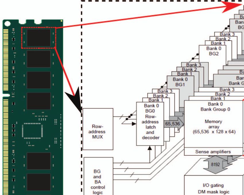
oped cross layer framework (entitled SEAT - System bench- paper, we use Micron 4Gib DDR4 x8 MT40A512M8 @2133
marking for Enablement of Advanced Technologies) allows MHz chip as an example and the baseline design [9]. The
us to carefully validate the feasibility of proposals across the chip configuration is 512 Meg x 8. Since each chip can only
different layers of abstraction (from the device to the system provide 8-bit (8b) data (so-called 8 device), eight chips are
and applications). This is a much more realistic approach organized in a single rank to satisfy the total bus width of
due to the uniformity of the process and silicon validated 64-bit (64b). For the DIMM, we utlize the DDR4 SDRAM
simulation checks at multiple levels. RDIMM (Registered DIMM). Inside one chip, 16 internal
banks are deployed as DRAM cell arrays (bank groups of 4
II. S TATE OF THE A RT by 4 for x4 and x8). A bank can be accessed independently so
Very few studies thoroughly and conclusively analyze the that bank level parallelism is extensively exploited to assure
suitability of STT-MRAM for main memory. Meza et al. memory bandwidth.
[5] analyze architectural changes to enable small row buffers In our case, each bank has 64K rows and 1K columns. If
in NVMs and concludes that NVM main memories with each row contains 1K (1,024) column address staring points
reduced row buffer size can achieve up to 67% energy gain and each column stores 8 bits (1 byte), this would mean
over DRAM at a cost of some performance degradation. each row (page) is 8,192 bits (1,024 x 8 bits) or 1K bytes
Kultursay et al. [6] evaluate STT-MRAM as a main memory per bank. It should be noted that each page of memory is
for SPEC CPU2006 workloads and show that, without any segmented evenly across Bank n of each IC for the associated
optimizations, early-design STT-MRAM is not competitive rank. The DDR4 SDRAM uses an 8n-prefetch architecture
with DRAM. The authors also propose partial write and write to achieve high-speed operation. The 8n-prefetch architecture
bypass optimizations in the STT-MRAM main memory that is combined with an interface designed to transfer two data
achieves performance comparable to DRAM while reducing words per clock cycle at the I/O pins. A single READ or
memory energy consumption by 60%. WRITE operation for the DDR4 SDRAM consists of a single
K Rho et al. [7] propose a 4Gb STT-MRAM, featuring a 8n-bit wide, four-clock data transfer at the internal DRAM
compact 9F2-cell that was developed using advanced technol- core and two corresponding n-bit wide, one-half-clock-cycle
ogy (with the DRAM transistor). The 9090nm2 STT-MRAM data transfers at the I/O pins. Even though we focus on the
was realized by using a compact gate pitch for the wordline, commercial DDR4 in this work, this breakdown and other
and an even finer metal-0 pitch for the bitline and source line. NVM substitutions with the DRAM interface can be easily
The pMTJ process is used here, due to its low switching extended to other DRAM technologies that have similar hierar-
current and high TMR. The 4Gb STTMRAM is not only chy, such as low-power DDR (LPDDR) or 3D-stacked DRAM
based on a compact cell technology, but also employs a high- (e.g., Wide I/O, Hybrid Memory Cube). The DRAM controller
density chip architecture and circuit techniques to maximize is assumed to run at 1GHz. Vdd supply voltage is 1.2V +/-
array density. Kazi et al. [8] conduct a preliminary assessment 60mV and Vpp for wordline boost is 2.5V, 125mV/+250mV.
of HPC system performance impact with STT-MRAM main The chip has a cycle time of 0.937ns @ CL = 16/15. The
memory based on industry estimates and perform a sensitivity random access latency is thus around 42-45ns.
analysis that correlates overall system slowdown trend with To evaluate the DRAM power consumption, we utilize Mi-
respect to average device latency due to unavailability of crons DDR4 power calculator along with our study on DRAM
reliable timing info. Their results demonstrate that the overall internal architecture. Figure 2 shows the power breakdown.
system performance of large HPC clusters is not particularly The power breakdown in Figure 2 can be classified into 3 cat-
sensitive to main-memory latency. Therefore, STT-MRAM, egories : (1) Background Power. The background power takes
as well as any other emerging non-volatile memories with up 28.6% of total power that accounts for the static power
comparable density and access time, can be a viable option and refresh power, which consists of the powers from ACT-
for future HPC memory system design. STBY (active standby), PRE-STBY (precharged standby),
’ACT-PDN’ (active powerdown), PRE-PDN (precharged pow-
III. P OWER B REAKDOWN
erdown) and REF (refresh). (2) RD/WR/Termination Power.3
A. DRAM About 43.5% of the power comes from RD/WR/Termination
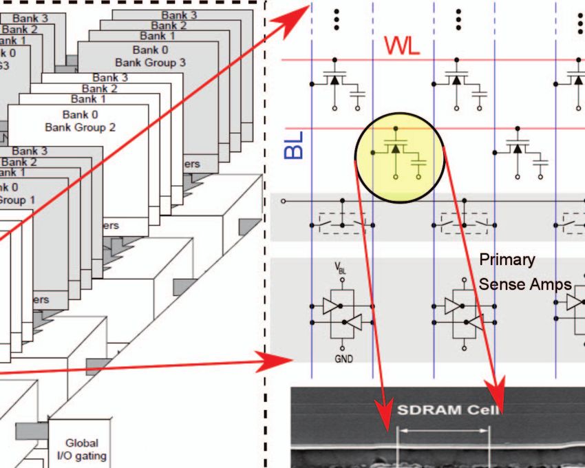
The commercially available DRAM system has a top-down which represents the power for the data movement, including
hierarchical structure, that consists of the DRAM controller, the powers from RD (read burst), WR (write burst), READ
channel, rank, chip, bank as shown in Figure 1. A channel I/O (read bus driver), and Write ODT (write signal on-die ter-
is usually composed of a controller, DIMM/s and a few ranks mination). (3) Activation Power. This consists of 26.9% of the
that share the same command/address and data bus. As the I/O DRAM power. Considerable prior work has been proposed to
data width of a single memory chip is limited, multiple chips reduce the Background Power or RD/WR/Termination Power.
are populated in a rank and operate in lockstep to feed a wider
data bus. The term rank was created and defined by JEDEC B. NVM Main Memory
and refers to a data block that is 64 bits wide. On systems We consider three different alternative main memory so-
that support Error Correction Code (ECC) an additional 8 bits lutions in this paper. Our first proposal consists of a bit-
are added, which makes the data block 72 bits wide. In this cell with the high performance p-MTJ stack was developed
104 Design, Automation And Test in Europe (DATE 2018)
Fig. 1. DRAM internals

on 300mm Si wafers internally. The pMTJ stacks comprise             assumed to be 30 aF/cell. These values are typical of parasitic
of dual MgO interfaces interspersed by magnetic CoFeB               parameters in crossbar arrays using 25-nm technology. The
electrodes, to improve the interfacial Perpendicular Magnetic       STT-MTJ parameters in this proposals are as follows: TMR
Anisotropy (PMA). The free layer (FL) and reference layer           of approximately 110% and a parallel resistance (RP) was 25
(RL) consist of CoFeB-based multilayer stacks. The RL is            kOhm for the dimensions of 30 30 nm2 . Presently, since
coupled to a Co/Pt-based hard layer (HL) to form a synthetic        selector technology is not fully optimized, the higher leakage
anti-ferromagnet (iSAF), this allow us to keep our offset field     contribution compared to conventional transistor options can
near zero. The TMR is around 150% along with a resistance-          lead to an increase in background power. The random access
area (RA) product (7 Ωμm2 ) from the CIPT measurement               latency here is 40ns. The power breakdown profile in Figure 2
and the MTJ pillar dimension is 25nm. Here, we utilize the          alludes to this. Thus, while the 3rd proposal has the smallest
conventional planar transistor as a selector. This results in a     unit area and will be the most cost competitive, it will also be
unit area of 14F2 . Vdd supply voltage is taken to be 0.9V.         the most power hungry option.
The sense amplifier is enabled when the difference between
the reference and the cell read out reaches around 70mV. The
drawback here is that the unit cell area of STT-MRAM is still
much larger than that of DRAM, making STT-MRAM not
cost-competitive to contemporary DRAM. The random access
latency here is 30ns.
   The second proposal borrows from [7]. Two different supply
voltages are present here to help boost the WL and compensate
for the weak DRAM transistor (Vdd 1 = 1.2V and Vdd 2 = 1.8V).
The chip operation is similar to that of mobile LPDDR2-
S4B DRAM, resulting in a random read latency of 50ns. This
chip is however about 1.4 times smaller than the previous
proposal. The third and the final proposal involves the use of
a highly nonlinear bi-directional selector device that opens up
                                                                    Fig. 2. A comparative power breakdown of the different Main memory
the possibility of the stacking to reduce the unit area and be      solutions.
cost competitive with contemporary DRAM [10]. This results
in a unit area of 4F2 . The drain voltages of selected WL/BL
driving transistors are 1.8/0 V, and the gate voltage of selected                  IV. S YSTEM LEVEL A NALYSIS
WL/BL driving transistors is 3.3 V. The line resistance was           The system level analysis is carried out by combining
assumed to be 2 Ohm/sq, and the parasitic capacitance was           two modeling and simulation tools: gem5 [11] and NVMain

                                    Design, Automation And Test in Europe (DATE 2018)                                             105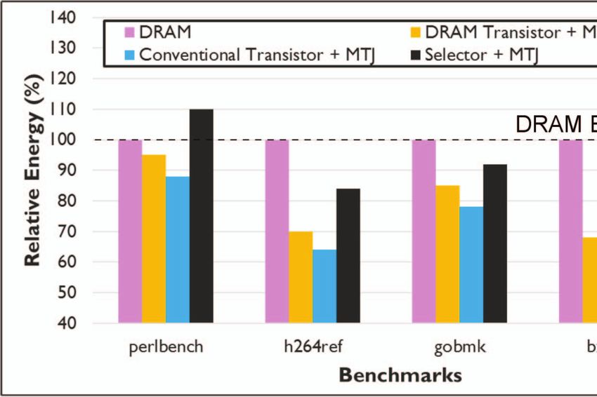
[12]. From input parameters characterizing a given system         method. Then, the corresponding pkt is retrieved from the
configuration, these tools are co-simulated in order to produce   map data structure and sent back to gem5 as part of the
execution statistics including execution time, memory transac-    request completed confirmation through the sendTimingResp
tions and related latencies, power/energy consumption.            method, which is triggered by a RespondEvent (previously
   The gem5 computer architecture simulator [11] provides         scheduled in the gem5 event queue by the interfacing object).
an accurate evaluation of system performance thanks to its        Furthermore, the NVMainMemory interfacing object and the
high configurability for a fine grained architecture modeling.    NVMain simulator are cycled every clock cycle through the
Its full-system simulation mode runs unmodified operating         tick method, which propagates the standard gem5 cycling to
systems. It has been used for the accurate modeling and           NVMain through the Cycle method.
evaluation of modern multicore architectures, such as ARM
                                                                  B. Framework soundness evaluation
big.LITTLE [13]. NVMain [12] is an architectural-level sim-
ulator that enables to model main memory design with both            Experiments have been carried out to evaluate the correct-
DRAM and emerging non-volatile memory technologies. It is         ness of gem5-NVMain framework by considering a set of
well-integrated together with the gem5 simulator, which makes     relevant applications (from the SPEC CPU2006 benchmark
it possible to achieve cycle-approximate multicore system         suite [14]) running on a system with the aforementioned
simulation together with cycle-level simulation of a variety      Micron 4Gib DDR4 x8 MT40A512M8 @2133 MHz main
of main memory technologies in the system. In addition,           memory baseline design. The experimental setup is detailed in
NVMain can also accommodate traces as input for facilitating      Table I. An important motivation of this evaluation framework
design space exploration by considering either user-defined
emerging memory technologies or those provided together                                             TABLE I
                                                                                          A RCHITECTURE CONFIGURATION
with the simulator. In this paper, we consider both options by
calibrating a few DRAM models based on available datasheets.         System element                         Configuration
   A given memory configuration in NVMain is described                                                      64-bit RISC ARMv8
by several tens of parameters regarding the corresponding               Processor                         single core, out-of-order
                                                                                                                    2GHz
architecture for which a template is illustrated in Figure 3,      L1 Instruction cache                         Private, 64kB
and its timing and energy consumption. These parameters are          L1 Data cache                              Private, 64kB
leveraged by during the co-simulation NVMain to estimate                L2 cache                                Shared, 1M B
                                                                                                                  2 channels
the delay and energy consumption of the main memory in the
                                                                                                             2 ranks per channel
execution of a particular workload. For available memories,           Main Memory                              8 chips per rank
these configuration parameters are gathered from datasheet                                              Memory controller at 1GHz
                                                                                            Micron 4Gib DDR4 x8 MT40A512M8 @2133 MHz chip
information and are very accurate.
A. gem5-NVMain co-simulation                                      is to enable a rapid design space exploration while integrating
   In order to obtain a good simulation accuracy, gem5 and        NVMs into main memory. For this reason, our first experiment
NVMain need a tight interaction. NVMain receives memory           focuses on the relevance assessment of gem5 system call
requests from gem5 at precise time instants; these requests       emulation (SE) and full system (FS) simulation modes. The SE
should trigger different NVMain actions (i.e., request en-        mode is used to simulate individual applications without the
queueing, scheduling, transfer to main memory, bank latency       need to model devices or an operating system (OS). System
computation and transfer back to controller) that need to be      calls are emulated by calling the host OS, enabling a fast
executed (to preserve dependencies) before gem5 can proceed       simulation. On the other hand, FS mode executes both user-
with its simulation. Accordingly, gem5 and NVMain have been       level and kernel-level instructions and models a complete
integrated (by NVMain developers) in the co-simulation envi-      system including the OS and devices. This includes support
ronment illustrated in Figure 4 as part as the used framework.    for interrupts, exceptions, privilege levels, and I/O devices. For
   An interfacing object, namely NVMainMemory, is created         illustration, Table II summarizes an evaluation of the perlbench
inheriting from both, the AbstractMemory gem5 class and           application in both SE and FS mode combined with NVMain.
the NVMObject NVMain class. As a gem5 object, the newly
created interfacing object can respond to the recvTimingReq                                    TABLE II
method triggered by the last level cache during the gem5                 S YSTEM C ALL E MULATION VS F ULL S YSTEM S IMULATION
simulation. Each received request includes a gem5 memory                                   Parameter             SE         FS
request packet, namely pkt, whose information is transferred                          Runtime (second)          0.006      0.0104
onto a new NVMain memory request packet, namely req, that                         Main memory reads (kilo)        17         21
is then submitted to the NVMain simulator. To keep track of                       Main memory writes (kilo)       2          43
                                                                                Main memory bandwidth (MB/s)     205         400
the issued memory requests, the interfacing object stores both
the pkt and the corresponding req in a map data structure. Once
NVMain has completed the submitted memory operation, the             The SE mode estimates an execution time of 0.006 seconds,
interfacing object is notified through the RequestCompleted       instead, the FS simulation estimates 0.0104 seconds. The time

106                                   Design, Automation And Test in Europe (DATE 2018)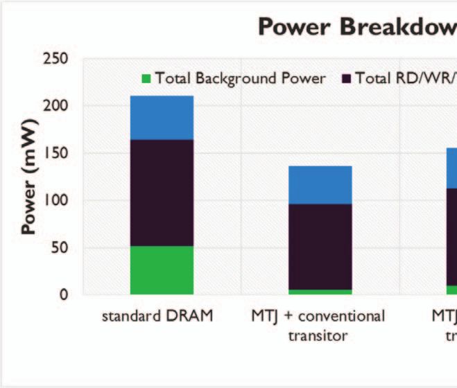
Chip#0 Device
width
Rows
Channel#1 Mem Mem bus Rank#0 ...
contr#1 width Bank#0
... Chip#c
Mem Channel#0 ... Bank#1
contr#0 Row buffer
Channel#c Mem ...
contr#c
Rank#r Bank#b
ARMv8 chip
Fig. 3. NVMain memory architecture template that needs to be instantiated in the configuration files.
! ! %%
$ !
!%
$
!() $()
#
$
$
!
!
!
$
#
!
! !
&
!
() # #
" !'
*
#! ""
Fig. 4. Software architecture of the gem5/NVMain co-simulation.
difference comes from the fact that SE does not amount for is indicated by the row buffer hits/misses values. Obviously,
the time spent by the architecture in the handling of OS an execution optimised for minimal main memory latency
system calls. However, such events are important to consider will aim at minimising the more expensive row buffer misses.
when evaluating a particular memory architecture. The number The total main memory access latency is split between aver-
of memory reads and writes to main memory can differ age memory access latency and average queue latency. The
by an order of magnitude between the FS and SE mode. latter is the average time a memory request spends in the
Alternative fast gem5 simulation approaches such as [15] memory queue waiting to be served. Finally, one can also
could be rather considered. Now, let us consider the gem5 FS observe how often the memory simulation was triggered by
mode together with NVMain in order to evaluate the accuracy comparing the wakeupCount with respect to the total number
of the framework compared to the main memory design ref- of simulation cycles. Another experiment has been conducted
erence (i.e. Micron DDR4). A set of system activity statistics with 12 applications of the PARSEC 3.0 benchmark suite [16]
are collected through Table III, based on the execution of demonstrating that NVMain rarely accounts for more than
the SPEC CPU2006 perlbench, h264ref, gobmk and bzip2 15% of the overall simulation time (Figure 5, right). Moreover,
applications. it is observed that the NVMain contribution on the total sim-
ulation time is not correlated to the main memory bandwidth
TABLE III (Figure 5). Among all the simulated PARSEC applications,
M AIN MEMORY STATISTICS the simulation time varies from about 4 to 36 hours. Each
Parameter perlbench h264ref gobmk bzip2
simulation traces consider a minimum of 1, 500, 00 samples
Main memory reads 1.13e6 5.24e7 4.32e7 9.51e7 which corresponds to about a 4-hour execution time.
Main memory writes 8.42e5 2.78e7 4.11e7 4.48e7
Row buffer hits 5.66e5 2.96e7 4.84e7 1.67e7 V. C OMPARATIVE S YSTEM LEVEL A NALYSIS AND
Row buffer misses 1.41e6 5.06e7 3.59e7 1.23e8 C ONCLUSION
Average latency (ns) 51.64 50.2 42.28 56.46
Average queue latency (ns) 10.4 12.19 35.88 1.79
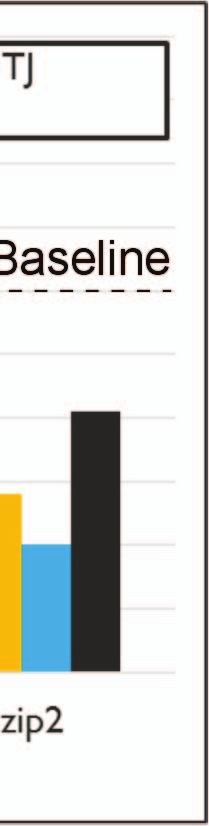
Figure 6 highlights a relative comparison between the
Average total latency (ns) 62.04 62.39 78.15 58.25 different NVM main memory solutions and DRAM from a
Simulation cycles 1.31e10 1.88e10 2.49e10 1.26e10 system energy consumption point of view. From the graphs
Wakeup count 3.03e7 4.16e8 3.82e8 7.09e8
it is quite clear that the NVM solutions fare better than
the DRAM almost every-time. It is only when the write
The row buffer locality exploited by the memory controller access dominates the benchmark/application suite that the
Design, Automation And Test in Europe (DATE 2018) 107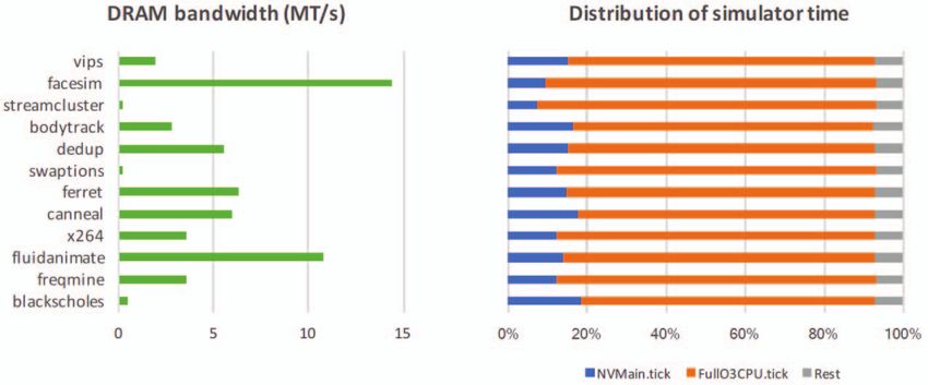
Fig. 5. DRAM bandwidth and Full System simulation time breakdown.

NVM energy consumption shoots up. This can be attributed                                             R EFERENCES
to the higher write energy of MRAM compared to DRAM                     [1] Q. Deng, L. Ramos, R. Bianchini, D. Meisner, and T. Wenisch, “Active
and it’s own read (asymmetric nature). The high resistance                  low-power modes for main memory with memscale,” IEEE Micro,
MTJ cells in ‘MTJ + Selector’ option leads to increased                     vol. 32, no. 3, pp. 60–69, May 2012.
                                                                        [2] S. Li, P. Chi, J. Zhao, K. T. Cheng, and Y. Xie, “Leveraging nonvolatility
RC delay and thus longer access times. This combined with                   for architecture design with emerging nvm,” in IEEE NVMSA, Aug 2015,
the higher voltage requirements due to the immaturity of the                pp. 1–5.
selector technology leads to the relatively higher energy energy        [3] Y. Xie, “Modeling, architecture, and applications for emerging memory
                                                                            technologies,” IEEE Design Test of Computers, vol. 28, no. 1, pp. 44–51,
consumption (only 8% average energy reduction across the                    Jan 2011.
different benchmarks compared to conventional DRAM). The                [4] D. Apalkov et al., “Spin-transfer torque magnetic random access mem-
‘MTJ + selector’ option will be most viable in the future if                ory (stt-mram),” J. Emerg. Technol. Comput. Syst., vol. 9, no. 2, pp.
                                                                            13:1–13:35, May 2013.
and when the selector is optimized for leakage and dynamic              [5] J. Meza, J. Li, and O. Mutlu, “Evaluating row buffer locality in future
power. While, the ‘MTJ + conventional transistor’ is the most               nonvolatile main memories,” Carnegie Mellon University, IBM Watson
energy efficient among the NVM proposals (27% average                       Research Center, Tech. Rep. SAFARI Technical Report No. 2012-002,
                                                                            12 2017.
energy reduction across the different benchmarks compared               [6] E. Kltrsay, M. Kandemir, A. Sivasubramaniam, and O. Mutlu, “Evalu-
to conventional DRAM), it is also the least cost effective due              ating stt-ram as an energy-efficient main memory alternative,” in IEEE
to the large cell size (more than 2 times that of DRAM).                    ISPASS, April 2013, pp. 256–267.
                                                                        [7] K. Rho et al., “23.5 a 4gb lpddr2 stt-mram with compact 9f2 1t1mtj
Finally, it must be mentioned that while we assume a DRAM                   cell and hierarchical bitline architecture,” in 2017 IEEE International
like interface for these NVM proposals, the full benefits                   Solid-State Circuits Conference (ISSCC), Feb 2017, pp. 396–397.
of NVMs can only be leveraged through micro-architectural               [8] K. Asifuzzaman et al., “Performance impact of a slower main memory:
                                                                            A case study of stt-mram in hpc,” in MEMSYS. New York, NY, USA:
modifications and custom interfaces that maximize the benefits              ACM, 2016, pp. 40–49.
of NVMs.                                                                [9] “4gb ddr4 sdram,” Micron Technology inc., Tech. Rep. 4gb ddr4
                                                                            dram.pdf - Rev. H 5/17 EN, 2012.
                                                                       [10] H. Lim, S. Lee, and H. Shin, “Switching time and stability evaluation
                                                                            for writing operation of stt-mram crossbar array,” IEEE Transactions on
                                                                            Electron Devices, vol. 63, no. 10, pp. 3914–3921, Oct 2016.
                                                                       [11] N. Binkert et al., “The gem5 simulator,” SIGARCH Comput. Archit.
                                                                            News, vol. 39, no. 2, pp. 1–7, Aug. 2011.
                                                                       [12] M. Poremba, T. Zhang, and Y. Xie, “Nvmain 2.0: A user-friendly
                                                                            memory simulator to model (non-)volatile memory systems,” IEEE
                                                                            Computer Architecture Letters, vol. 14, no. 2, pp. 140–143, July 2015.
                                                                       [13] A. Butko, F. Bruguier, A. Gamati, G. Sassatelli, D. Novo, L. Torres, and
                                                                            M. Robert, “Full-system simulation of big.little multicore architecture
                                                                            for performance and energy exploration,” in 2016 IEEE MCSOC, Sept
                                                                            2016, pp. 201–208.
                                                                       [14] J. L. Henning, “Spec cpu2006 benchmark descriptions,” SIGARCH
                                                                            Comput. Archit. News, vol. 34, no. 4, pp. 1–17, Sep. 2006. [Online].
                                                                            Available: http://doi.acm.org/10.1145/1186736.1186737
                                                                       [15] A. Butko, R. Garibotti, L. Ost, V. Lapotre, A. Gamatie, G. Sassatelli,
                                                                            and C. Adeniyi-Jones, “A trace-driven approach for fast and accurate
                                                                            simulation of manycore architectures,” in ASPDAC, Jan 2015, pp. 707–
                                                                            712.
Fig. 6. The relative energy consumption of the NVM based main memory   [16] C. Bienia, S. Kumar, J. P. Singh, and K. Li, “The parsec benchmark
solutions and conventional DRAM                                             suite: Characterization and architectural implications,” in PACT. New
                                                                            York, NY, USA: ACM, 2008, pp. 72–81.

108                                       Design, Automation And Test in Europe (DATE 2018)
You can also read