Multiplexing Control Circuit and Improved Pulse Analysis for Kinetic Inductance Detectors
←
→
Page content transcription
If your browser does not render page correctly, please read the page content below
Multiplexing Control Circuit and
Improved Pulse Analysis for Kinetic
      Inductance Detectors

                       Jacob Miller

     A Bachelors Thesis presented in partial satisfaction of the
                   requirements for the degree of
                        Bachelor of Science
                                 in
                              Physics

                    College of Creative Studies
              University of California, Santa Barbara
                             June 2021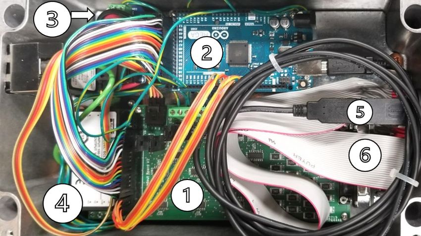
The Bachelors Thesis of Jacob Miller is approved.

           Professor Benjamin Mazin

                   June 2021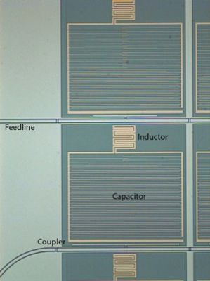
Acknowledgements

I want to give huge thanks to my research advisor, Professor Benjamin Mazin and my
graduate student mentor, Nicholas Zobrist for working with me over the last three years. I
have come a long way as a scientist and I am tremendously grateful for their guidance. I am
also thankful for all of the other members of the Mazin Lab for being extremely generous
in offering me assistance in my research and support and encouragement through my first
experiences presenting scientific talks and posters.
   I would also like to thank the College of Creative Studies (CCS) and donors of the
CCS Create Fund Summer Fellowship for funding my work on the PMM control circuit.
I want to recognize Nicholas Zobrist who began the work on the PMM project before I
joined the project and Bruce Bumble who is developing the PMM arrays at NASA’s Jet
Propulsion Laboratory. I finally want to express appreciation towards the Eddleman Center
for Quantum Innovation at UCSB and Roy T. Eddleman for supporting my research on KID
pulse analysis through the Eddleman Fellowship.

                                              1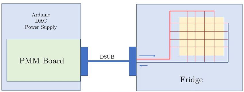
Contents

1 Introduction                                                                                   5

2 Programmable Magnetic Multiplexing (PMM) Array                                                 8
  2.1   Tuning Resonator Frequencies . . . . . . . . . . . . . . . . . . . . . . . . . .        10
  2.2   Programmable Magnetic Array . . . . . . . . . . . . . . . . . . . . . . . . .           10
  2.3   Row-Column Multiplexing . . . . . . . . . . . . . . . . . . . . . . . . . . . .         11
  2.4   Control Circuit . . . . . . . . . . . . . . . . . . . . . . . . . . . . . . . . . .     12

3 PMM Unit Design                                                                               16
  3.1   Setting Currents    . . . . . . . . . . . . . . . . . . . . . . . . . . . . . . . . .   17
  3.2   Circuit Design and Board Routing . . . . . . . . . . . . . . . . . . . . . . . .        18
  3.3   Circuit Fabrication and Unit Assembly . . . . . . . . . . . . . . . . . . . . .         20
  3.4   Control Software . . . . . . . . . . . . . . . . . . . . . . . . . . . . . . . . .      22

4 PMM Unit Characterization                                                                     23
  4.1   Voltage Setting . . . . . . . . . . . . . . . . . . . . . . . . . . . . . . . . . .     23
  4.2   Current Measurement . . . . . . . . . . . . . . . . . . . . . . . . . . . . . . .       24
        4.2.1   Voltage Bias . . . . . . . . . . . . . . . . . . . . . . . . . . . . . . . .    24
        4.2.2   Gain . . . . . . . . . . . . . . . . . . . . . . . . . . . . . . . . . . . .    25
  4.3   Current Setting . . . . . . . . . . . . . . . . . . . . . . . . . . . . . . . . . .     26
        4.3.1   Linearity with Voltage . . . . . . . . . . . . . . . . . . . . . . . . . .      26
        4.3.2   Accuracy    . . . . . . . . . . . . . . . . . . . . . . . . . . . . . . . . .   27
        4.3.3   Max Currents . . . . . . . . . . . . . . . . . . . . . . . . . . . . . . .      27
  4.4   Row and Column Resistors . . . . . . . . . . . . . . . . . . . . . . . . . . . .        28

                                               2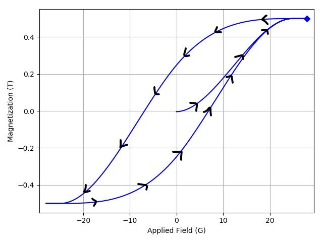
CONTENTS

  4.5   Reset Function . . . . . . . . . . . . . . . . . . . . . . . . . . . . . . . . . .    30

5 PMM Simulation                                                                              31
  5.1   Modeling Hysteresis . . . . . . . . . . . . . . . . . . . . . . . . . . . . . . . .   31
  5.2   Modeling Resonator Response . . . . . . . . . . . . . . . . . . . . . . . . . .       33
  5.3   Resonator Tuning . . . . . . . . . . . . . . . . . . . . . . . . . . . . . . . . .    34

A Improving Energy Resolution                                                                 38

                                               3
List of Figures
1.1 Image of a Microwave Kinetic Inductance Detector (MKID) . . . . . . . . . 6
2.1 Example frequency response of an MKID array . . . . . . . . . . . . . . . . 9
2.2 SEM images of Programmable Magnetic Multiplexed (PMM) array . . . . . 11
2.3 PMM control unit schematic . . . . . . . . . . . . . . . . . . . . . . . . . . . 12
2.4 Magnitude switching function for the PMM control circuit current output . . 13
2.5 Sign switching function for the PMM control circuit current output . . . . . 14
3.1 Amplification and current buffering circuit schematics . . . . . . . . . . . . . 17
3.2 Routed PMM control circuit layout . . . . . . . . . . . . . . . . . . . . . . . 19
3.3 Reflow soldering process for surface-mounted components . . . . . . . . . . . 21
3.4 Complete PMM control unit . . . . . . . . . . . . . . . . . . . . . . . . . . . 21
4.1 Calibration curve for DAC error . . . . . . . . . . . . . . . . . . . . . . . . . 24
4.2 Characterization of DAC error before and after calibration . . . . . . . . . . 25
4.3 Calibrating sense resistance of current-sense IC . . . . . . . . . . . . . . . . 26
4.4 Current setting measurements for control circuit . . . . . . . . . . . . . . . . 27
4.5 Error measurement of current-setting using control circuit . . . . . . . . . . 28
4.6 Row/column maximum currents . . . . . . . . . . . . . . . . . . . . . . . . . 29
4.7 Oscilloscope capture of reset function for magnets . . . . . . . . . . . . . . . 30
5.1 Example hysteresis curve modeled using Preisach model . . . . . . . . . . . . 32
4Chapter 1
Introduction
Microwave Kinetic Inductance Detectors (MKIDs) are microscopic superconducting sensors
that are used for highly sensitive astronomical observing. MKIDs work by utilizing a quan-
tum effect occurring in superconductors called the kinetic inductance effect, which is respon-
sible for changing the surface impedance of the superconductor upon photon incidence (more
detail in [8]). For each detector, the superconductor is patterned into a microwave resonator
(Fig 1.1) which has a frequency response that varies with changing surface impedance. De-
tectors can be multiplexed into arrays by fabricating each detector with a unique resonant
frequency and addressing it at that frequency on a common feedline. This scheme reduces
the wires into the superconducting stage of the fridge and allows for realization of arrays
with thousands of detectors [7, 9, 12].
Superconducting technologies are ideal for astronomical observing because they are not
limited by the read noise which is present in semiconductor technologies and are therefore
highly sensitive to dim or distant sources of light. MKIDs and Transition Edge Sensors
(TESs) are currently the dominant superconducting detector technologies and each are able
to detect signals from single photon impacts. TES devices operate by detecting photon-
induced phase transitions out of the superconducting phase which appear as a change in DC
current through the sensor. Both MKID and TES arrays are well-suited for ground-based
operation because their ultra-fast readout systems allow them to work well with adaptive
optics and speckle nulling [1].
The most significant trade-off between MKID and TES technologies is between their
5CHAPTER 1. INTRODUCTION
Figure 1.1: Image of a Microwave Kinetic Inductance Detector (MKID) with the capacitor
and inductor labeled.
spatial and spectral resolutions. The spatial resolution of a detector array is the number of
detectors than can be fabricated and operated in a single array. In most cases the spatial res-
olution for MKID and TES arrays is not limited by their physical spacing, but instead by data
transport out of the superconducting refrigeration stage. Each additional wire contributes
heat to the fridge and too many wires can render it impossible to reach superconducting
temperatures. MKIDs have an advantage in this domain because they are compatible with
frequency-multiplexing schemes that allow for the readout of many detectors, or resonators,
per wire. Creating higher pixel-count MKID arrays is therefor an issue of fitting more res-
onators within a single frequency bandwidth. Chapters 2-5 discuss research into a method for
improving the spatial resolution of MKID arrays by tuning resonant frequencies of individual
detectors.
Although MKIDs are relatively easier to multiplex and therefor offer better spatial reso-
lutions, TES devices in general achieve a better spectral resolution. The spectral resolution
of a detector is the precision with which it can measure the energy of an incident photon
and is important when studying the emission spectrum of a light source. Improved spectral
resolution is especially important for optical MKIDs in the study of planets orbiting distant
stars [10] where a planet’s emission spectrum is used to determine its atmospheric composi-
6CHAPTER 1. INTRODUCTION
tion. We wish to improve the spectral resolution of MKIDs to achieve a detector technology
that is capable of both high spatial resolution and precise energy measurements (discussed
further in [13]). Improvements to spectral resolution for MKIDs are being pursued in two
main areas: detector physics [11, 14] and data processing. One direction of research that
explores improving the spectral resolution of MKIDs and thermal KIDs (TKIDs) through
new data processing methods is discussed in Appendix A.
7Chapter 2
Programmable Magnetic Multiplexing
(PMM) Array
The spatial resolution of a MKID array is primarily limited by two factors: the number of
pixels that can be fabricated on the physical detector, and the number of unique resonator
frequencies that can fit within the readout bandwidth. The work presented in this thesis
explores a remedy to the second limitation. As we add more resonators to the physical
detector array, the frequency bandwidth of our readout grows because each resonator has a
finite width in frequency space. An example frequency response curve is shown in Fig 2.1
where each valley represents a resonator and each valley’s width is set by the resonator’s
linewidth. We encounter an eventual limit to the number of pixels in a single array because
the cost of room-temperature readout electronics scales with frequency bandwidth (∼ GHz in
existing systems). To maximize pixel count within a limited bandwidth, resonator frequencies
are placed as close together as possible.
The “hard limit” of pixel density in frequency space is set by the line width of the res-
onators. However, our primary consideration when spacing resonator frequencies is instead
the tolerance with which we can place resonators in frequency space. The valley of a res-
onator’s frequency response is centered at the circuit’s resonant frequency, which is set by
√
ω0 = 1/ LC. Precision in resonator frequency placement is therefor limited by the preci-
sion with which we can set the resonator’s inductance and capacitance in fabrication. This
8CHAPTER 2. PROGRAMMABLE MAGNETIC MULTIPLEXING (PMM) ARRAY
Figure 2.1: Example frequency response of an MKID array where power transmission is
plotted as a function of signal frequency. The array is probed with many tone frequencies
and the response for each frequency is measured. The valleys (upside down spikes) marked
in green represent the resonant frequency of a single resonator in the array.
fabrication tolerance can be on the order of several linewidths and is accentuated by mate-
rial imperfections which contribute a further placement error with large variance. Placing
resonator frequencies with separation comparable to the magnitude of this variance would
require large spacing and result in extremely low detector pixel count.
The trade-off that we settle for is close (but not minimal) spacing at the cost of some
fraction of the resonators being erroneously placed out-of-order in frequency space. This
trade-off results in two cases of misplaced resonators: swapped resonators and overlapped
resonators. A swapped resonator occurs when placement error is large enough that a valley is
placed on the opposite side of a neighboring valley such that their order is swapped. In some
cases, the error is large enough that the resonator is placed several neighboring valleys away.
Swapped resonators are only usable once their valleys are located using a lengthy process of
probing each pixel on the physical detector. An overlapped resonator occurs if two valleys
are placed such that they respond to the same frequencies. If the overlap is significant, these
pixels are indiscernible and both become unusable.
9CHAPTER 2. PROGRAMMABLE MAGNETIC MULTIPLEXING (PMM) ARRAY
2.1 Tuning Resonator Frequencies
We propose that the ability to tune the resonant frequency of each physical pixel post-
fabrication would help alleviate existing limitations which include the high cost of readout
electronics due to non-optimal resonator spacing, the decreased pixel yield due to misplaced
resonant frequencies, and the time-consuming process for manually locating swapped res-
onators.
By shifting a resonator’s valley in frequency space, overlapping pixels could be resolved,
which would in turn allow for a closer packing of resonators in general without having to
worry about losing pixels to overlap. We project that these improvements to pixel yield
and resonator packing could lead to an increase in the pixel yield of a MKID readout by
a factor of four or more. In addition, a computer-controlled method for tuning resonant
frequencies could be used as an automated method for locating pixels in frequency space
that have potentially been swapped. By shifting the resonant frequency of each physical
pixel and reading out the array’s frequency response, a map of a pixel’s physical coordinates
to its frequency could be generated autonomously. This would dramatically reduce the time
and resources required to calibrate an array.
2.2 Programmable Magnetic Array
It has been shown that magnetic field penetration through superconducting resonators af-
fects loss mechanisms within the superconductor and thus changes the resonant frequency of
the circuit [3, 2, 5]. Extending on these results, the Mazin Lab at UCSB has been working
on developing a new approach for tunable magnetic penetration of superconducting MKID
resonators using a nearby array of programmable micro-magnets. The programmable mag-
netic multiplexing (PMM) array is a grid of ferromagnets (pictured in Fig 2.2a) that will
be placed underneath a MKID array with one magnet per pixel. Each magnet (pictured in
Fig 2.2b) contains an embedded loop of current-carrying wire that acts as an electromagnet.
The magnetization at each location can be set by sending current through the electromagnet
and will be remembered due to the hysteretic properties of the ferromagnet.
10CHAPTER 2. PROGRAMMABLE MAGNETIC MULTIPLEXING (PMM) ARRAY
(a) Array of Magnets (b) Single Magnet
Figure 2.2: The Programmable Magnetic Multiplexed Array consists of a grid (a) of ferro-
magnets (b) that can each be magnetized by an accompanying electromagnet. The electro-
magnets are controlled by currents that flow down each row and column of the array. These
SEM images were taken by Bruce Bumble at JPL.
Tuning the frequency of each resonator using the PMM array requires control of the
magnetic field through each pixel, which in turn requires control of the current through each
electromagnet in the array. For an array of order N ∼ 104 pixels, it is not feasible to address
each electromagnet with its own control wire. Doing so would require ∼ 104 wires to go
from room temperature control electronics into the superconducting stage of the fridge. To
alleviate this problem, we propose a row-column multiplexing scheme requiring only ∼ 102
wires in which current is controlled only through each row and column of the array. Using
this scheme, the current through the electromagnet at a site with coordinate (i, j) will be
(i) (j)
set by I (i,j) = Irow + Icol .
2.3 Row-Column Multiplexing
Using row-column multiplexing, a current of I through site (i, j) is achieved by sending
a current of I/2 through the ith row and a current of I/2 through the jth column. To
minimize the current through all other junctions, a reverse current of −I/6 is sent through
all other rows and columns. With this configuration, the site at (i, j) receives a current with
magnitude I and all other sites receive a reverse current of magnitude I/3.
11CHAPTER 2. PROGRAMMABLE MAGNETIC MULTIPLEXING (PMM) ARRAY
Figure 2.3: Schematic illustration of the PMM control unit. The PMM board includes
current switching a regulation while the digital to analog converter (DAC) provides precise
current control. The Arduino offers a serial connection so that switching can be automated
over USB. The two thicker lines entering and exiting the DSUB at the fridge stage each
represent the eight wires that break out into the rows and columns. Four rows and four
columns are illustrated here for schematic purposes.
The currents can be applied and immediately removed and the resulting magnetization
at each site will be determined by the properties of the hysteresis curve specific to the
ferromagnets used. In general, a ferromagnet will retain a large fraction of its magnetization
when a significant magnetic field (such as at the target site) is applied and removed. It is
also a general property of hysteresis that small fields (such as at all non-target sites) have
little effect on the magnetization when applied and removed. We develop our apparatus so
that the ferromagnets will largely remember their magnetization when pulsed with a field
set by a current I, but will have little memory of the perturbation to their magnetization
due to a field set by a current I/3.
2.4 Control Circuit
The implementation of the PMM control unit is illustrated schematically in Fig 2.3. The
currents through each row and column of the array are controlled by switches on a room-
temperature printed circuit board (PCB). This PCB, an Arduino for serial interface, a digital
to analog converter (DAC) for current control, and a power supply make up the PMM control
unit. The unit is connected to the fridge through a current-carrying interface.
12CHAPTER 2. PROGRAMMABLE MAGNETIC MULTIPLEXING (PMM) ARRAY
Figure 2.4: Schematic illustration of the current magnitude switching function for the PMM
control circuit. Each row and column of the array must be able to receive a current of either
I or I/2 in order to set a current of 2I at the target intersection. To achieve this, we send a
voltage of Vtop = V and Vbottom = −V to each row and column. The switches are configured
so that Vtop drives a larger forward current through Rsmall on a single row or column and
Vbottom drives a smaller reverse current through Rbig on all other rows and columns. This
schematic diagram shows an example array with only four rows and four columns.
To have the capacity for applying a target current of 2I to any intersection, each each row
and column of the array should be able to draw a current of either I or −I/3. This control is
implemented at each row and column by switching between two paths: one with resistance
Rsmall connected to voltage V and another with resistance Rbig connected to voltage −V as
depicted in Fig 2.4. Using this arrangement, the voltage V is always connected to the small
resistor thus generating a large current with direction set by the sign of V . The voltage
−V is always connected to the big resistor which generates a smaller current in the opposite
direction. The resistor values are responsible for setting the ratio of forward current to
reverse current and are chosen such that
Rbig + R0 = C ∗ (Rsmall + R0 ) (2.1)
where R0 is the constant trace/component resistance of the current path and C is our target
ratio of 3. Using this switching configuration, the control circuit requires two single pole
13CHAPTER 2. PROGRAMMABLE MAGNETIC MULTIPLEXING (PMM) ARRAY
Figure 2.5: Schematic illustration of the current sign switching function for the PMM control
circuit. The current is controlled using an input voltage Vin which is amplified and current-
buffered before being delivered to each row and column. Each row and column receives an
voltage amplified with a gain of G as well as a voltage amplified with a gain of −G. In this
example, G = 3. The sign of Vtop and Vbottom can be swapped using the illustrated switches.
single throw (SPST) switches per row and column. None of the switch pairs will ever be
closed at the same time.
The PMM array has the ability to apply both positive and negative magnetic fields to
each target intersection. This functionality is implemented in the control circuit by adding
a switching component (Fig 2.5) to swap the sign of the current-setting voltage V and its
reverse counterpart −V (labeled as Vtop and Vbottom in the figure). The component takes in
a voltage Vin from the DAC and outputs a voltage V = ±3Vin which is used for setting the
currents. The value of V is limited by the positive and negative power supply voltages of
Vs + and Vs −. Switching in this component requires two single pole double throw (SPDT)
switches1 .
The PMM control unit’s input consists of an analog voltage Vin and Ninput single-bit wires
to toggle the switches where
Ninput = 2 + 2(Nrow + Ncol ). (2.2)
The analog voltage is set by a DAC which is controlled over USB using an Arduino data
interface. The Arduino headers are used to control the switches in the case that there are
1
Or an equivalent configuration using SPST switches that is discussed in Section 3.1.
14CHAPTER 2. PROGRAMMABLE MAGNETIC MULTIPLEXING (PMM) ARRAY
few enough rows and columns. For a full-scale version of the PMM control circuit with
Nrow ∼ Ncol ∼ 100, the Arduino will not have adequate header connections and the switches
will instead need to be addressed over a serial interface to the board.
15Chapter 3
PMM Unit Design
The first design of the PMM array is a prototype version with support for current delivery
over only nine rows and ten columns. We control the board using an Arduino Mega 2560
which has 54 digital input/output pins. Of these, 40 pins are used for switching (referring to
Eq 2.2) and two are used as an I2 C serial interface for controlling the AD5667 16-bit DAC.
The 40 switching pins are used as enable wires for 46 SPST switches contained in the 12
surface-mounted DG412DYZ quad switch ICs.
The board is powered using a ±15 V wall-powered (120 V) AC/DC converted which
drives the currents down the rows and columns of the PMM array. The board is designed to
send a max current of ≈ 24.2 mA through the targeted row and column and a corresponding
reverse current of ≈ 6.3 mA through the remaining 17 rows and columns. According to this
specification, the max current draw through the power supply at any time (when the board
is operated properly) is Imax ≈ 6.3 ∗ 17 mA ≈ 110 mA. The power supply has a max current
draw of 150 mA which can support this max operational load of the PMM circuit
The 19 row and column outputs as well as the single current return are wired to a DSUB
interface. The control circuit can be connected to the fridge or any testing apparatus using
a DSUB cable. The control circuit includes a surface-mounted INA213 current-sense circuit
that is connected to the circuit drain. The INA213 outputs an analog voltage which we read
using one of the Arduino’s analog inputs. The ability to measure total current gives us an
avenue for testing, debugging, and calibrating the circuit.
16CHAPTER 3. PMM UNIT DESIGN
(a) Amplifiers (G± = ±3) (b) Current Buffer
Figure 3.1: Voltages on Vtop and Vbottom are set using amplifiers with gain G± = ±3 (a) that
amplify the DAC voltage Vdata . These voltages drive currents through the PMM array so
they are buffered using transistors (b) that draw from the ±15 V power supply of the control
unit.
3.1 Setting Currents
The approximate 3:1 ratio for forward current to reverse current is set using fixed-resistance
surface-mounted resistors with nominal values of 620 Ω and 2400 Ω at each row and column.
Solving Eq 2.1, we find a ratio C = 3.9 for zero trace resistance (R0 = 0) and find that C
gets closer to the target ratio of C = 3 for nonzero R0 . The specific resistors we chose are 1%
tolerance with a maximum power dissipation of 2 W. The power dissipation of the resistors
is important because they need to support large currents. With a maximum driving voltage
of 15V we will need to dissipate up to P = (15V )2 /(620 Ω) = 363 mW, so 1/8 W resistors
are insufficient.
The magnitudes of the current-setting voltages Vtop = +V and Vbottom = −V are set
using a voltage Vdata that is supplied by the DAC with a range of 0V to 5V. The voltage
Vdata is then amplified by a gain of G± = ±3 using a TL072CDT surface-mounted double
opamp configured as one non-inverting amplifier and one inverting amplifier as pictured in
Fig 3.1a. We use these voltages Vtop and Vbottom to drive large currents (up to ∼ 110 mA)
through the board so we buffer the output of each amplifier using a configuration of two
2 A transistors (one NPN one PNP) as shown in Fig 3.1b (one for Vtop and one for Vbottom ).
The amplifier will adjust the current buffer’s input voltage Vdrive so that the output Vfeedback
17CHAPTER 3. PMM UNIT DESIGN
matches G± ∗ Vdata .
The amplifiers are configured so that Vdrive and Vfeedback of the non-inverting amplifier are
connected to the current buffer corresponding to Vtop while Vdrive and Vfeedback of the inverting
amplifier are connected to the current buffer corresponding to Vbottom and vice versa. This
behavior can be achieved using eight SPST switches and only two enable wires A and B.
Enable wire A connects Vdrive and Vfeedback of the non-inverting amplifier to Vdrive and Vfeedback
of the Vtop current buffer and connects the corresponding inputs of the inverting amplifier
and Vbottom . Enable wire B connects Vdrive and Vfeedback of the non-inverting amplifier to
Vdrive and Vfeedback of the Vbottom current buffer and connects the corresponding inputs of the
inverting amplifier and Vtop . We set only one enable at a time and can swap the voltages on
Vtop and Vbottom by swapping the set enable from A to B.
3.2 Circuit Design and Board Routing
The PMM control circuit was designed and routed using Autodesk EAGLE. First, the circuit
schematic was created including all inputs/outputs, components, and connections. The
software was then used to convert this schematic into a routed board. The board was
designed with dimensions of 3 by 6 inches with 128.5 mil (size 30) through-holes at each
corner for mounting. We were able to fit all components on the top layer of the board but
needed 2-layer trace routing to connect them. We set the width of all current-carrying traces
to be 24 mil and non-current carrying traces to be only 6 mil and set all traces to have a
minimum clearance of 6 mil between other traces and vias.
Before routing the traces, the circuit components were manually laid out on the board
in EAGLE to have inputs from the Arduino at one end and the DSUB connector output
at the other with the switches and then resistors in-between. This gives EAGLE’s built-in
auto board router a better chance at completing the routing job. The auto-router works by
trying to find a solution for trace placement that completes as many of the connections as
possible. In many cases, the algorithm can only find a solution that is mostly complete, and
all remaining connections must be solved manually. The success of the auto-router is highly
dependent on the layout of the components on the board and also on the initial constraints
18CHAPTER 3. PMM UNIT DESIGN
Figure 3.2: The finalized version of the board routing including all component solder-pads,
through-holes, and both top and bottom layer routing. Routing was performed by run-
ning AutoDesk EAGLE’s built-in auto-router using an initial trace configuration and trace
width/clearance constraints and manually completing and fine-tuning the result. The ground
plane fill is not pictured.
provided. Once an auto-routed trace configuration is found that can be completed, the
bottom layer of the board is filled with a continuous ground plane. The auto-router often
does a poor job of creating the ground plane and traces/vias need to be manually shifted
to complete the ground plane. The finalized version of the board routing including all
component solder-pads, through-holes, and both top and bottom layer routing (ground plane
is not pictured) is shown in Fig 3.2. The workflow involving “coaxing” the auto-router into
providing a sensible initial trace configuration and then trying to complete the layout was
one of the most time-consuming parts of the board design.
19CHAPTER 3. PMM UNIT DESIGN
3.3 Circuit Fabrication and Unit Assembly
After routing the control circuit board, we ordered it from Advanced Circuits who manu-
factured it including top and bottom traces and fills, vias, through-holes, solder pads, and
mounting holes. Ordering the board was a simple matter of exporting the board’s Gerber
build from AutoDesk EAGLE and uploading it to the Advanced Circuits website. We went
through this process for two iterations of the circuit because the switches in the first ver-
sion were wired improperly. We ordered the accompanying components including resistors,
capacitors, integrated circuits (ICs), and input/outputs connectors from DigiKey.
The circuit components which consist of both surface and through-hole mounted compo-
nents were installed by hand in our lab. We first installed the surface-mounted components
with reflow soldering using a hot-plate. For the reflow soldering process we used a microscope
to apply solder paste to each pad and to precisely place the components on the solder. Once
all components were placed and any excess solder-paste that bridged the pads was removed,
we heated the board on the hot-plate to re-flow the solder. An image of the completed in-
stallation of the surface-mounted components is shown in Fig 3.3. After the surface-mounted
components were installed we installed the through-hole components using a soldering-iron.
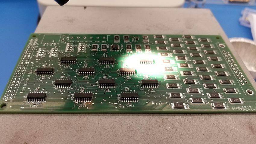
The completed control circuit is one component in the control unit which is pictured in
full in Fig 3.4. The control unit consists of a power supply, Arduino, DAC, and the control
circuit and is installed in a 260 mm x 160 mm aluminum box. The unit’s power supply
(including ±15 V and 5 V sources) is connected to the control circuit with screw-clamped
terminals and the switching enables from the Arduino, the I2 C data from the Arduino, and
the current-sense analog output to the Arduino are connected with female header sockets.
The power and digital control for the DAC is passed from the control circuit to the DAC
through a nodeLynk I2 C connector. The DAC analog output returns to the control circuit
at the screw-clamped terminal block. The control circuit outputs are bused over a ribbon
cable to a female DSUB connector that can be connected to a DSUB cable on the outside of
the box. The ribbon cable came with a female DSUB socket at one end and we connected
another female connector at the other end by soldering and then heat-shrinking each of the
25 leads. The control unit is powered by 120 V alternating current from a wall outlet and is
20CHAPTER 3. PMM UNIT DESIGN
Figure 3.3: The surface-mounted components of the PMM control circuit are installed using
a reflow soldering process. Using a microscope, solder paste is applied to each pad and
components are placed on the solder paste. The board is then heated on a hot plate until
the solder paste re-flows and the components are soldered. The surface-mounted components
installed in this process are the capacitors, resistors, switches, opamps, and the current-sense
IC.
Figure 3.4: The PMM control unit with all components installed. The control circuit (1)
is connected to the Arduino (2) over male-male header wires. The connections between the
control circuit and the Arduino include the switch enables, the I2 C data connections, and the
current-sense analog output. The control circuit passes the I2 C data along to the DAC (3)
which generates an analog voltage that returns to the control circuit. The board is powered
by a ±15 V and 5 V power supply (4). All components are secured to the aluminum box
using standoffs. The Arduino is controlled over USB (5) and the control circuit outputs are
delivered to a DSUB connector (6).
21CHAPTER 3. PMM UNIT DESIGN
controlled over a USB connection to the Arduino.
3.4 Control Software
The control unit can be addressed using the USB connection to the Arduino, which in turn
has control over the switches and the DAC and can measure the output of the current-sense
circuit. The software loaded on the Arduino is simple and serves the primary purpose of
acting as a translator for basic instructions that we deliver over the USB interface. All
control logic, routines, and algorithms are coded in a PMM control software suite in Python
which sends simple commands for enabling switches, setting the DAC input, and reading
analog voltages over a serial connection with the Arduino. Using this software configuration,
the control unit can be controlled in real-time through an iPython terminal session.
Functionality of the Python software suite includes basic features such as automation
for setting reverse currents, locks to prevent short circuits or current-overload on the board,
and routines for calibrating the control unit’s voltage/current setting abilities. The software
suite also includes algorithms for automatically correcting resonator frequency placement and
automatically mapping resonators in frequency space to their coordinates on the array. These
features require feedback from a resonator array and are discussed in detail in Chapter 5.
In addition to setting magnetization with a constant current applied to an intersection,
the board also needs to be able to reset the magnetization at each row/column intersection.
Because ferromagnets exhibit hysteresis, resetting their magnetization must be performed
by following the hysteresis curve and requires magnetic field (and therefore current) to vary
as a function of time (example scope trace pictured in Fig 4.7). The software suite includes
functionality for setting arbitrary time dependent voltages on the DAC. Because the serial
interface between the Arduino is not clocked and is slow, it is impossible to deliver the
instructions for a fast, time-varying voltage in real-time. Instead, the feature is implemented
by digitizing the signal in Python, and sending a time series of digitized voltages as well
as the intended time resolution to the Arduino. Custom code is implemented on-board the
Arduino to receive this data, store it in memory, and “replay” it through the DAC.
22Chapter 4
PMM Unit Characterization
After assembling the control unit and programming some simple control algorithms, we
tested and characterized the control circuit’s outputs. Characterization is an important
step to make sure that the control unit works properly and that it meets the intended
specifications before using it with a real MKID array.
4.1 Voltage Setting
Row and column currents in the circuit are specified by using a the 16-bit digital to analog
converter (DAC) as a voltage source. The digital input of the DAC is controlled by the
Arduino and its voltage range is between 0 V and Vcc (≈ 5 V). To maximize the precision
of this voltage setting, we calibrate it with respect to the internal reference voltage of the
Arduino.
Calibration is performed by sending a range of binary values to the DAC and measuring
the resulting voltages with reference to the internal diode of the Arduino. The results of this
measurement are shown in Fig 4.1. In this figure, the measured voltage remains unchanged
across multiple requested voltages because we can set voltages with 16-bit precision but
the Arduino is only capable of 12-bit measurement. To create a calibration function, we
generated a curve that intersects the mean of each step. We enforced that the curve is not
averaged on the first step, and that it instead intersects (0, 0).
Slightly better accuracy can be achieved when the interpolation is not smoothed and
23CHAPTER 4. PMM UNIT CHARACTERIZATION
Figure 4.1: Measured voltage (12-bit precision) versus requested voltage (16-bit precision) as
set by the DAC and measured by the Arduino. The calibration curve is defined by starting
at (0,0) and passing through the average requested voltage for each measured voltage.
instead follows the measurements point-by-point. However, this comes at the sacrifice of
limiting our setting resolution by the resolution of our Arduino measurements, the former
being 16 bits and the latter being only 12. The continuous interpolation also allows us to
sweep voltages at higher resolution with the DAC without lower resolution (≈ 5 mV) steps.
Figure 4.2 shows the percent error in voltage before and after calibration.
4.2 Current Measurement
To judge whether we are setting currents properly, we measure total current through all rows
and columns using the integrated INA213 current-sense circuit. This circuit is characterized
by it’s bias and gain.
4.2.1 Voltage Bias
The output of the INA213 is biased by ≈ 21 Vcc using a voltage divider. However, the bias is
not precisely 12 Vcc because of slight differences between the resistors in the voltage divider.
A more accurate value is found by taking a long (10 second) average of the true bias with
the DAC off and comparing this to the expected bias of 12 Vcc. We record the difference
24CHAPTER 4. PMM UNIT CHARACTERIZATION
(a) Test 1 (b) Test 2
Figure 4.2: Comparison of DAC error without (left) and with (right) calibration. Error is
reported as percent error.
(labeled ∆V0 ) each time the board is powered on in order to account for discrepancies in Vcc
from the power supply. We use 21 Vcc + ∆V0 as our bias when using the INA213 to measure
currents. Typical values of this discrepancies are measured to be ∆V0 = 7.4 mV ± 0.7 mV.
4.2.2 Gain
The gain measurement of the INA213 can be characterized with using two values: internal
gain (specified to be G ≈ 50) and sense resistance. It is challenging to try to distinguish
the individual contributions, so we instead take the equivalent approach of assuming G = 50
and accounting for all sources of gain error in the sense resistor measurement.
To determine the resistance of the sense resistor, we use a digital multi-meter to measure
the voltage across the resistor as a function of current which we control with the DAC. This
data is plotted in Fig 4.3 which shows the resistance measured by fitting the slope of this line.
The current across the resistor was set using the DAC and measured using the multi-meter
in current measurement mode, then the multi-meter was switched to voltage measurement
mode to measure the differential voltage. The nominal value for the sense resistor is specified
as 100 mΩ ± 1 mΩ. Our measurement of the resistance from the voltage supply to ground
yields a value of 115 mΩ ± 3 mΩ. This value is expected to be higher than the nominal
value because the trace and solder contribute additional resistance.
25CHAPTER 4. PMM UNIT CHARACTERIZATION
Figure 4.3: Sense resistance is measured by fitting multimeter data.
4.3 Current Setting
The purpose of our instrument is to set precise currents across selected intersections of
rows and columns. We have calibrated our voltage source and current measurement now
characterize our ability to set currents.
4.3.1 Linearity with Voltage
We use the INA213 current-sense circuit to measure total current through the board. The
INA213 outputs a voltage that is proportional to measured current and this voltage is read
by the Arduino’s built in ADC. This ADC has only 12 bits precision which corresponds to
a vopltage resolution of 4.9 mV. Accounting for the gain of the INA213 output voltage, this
corresponds to a current measurement resolution of 0.85 mA. We aim to set currents through
the board on the order of milliamps, so this measurement resolution is not ideal for testing
and calibration.
Figure 4.4a shows currents measured using the INA213 over a sweep of ninety voltages
which were set with only one row switched open. The digitization of the measurements by
the Arduino’s ADC are clearly visible but we can still tell that the current is nicely linear
with voltage.
26CHAPTER 4. PMM UNIT CHARACTERIZATION
(a) Single Channel (b) All Channel
Figure 4.4: Current measurements over a sweep over voltages for a single channel (a) and all
channels (b). For small currents, digitization in measurement by the Arduino’s 12 bit ADC
is visible. Linearity begins to break down for large currents starting at approximately 250
mA.
We also sweep voltages with multiple channels enabled to ensure that sourcing higher
currents does not damage our current linearity. Figure 4.4b shows the current linearity will
all rows and columns enabled. The linearity barely starts to break at the end of the range,
which may be due to nonlinearities in the opamp voltage amplification.
4.3.2 Accuracy
Current setting accuracy is hard to measure because of limitations in our ADC resolution.
As stated above, we have 0.85mA between ADC steps. This corresponds to fractional error
of up to 8.5% at currents of 10 mA due to limitations in measurement alone. Error for a
sample of set currents is plotted in Fig 4.5. The vertical lines mark the gap in which current-
setting was not measured. In this region, error can shoot up to close to 70% because of the
issue with the Arduino ADC resolution being so rough compared to such small set-currents.
4.3.3 Max Currents
By measuring where the amplified voltage diverges from its linear behavior, we set a cap on
our allowed voltage outputs from the DAC. For this board we set a generous cap of 3.5 V.
We measure multi channel current maximums by setting the voltages of each intersection to
3.5 V one-by-one, and measuring the total current through the board. A histogram of the
27CHAPTER 4. PMM UNIT CHARACTERIZATION
Figure 4.5: Fractional error in current setting according to measurements by the 12 bit ADC
on-board the Arduino. There is an inherent measurement error caused by the resolution of
the ADC.
positive and negative max currents for each intersection is plotted in Fig 4.6.
There are two outliers which are unlikely to be faulty resistors because they appear
only for positive max voltages. The source of these outliers still needs to be investigated.
Regaurdless of the shape of this distribution or its outliers, we conclude that we can be
confident in our ability to get at least 30 mA of positive of negative current across any one
intersection.
4.4 Row and Column Resistors
The row and column resistors can be measured autonomously using a function that sets the
voltage on each row and column individually and reads the current using the INA213. In
total there are 38 resistors: one “primary” and one “auxiliary” for each row column, with
there being 9 rows and 10 columns on the current version of the board.
The “primary” resistors are designed to let current into the intersection of interest and
are rated at 620Ω with ±1% variance, while “auxiliary” resistors are designed to limit the
counteracting current into all other intersection and are rated at 2400Ω with ±1% variance.
Table 4.1 shows the resistor values as measured using the INA213 current sense circuit.
28CHAPTER 4. PMM UNIT CHARACTERIZATION
Figure 4.6: Histogram of maximum currents for each intersection when set to a voltage of
±3.5 V. All intersections are able to achieve a current of greater than 30 mA.
1 2 3 4 5 6 7 8 9
Prim 641 640 640 643 637 637 638 642 637
Aux 2504 2516 2516 2510 2504 2517 2499 2517 2510
(a) Column Resistances [Ω].
1 2 3 4 5 6 7 8 9 10
Prim Unk. Unk. 645 644 644 644 645 642 650 641
Aux Unk. Unk. 2504 2492 2516 2504 2510 2517 2510 2517
(b) Row Resistances [Ω].
Table 4.1: Value of each primary and auxiliary resistor for each row and column as measured
by reading from the INA213 current-sense circuit. The measured average for the smaller
resistor is Rsmall = 641.86 Ω with 2σsmall = 6.60 Ω and the average for the larger resistor is
Rbig = 2509.57 Ω with 2σbig = 14.36 Ω.
29CHAPTER 4. PMM UNIT CHARACTERIZATION
Figure 4.7: Oscilloscope capture of time-dependent voltage for resetting hysteretic magne-
tization. The decaying sine traces the hysteresis curve for the magnetization back to zero
magnetization.
We predict a random error of approx 0.26% from digitization of ADC measurements,
and systematic error of 2% from factory precision plus up to 5.2% in the sense resistor value
using 2σ error. The systematic error corresponds to an actual resistance for our batch of
620 Ω resistors between 575 Ω and 665 Ω. For the 2400 Ω resistors, we would expect our
batch to have an actual resistance anywhere between 2230 Ω and 2570 Ω. Neither of these
ranges disagree with our measurements.
4.5 Reset Function
Setting the magnetization of a ferromagnet to zero requires a time dependent magnetic
field to follow the hysteresis curve through multiple cycles. An oscilloscope trace of the
proposed reset function is shown in Fig 4.7. This demonstrates the control unit’s ability to
set time-dependent voltage signals with high resolution. The specific reset function tested is
an exponentially decaying sine wave. The function is not smooth when crossing zero because
there is additional logic required to switch Vtop and Vbottom at this point. The exact delay
still needs to be investigated.
30Chapter 5
PMM Simulation
There are several functionalities of the PMM control software that operate using feedback
from a resonator array. These functionalities include automatic routines for correcting res-
onator frequency placements and for mapping resonator frequencies to their physical coor-
dinates in the array. For such routines, the control software needs to be able to measure
the frequency response of the MKID array and apply currents correspondingly. Using a real
MKID array while developing these routines inhibits other research in the lab because there
is only a limited number of cryogenic test beds. To work around this problem, we develop a
simulation module for the control software that allows us to simulate frequency readout of a
real MKID array. The simulation module is operated with the same current-setting software
that is used with the physical control circuit.
5.1 Modeling Hysteresis
The first step in designing the PMM simulation module was modeling the magnetization
of the ferromagnets in response to a current. We model the magnetic field through the
2
magnet as a function of current using B = µ0 R2 I/2(z 2 + R2 ) 3 , which is the expression for
the magnetic field on the axis of a current-carrying loop of wire. Here, R is the radius of the
current loop and z is its separation from the magnet along its axis.
The magnetization M of the ferromagnet in response to the applied field cannot sim-
ply be represented as a function M (B). Instead, the magnetization follows a hysteresis
31CHAPTER 5. PMM SIMULATION
Figure 5.1: Example hysteresis curve for magnetization as a function of applied field. The
magnetization depends on the history of the system. The arrows represent the flow of time.
curve which at any point depends not only on instantaneous applied field, but also on the
history of previous magnetization [4]. An example hysteresis curve is plotted in Fig 5.1
where the arrows represent the flow of time. It can be seen that M (B = 0, t = 0) = 0 while
M (B = 0, t = t0 ) = M0 .
The method we use to model hysteresis in the PMM control software is the Preisach
model of hysteresis [6]. This model works using a system of nonlinear relays that flip sign
depending on the direction of the change in magnetic field. The model can be realized using
a two dimensional array filled with some initial set of real numbers where magnetization is
proportional to the sum of all elements in the array. Increasing magnetic field is modeled by
increasing the values in the array row-by-row while decreasing magnetic field is modeled by
decreasing the values in the array column-by-column.
For instance, we can start with a 3x3 magnetization array filled with zeros at t0 , in-
crease the magnetic field by two units at t1 , then decrease it back to zero units at t2 .
0 0 0 0 0 0
This results in magnetizations of M (t0 ) = sum 0 0 0 = 0, M (t1 ) = sum 1 1 1 = 6, and
0 0 0 1 1 1
0 0 0
M (t2 ) = sum 1 0 0 = 2. Using this scheme we can apply and remove a magnetic field and
1 0 0
32CHAPTER 5. PMM SIMULATION
have the system retain a magnetization. This toy example demonstrates hysteretic behavior,
but doesn’t exhibit all of the features of ferromagnetic hysteresis. By adjusting the starting
configuration of the array and the amounts we add/subtract from the rows/columns we can
achieve more realistic hysteresis curves. The curve we looked at previously in Fig 5.1 is an
example of one that was generated using this model.
Parameterizing the behavior of curves generated using the Preisach model is difficult.
Currently, we have developed methods to generate hysteresis curves with a given saturation
field, saturation magnetization, and retentivity1 . More work needs to be done on in this
direction so that PMM simulations can most accurately recreate the behavior of the physical
magnets. The ability to simulate arrays with varying parameters will also help us optimize
the design specification of the magnet array.
5.2 Modeling Resonator Response
~ 0 (~r, M ) as a function of its magne-
Each ferromagnet produces some magnetic field in space B
tization. This is the field that remains even after all currents are removed and penetrates the
~ 0 (~r, M ) can be modeled
superconductor to shift the frequency of the resonator. The field B
as that resulting from a hollowed-out coin shape (refer to Fig 2.2b) with bulk magnetization
M . For preliminary modeling purposes, we approximate this field as being from a solid coin
shape with bulk magnetization M .
We also approximate the penetration field at the superconductor as B 0 0 (M ) =
~ 0 (~
B r0 , M ) · ẑ, given the magnet and resonator both lay parallel to the xy plane and r~0 is the
location of the resonator. In general, the field will not necessarily be constant in magnitude
or direction throughout the superconductor, and this needs to be investigated further. We
model the shift in frequency of a resonator as δf ∼ (B 0 0 )2 following from work presented in
Kwon et al. [5].
(i) (i)
Once we calculate resonant frequency fr = f0 + δf (i) of each resonator i, the next step
is to simulate a the frequency readout as we saw previously in Fig 2.1. Simulating this
1
Retentivity is the magnetization remaining when the applied magnetic field is reduced to zero from the
saturation point.
33CHAPTER 5. PMM SIMULATION
readout consists of generating a frequency response curve for each resonator in the array and
summing them together. The frequency response curve for each resonator depends on its
resonant frequency and quality factor and is given by
Qm /Qc
|S21 |(f ) = 1 −
f − fr
1 + 2iQ ·
fr
where Q ≡ (1/Qc + 1/Qi )−1 , fr is the resonant frequency including δf , and Qi and Qc
are respectively the internal and coupling quality factors. We simulate fabrication error by
applying random variance to the quality factors and resonant frequency of each resonator.
Finally, we in add high-frequency and low-frequency random noise to simulate measured
data.
5.3 Resonator Tuning
Simulating detector readout allows us to test algorithms for automatic frequency mapping
and overlap correction. The main process in frequency mapping is to image the array fre-
quency readout, then apply a shift to a resonator at a known coordinate and image the
readout again. A difference plot between the pre- and post-shift readout images can be ana-
lyzed using peak-detection and image processing to determine the resonant frequency of the
targeted resonator and whether it was originally overlapped. After all resonator frequencies
are mapped, corrections can be made simply by setting the magnetization at each resonator
with a temporary current.
34Conclusion
The ability to shift the resonant frequency of superconducting resonators in-situ would im-
prove pixel count of MKID arrays by enabling the correction of fabrication errors. Such
an improvement would reduce the cost of multi-thousand pixel MKID arrays and increase
the efficacy of MKIDs for high-resolution, high-sensitivity astronomical imaging. Increased
spatial resolution for kinetic inductance detector arrays would be beneficial for several areas
of research such as those that involve the direct observation of exoplanets.
Here we proposed a control circuit for multiplexing electrical currents through a grid of
electromagnets (the PMM array) that will be used to tune the resonant frequency of pixels
in a MKID array. The PMM array will correct overlapping resonators and identify swapped
resonators by shifting the resonant frequency of the MKIDs using an applied magnetic field.
The ability to make such adjustments post-fabrication allows for a closer spacing of resonant
frequencies in design. For this reason, we project that the PMM control circuit and array
will help improve the pixel yield of a MKID array by a factor of four or more. Improvements
to resonator spacing in frequency space will also help decrease the cost and complexity of
room-temperature readout electronics, both of which scale with frequency bandwidth.
The resonator frequency tuning algorithms that will be performed by the PMM control
circuit have thus far only been tested in simulation. A next step for this research will be to
test resonator tuning on a physical array. In addition, the prototype PMM control unit that
we describe in this work has the ability to multiplex currents over only 90 intersections. A
future direction will be to investigate modifications to the control unit that will allow it to
scale to arrays with several thousand pixels.
35Bibliography
[1] Pascal J. Borde and Wesley A. Traub. “High-Contrast Imaging from Space: Speckle
Nulling in a Low-Aberration Regime”. In: The Astrophysical Journal 638.1 (2006),
pp. 488–498. issn: 0004-637X. doi: 10.1086/498669. arXiv: 0510597 [astro-ph].
[2] D Flanigan et al. “Magnetic field dependence of the internal quality factor and noise
performance of lumped-element kinetic inductance detectors”. In: Applied Physics Let-
ters 109.14 (Oct. 2016), p. 143503. issn: 0003-6951. doi: 10.1063/1.4964119. url:
https://doi.org/10.1063/1.4964119.
[3] J E Healey et al. “Magnetic field tuning of coplanar waveguide resonators”. In: Applied
Physics Letters 93.4 (July 2008), p. 43513. issn: 0003-6951. doi: 10.1063/1.2959824.
url: https://doi.org/10.1063/1.2959824.
[4] D. C. Jiles and D. L. Atherton. “Theory of ferromagnetic hysteresis (invited)”. In:
Journal of Applied Physics 55.6 (1984), pp. 2115–2120. issn: 00218979. doi: 10.1063/
1.333582.
[5] Sangil Kwon et al. “Magnetic field dependent microwave losses in superconducting
niobium microstrip resonators”. In: Journal of Applied Physics 124.3 (July 2018),
p. 33903. issn: 0021-8979. doi: 10 . 1063 / 1 . 5027003. url: https : / / doi . org /
10.1063/1.5027003.
[6] I D Mayergoyz. Mathematical models of hysteresis and their applications. 1st ed.. Am-
sterdam: Amsterdam, 2003.
[7] B A Mazin et al. “ARCONS: A 2024 Pixel Optical through Near-IR Cryogenic Imaging
Spectrophotometer”. In: Publications of the Astronomical Society of the Pacific 125
36BIBLIOGRAPHY
(Nov. 2013), p. 1348. issn: 0004-6280. doi: 10 . 1086 / 674013. url: https : / / ui .
adsabs.harvard.edu/abs/2013PASP..125.1348M.
[8] Benjamin A Mazin et al. “A superconducting focal plane array for ultraviolet, optical,
and near-infrared astrophysics”. In: Optics Express 20 (Jan. 2012), p. 1503. issn: 1094-
4087. doi: 10.1364/OE.20.001503. url: https://ui.adsabs.harvard.edu/abs/
2012OExpr..20.1503M.
[9] Seth R. Meeker et al. “DARKNESS: A Microwave Kinetic Inductance Detector Integral
Field Spectrograph for High-contrast Astronomy”. In: Publications of the Astronomical
Society of the Pacific 130.988 (2018), p. 065001. doi: 10.1088/1538-3873/aab5e7.
[10] Bernard J. Rauscher et al. “Detectors and cooling technology for direct spectroscopic
biosignature characterization”. In: Journal of Astronomical Telescopes, Instruments,
and Systems 2.4 (2016), p. 041212. doi: 10.1117/1.JATIS.2.4.041212.
[11] Pieter J. de Visser et al. Phonon-trapping enhanced energy resolution in superconduct-
ing single photon detectors. 2021. arXiv: 2103.06723 [astro-ph.IM].
[12] Alexander B. Walter et al. “The MKID Exoplanet Camera for Subaru SCExAO”. In:
Publications of the Astronomical Society of the Pacific 132.1018 (2020), p. 125005. doi:
10.1088/1538-3873/abc60f.
[13] Rogier A. Windhorst et al. “Generation-X: An X-ray observatory designed to observe
first light objects”. In: New Astronomy Reviews 50.1-3 (2006), pp. 121–126. doi: 10.
1016/j.newar.2005.11.019.
[14] Nicholas Zobrist et al. “Wide-band parametric amplifier readout and resolution of op-
tical microwave kinetic inductance detectors”. In: Applied Physics Letters 115.4 (July
2019), p. 042601. doi: 10.1063/1.5098469.
37Appendix A
Improving Energy Resolution
38Improving energy resolution in photon counting Microwave Kinetic
Inductance Detectors using principal component analysis
Jacob M. Millera , Nicholas Zobrista , Benjamin A. Mazina
a
University of California, Department of Physics, Santa Barbara, CA, USA, 93106
Abstract. We develop a pulse processing method for Microwave Kinetic Inductance Detectors (MKIDs) that is based
on principal component analysis (PCA). PCA can be used to characterize the variation in a photon pulse and therefore
does not rely on the energy-independent pulse shape assumption made in standard filtering techniques. As such, a
PCA-based energy measurement is especially useful for applications where the detector response is near its saturation
point. It has been shown previously that PCA using two principal components can be used as an energy-measurement
scheme. We extend upon these ideas and develop a method for measuring the energies of photon pulses by characteriz-
ing the pulse shape with an arbitrary number of principal components and an arbitrary number of calibration energies.
This technique improves a previously-reported TKID (Thermal KID) energy resolution from 75 eV to 43 eV at 5.9
keV. We also demonstrate this technique on data from an optical to near-IR MKID and achieve energy resolutions that
are consistent with the best results from existing analysis techniques.
1 Introduction
Microwave Kinetic Inductance Detectors (MKIDs) are superconducting sensors1, 2 used for sensi-
tive astronomical observations. These devices use changes in the surface impedance of a supercon-
ductor to sense individual photon impacts with up to microsecond precision. The superconductor
is patterned into a microwave resonator which allows each sensor to be addressed at a different fre-
quency on the same feedline. This multiplexing scheme dramatically simplifies the readout of the
system compared to other superconducting detector technologies, and large arrays of up to 20,000
detectors have already been demonstrated.3, 4
An important quality in an MKID is the precision with which it can measure the energy of
each incident photon — its energy resolution. For MKIDs operating in the optical wavelength
range, improvements to the energy resolution open the way for accurate spectral measurements of
planets orbiting other stars.5 In the X-ray regime, thermal KIDs (TKIDs) have been proposed as an
alternative to the more sensitive but harder to multiplex transition edge sensors (TESs). Closing the
A-1You can also read