OLED - Status quo and our position - Information Day 2013 - A Deep Dive into the LC&OLED Business - EMD Group
←
→
Page content transcription
If your browser does not render page correctly, please read the page content below
OLED – Status quo and our position
Information Day 2013 – A Deep Dive into the LC&OLED Business

Dr. Udo Heider
Vice President OLED

Darmstadt, Germany – June 26, 2013
Disclaimer

Remarks
All comparative figures relate to the corresponding last year’s period.

Important information
This presentation does not constitute an offer of securities for sale or a solicitation of an offer to purchase securities in the
United States. The shares referred to herein have not been and will not be registered under the U.S. Securities Act of 1933,
as amended (the “Securities Act”), and may not be offered or sold in the United States absent registration under the
Securities Act or an available exemption from such registration.

Note regarding forward-looking statements
The information in this document may contain “forward-looking statements”. Forward-looking statements may be identified
by words such as “expects”, “anticipates”, “intends”, “plans”, “believes”, “seeks”, “estimates”, “will” or words of similar
meaning and include, but are not limited to, statements about the expected future business of Merck KGaA, Darmstadt,
Germany resulting from the proposed transaction. These statements are based on the current expectations of management
of Merck KGaA, Darmstadt, Germany and E. Merck KG, Darmstadt, Germany and are inherently subject to uncertainties
and changes in circumstances. Among the factors that could cause actual results to differ materially from those described in
the forward-looking statements are factors relating to satisfaction of the conditions to the proposed transaction, and changes
in global, political, economic, business, competitive, market and regulatory forces. Merck KGaA, Darmstadt, Germany and
E. Merck KG, Darmstadt, Germany do not undertake any obligation to update the content of this presentation and forward-
looking statements to reflect actual results, or any change in events, conditions, assumptions or other factors.
All trademarks mentioned in the presentation are legally protected.
Agenda

OLED at Merck KGaA, Darmstadt, Germany and basics

OLED vapor versus printing

Our perspective on OLED

Strategic update and position

Summary

We start from strong platforms

                                          The Group’s position in display materials

        Commercial platform                                                                Technology platform
         in display materials                          OLED activities                     in display materials

    No. 1 in liquid crystals with >60%               Strong IP position with          ~500 people in R&D with a powerful
               market share                           high research output                   budget of > €100 m

                                                    Broad R&D cooperation
                                                                                         Broad R&D approach across
          Innovation leader in                     with academia and industry                display value chain:
            display materials
                                                                                          LC, RM, phosphors, OLED
                                                   Systematic R&D for OLED
                                                     in vapor and printing
     Highly flexible and cost-leading
                                                                                          State-of-the-art know-how
                operations

                                                                                            Research centers and
  Established and strong collaborations
                                                                                       development hubs in key regions,
          with all display makers
                                                                                              close to customers

                                                                                                                           5
OLED: A fundamental part of our R&D strategy for
more than a decade
Our history of OLED development
OLED activities in Mainz
2001 OLED today
Schott & IBM Project Luminescence Technologies
We acquired Project Luminescence Technologies
~80 R&D experts
First white OLED lighting designs for ambient lighting
New strategy from component manufacturer to material
2007 supplier 2010 M&S experts in all
4 key countries
Merging of both
OLED activities in Frankfurt
in Darmstadt
1992
Hoechst AG R&D Project ~1,400 patents
Covion GmbH established
100% subsidiary of Avecia Ltd. Commercial
100% subsidiary of Merck KGaA, Darmstadt, Germany production
Integration into Merck KGaA, Darmstadt, Germany
2007
6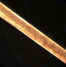
OLEDs are carbon-based light-emitting components

                           Fundamentals of liquid crystals versus OLED                              Advantages of OLED

   Liquid crystals - Light Modulation                    OLED - Light Generation
                                                                                                    OLED displays versus
                                                                                                    liquid crystal displays

                                                                                                        Slightly thinner

                                                                                                        Slightly lighter
   Electrodes

                                                                             Electrodes
                                                                                          3–6V
                                                           OLED
                               Light Source
                                                                                                 OLED: A fully controllable
                Light Source                                                                      micro light bulb with the
                                                                                                 correct color in every pixel

                                                                                                                                7
Our focus is to provide solutions for the full OLED
stack, addressing all layers
                                       Setup of a typical OLED stack

                                                                       Cathode                 Metal
                                                                        100-200nm

                                    ------
                                                                         EIL             Electron Injection
                                                                          20nm

    Human hair
                                              +                         ETL
                                                                          20 nm          Electron transport
                                                                        HBL
                                    -- -

                                                                                                                 Our target
                                                                          10nm

                  ~400x                                                                    Hole Blocking
                 thinner    3-6 V        -+                             EML
                                                                         20-40nm

                                         +
                                                                                     Emission Red, Green, Blue
                                                                                      (Matrix 95% +Emitter5%)
                                        +                                HTL
                                                                          20nm

                                        +                                                 Hole Transport

                                                                         HIL
                                    ++++++                                5-150 nm
                                                                                           Hole injection

                                                                   Transparent
                                                                      Anode               Indium tin oxide

                           Interaction of layers determine OLED performance

                                                                                                                              8
OLED can be used for display as well as lighting
applications
Our OLED application fields
Flexible displays Lighting
Curved surfaces OLED lighting concepts
Non-breakable Wallpaper
Non-flexible displays Transparent
Very thin New applications
Low energy Combining displays
consumption and lighting
OLED is more than just TVs
9While further production capacities for OLED will be
built, their overall level will remain low near-term
Display surface area Announced OLED production capacities for displays Display production capacities
[km²]
by surface area in 2015
12
Taiwan
10
8 South Korea LCD, Plasma,
Samsung Display
CRT > 95%
6
OLED < 5%
South Korea
4 LG Display
2 Japan
0 China
2013 2015
OLED is more than just TVs
Source: DisplaySearch Quarterly FPD Supply/Demand & Capital Spending Report, Q1 2013, AMOLED, year-end capacities with likelihood >=30%
10Agenda OLED at Merck KGaA, Darmstadt, Germany and basics OLED vapor versus printing Our perspective on OLED Strategic update and position Summary
The development of OLED displays already started
20 years ago, gaining momentum only recently
                             Small display segment                Premium TV segment (> 47”)           Consumer TV segment (> 37”)

    Vapor                   11’’ TV
                                                   Smartphones
                                       15’’ TV                         55’’            > 47’’                      > 37’’

   Printing

    Producer

                     2000       2007             2010      2012     2013      2014              2015   >2015

          passive matrix                                                      active matrix

 OLED – from premium products to general consumer market as technology and process hurdles are overcome

                                                                                                                                     12
Today, two technologies are used for the commercial
production of OLED displays: RGB and White
Today's commercial manufacturing processes for OLED
Technology type
Production process RGB
Display and lighting
Small molecules RGB
Vapor
OLED
deposition White
Small molecules
white with color filter
While white OLED is easier to manufacture today, RGB OLED is likely to offer higher energy efficiency
Acronyms: RGB = Red, green and blue
13The vapor process for RGB OLED production has a
limited intrinsic yield
Chemical vapor deposition (CVD) process
Step 1: Application of red emission layer
Vacuum
Red OLED box
source Deposition yield:
OLED waste Fine metal
shadow maskThe vapor process for RGB OLED production has a
limited intrinsic yield
Chemical vapor deposition (CVD) process
Step 2: Application of green emission layer
Vacuum
Green OLED box
source Deposition yield:
OLED waste Fine metal
shadow maskThe vapor process for RGB OLED production has a
limited intrinsic yield
Chemical vapor deposition (CVD) process
Step 3: Application of blue emission layer
Vacuum
Blue OLED box
source Deposition yield:
OLED waste Fine metal
shadow maskRGB OLED vapor process is attractive for small
displays but is challenging for large displays
Characteristics of Chemical Vapor Deposition (CVD) process for RGB OLED
Pros Cons
Limited substrate size due to challenges
Established and well controllable process
arising from handling of large metal masks
High amount of waste due to need for
High resolution possible
masking
Successful in small devices Limited scalability
Uneven deposition of material
RGB OLED production based on chemical vapor deposition can hardly be cost competitive to LCD
17Printing is a proven technology for the targeted
deposition of materials
Technology of printing
Printer
head
OLED - Ink
Polymer
bank
TFT ITO Substrate
Due to targeted deposition, little waste is created in the printing process
Acronyms: TFT = Thin-film transistor; ITO = Indium tin oxide
18OLED printing: A scalable and efficient production
technology for displays, but still in its infancy
Characteristics of printing process
Pros Cons
Very efficient use of materials No established process
with high throughput for mass production yet
Requires availability of technology and
Scalability to large areas
corresponding inks
Less complex process
Open technology access
RGB OLED production based on printing has the chance to be cost competitive to LCD
19OLED printing can solve the waste dilemma and the
size limit of the RGB vapor process
Characteristics of OLED production technologies
Chemical vapor deposition OLED material waste Printing
>70%
?
2012 price per square inch: 2014 price per square inch:
~$10 US* ~$5 US*
No targeted deposition of Targeted deposition of OLEDAgenda OLED at Merck KGaA, Darmstadt, Germany and basics OLED vapor versus printing Our perspective on OLED Strategic update and position Summary
If OLED technology advances further, it could gain
meaningful share in the TV market
Market forecast for OLED surface area OLED market
Surface area Today, small displays play
[km²] OLED lighting
dominant role for OLED
Mobile PC/Phone OLED
OLED TV
Additional growth driver for OLED
60
could be TVs
OLED lighting is expected to play a
40 meaningful role from 2020 onwards
~10-15% of
20 total display
market
OLED could capture ~10-15%
of the total display market by 2019
0
2013 2016 2019
Source: DisplaySearch, Quarterly Worldwide Flat Panel Forecast Report, Q1 2013; Nanomarkets, Special Report for: The FlexTech Alliance - OLED Lighting Markets, May 2012
22RGB printing has technological advantages
compared to rivaling RGB vapor process
Comparison of OLED printing versus OLED vapor deposition
Processing
Printing Vapor deposition
Performance
Scale to large area
Materials
Advantage Less complex process Established state-of-the-art
High material utilization Suitable for ultra high
High production yield resolution
High throughput
Open technology access
Performance
Materials Scale to large area
No established production
Challenge Production yield
technology for OLED yet
Complexity of process
23Due to its scalability, OLED printing has the potential
to enter the large display mass market
Small displays Medium and large displays (TVs) Mass market (display surface)
High costs per square inch
compensated by high prices
for devices
Vapor
Challenging production yields today create significant
barriers to enter the mass market
If technological hurdles are overcome, an attractive “mass market“
Printing
cost-per-inch² ratio could serve the whole display market ready
Time
24Alliance of our company and EPSON creates
significant momentum in development of OLED printing
The Group’s commercialization roadmap of OLED printing Positioned for OLED printing leadership
Our position in OLED printing
Development
process Current status: Consolidated market
First OLED TV prototypes made We are one out of ~3 players
Q1 2010: Testing commercial production
Joint development
with EPSON
Our position in OLED vapor
Q2 2009: Fragmented market
Project start
We are among ~10 players
Cooperation with EPSON/TEL
Step change in OLED printing technology
Combined expertise creates highway to OLED
printing
We have positioned ourselves to
Time
become market leader in OLED
2009 2010 2011 2012 2013 2014 2015
printing
Combining our strong expertise in display materials with Epson’s strength in printing
25Agenda OLED at Merck KGaA, Darmstadt, Germany and basics OLED vapor versus printing Our perspective on OLED Strategic update and position Summary
OLED takes the same strategic approach that has
proven successful for liquid crystals
Value-adding strategy in liquid crystals and OLED
Single material supplier Solution provider
Limited development scope Difficult to exchange
Highly depending on “customer pull” Differentiation by performance
Can stimulate “customer push”
Accelerates technology development
triple win for customer, consumer and provider
Liquid Crystal Liquid crystal Translate chemistry into Customized liquid crystal
Strategy single material physics solution
OLED Customized OLED
OLED material Added value
Strategy full stack
27Transition to solution provider maximizes value
for us and our customers
Transitioning from supplying materials to providing solutions
Value
potential Full stack strategy
Strategy rationale
Address all layers and combinations
Be ready to move if market comes Understand the overall device
Careful spending according to Optimize the combination of materials
market development
Strategy rationale
Increase technical success by focus
Address needs of customers directly
Common strategy Be a competent partner
Speed up development
Concentration of development on few Achieve sustainable technical position
layers with good IP base (beyond IP in singles)
Be ready for printable technology
Material supplier Solution provider
Time
28Agenda OLED at Merck KGaA, Darmstadt, Germany and basics OLED vapor versus printing Our perspective on OLED Strategic update and position Summary
If OLED takes off in large displays and lighting,
we are ready to participate

  Powerful commercial and technology platforms
  in display materials

  Strong position in OLED vapor and printing

  We are ready to capture the OLED opportunity

                                                    30
Appendix
White OLED displays: Higher yields in the vapor
process, but also higher energy consumption
                  Characteristics of Chemical Vapor Deposition (CVD) process for white OLED

                        Pros                                                      Cons

          Established and well-controllable process                           Highly complex stack

                  High resolution possible                               Uneven deposition of material

                                                                         ~2/3 of light intensity held back
                Successful in small devices
                                                                                   by color filters

                    No need for masking

    White OLED displays: easier to manufacture, but even less differentiation to LCD than RGB OLED

                                                                                                             33
You can also read


