AN12395 OM-SE050ARD hardware overview Rev. 1.1 - 27 June 2019 534311 - NXP Semiconductors
←
→
Page content transcription
If your browser does not render page correctly, please read the page content below
AN12395
  OM-SE050ARD hardware overview
  Rev. 1.1 — 27 June 2019                                                Application note
  534311

Document information
Information     Content
Keywords        OM-SE050ARD, SE050
Abstract        This document describes the OM-SE050ARD development kit and details
                how to use its jumpers to configure the different communication options with
                the SE050 security IC.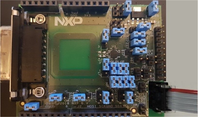
NXP Semiconductors
                                                                                                                                 AN12395
                                                                                                                   OM-SE050ARD hardware overview

Revision history
Revision history
Revision       Date         Description
number
1.0            2019-06-08   First document release.
1.1            2019-06-27   Corrected an error in Figure 2 pin description.

AN12395                               All information provided in this document is subject to legal disclaimers.                 © NXP B.V. 2019. All rights reserved.

Application note                                     Rev. 1.1 — 27 June 2019
                                                              534311                                                                                         2 / 24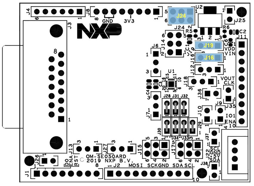
NXP Semiconductors
                                                                                                                                 AN12395
                                                                                                                   OM-SE050ARD hardware overview

1         Read this first
                       This section lists the hardware and software required before starting this document.

                   1.1 Required hardware
                       OM-SE050ARD development kit:

                       Table 1. OM-SE050ARD development kit details
                       Part number                   12NC                                          Content                    Picture
                       OM-SE050ARD                   935383282598                                  SE050 development
                                                                                                   board

                   1.2 Required software
                       This document does not use or install any specific software tool or package.

AN12395                               All information provided in this document is subject to legal disclaimers.                 © NXP B.V. 2019. All rights reserved.

Application note                                     Rev. 1.1 — 27 June 2019
                                                              534311                                                                                         3 / 24
NXP Semiconductors
                                                                                                                               AN12395
                                                                                                                 OM-SE050ARD hardware overview

2         Overview
                     The OM-SE050ARD is the development kit for the SE050 Plug & Trust product family.
                     This kit allows you to evaluate the SE050 product family features and simplifies
                     the development of your custom applications. Figure 1 shows a picture of the OM-
                     SE050ARD.

                     Figure 1. OM-SE050ARD development kit
                                         2
                     The SE050 uses I C as communication interface and its commands are wrapped using
                     the Smartcard T=1 over I²C (T=1oI2C) protocol. In addition, the SE050 supports the
                     following interfaces:
                       2
                     • I C interface in slave mode with date rates up to 3.4 Mbps .
                        2
                     • I C interface in master mode with date rates up to 400 Khz.
                     • ISO/IEC 14443 T=CL protocol.
                     The OM-SE050ARD flexible design makes it possible to access the SE050 interfaces by
                     just changing a few jumper settings.
                                     2                                                                            2
                     Note: Only the I C slave interface is mandatory. The I C master and ISO/IEC 14443
                     interfaces are optional.

AN12395                             All information provided in this document is subject to legal disclaimers.                 © NXP B.V. 2019. All rights reserved.

Application note                                   Rev. 1.1 — 27 June 2019
                                                            534311                                                                                         4 / 24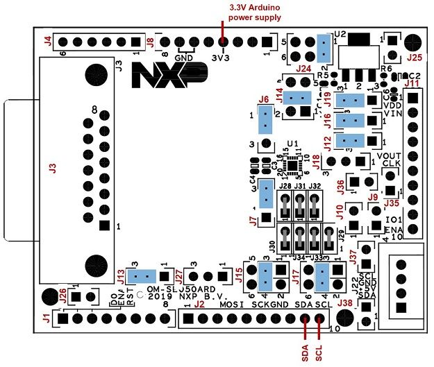
NXP Semiconductors
AN12395
OM-SE050ARD hardware overview
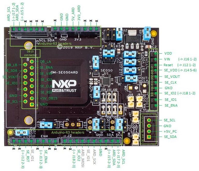
3 Headers and connectors
The OM-SE050ARD is designed with several headers and connectors that allow you to
interface with SE050. The OM-SE050ARD is equipped with:
• Arduino-R3 header: It allows you to easily attach it to any NXP MCU/MPU
development board with Arduino compatible headers such as many Kinetis, LPC and
i.MX MCU boards. The Arduino-R3 female connectors come soldered in the OM-
SE050ARD.
2
• External I C connector: It allows you to connect any non-Arduino compatible MCU
2
boards via I C slave interface. The OM-SE050ARD includes the mounting holes for the
2
External I C connector.
2
• 10-pin header: It allows you to access several pins of the SE050, including the I C
master interface to attach sensors or peripherals to the board. The 10-pin header male
connectors come soldered in the OM-SE050ARD.
• DB15 header: It allows you to access several pins of the SE050, including the ISO/IEC
2
14443 or the I C master interface to attach sensors or peripherals to the board. The
OM-SE050ARD includes the mounting holes for the DB15 connector.
Figure 2 shows an overview to OM-SE050ARD headers and connectors together with its
corresponding pin description.
Figure 2. OM-SE050ARD headers and connectors overview
AN12395 All information provided in this document is subject to legal disclaimers. © NXP B.V. 2019. All rights reserved.
Application note Rev. 1.1 — 27 June 2019
534311 5 / 24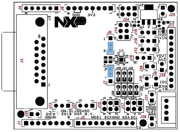
NXP Semiconductors
                                                                                                                                       AN12395
                                                                                                                    OM-SE050ARD hardware overview

4         Jumpers overview
                       The OM-SE050ARD board uses individual jumpers to configure settings related with the
                       SE050 interfaces, power supply and power modes. This section provides an overview to
                       the OM-SE050ARD jumpers and its configuration options.

                        2
                   4.1 I C configuration
                                                                                                                                                              2
                       The OM-SE050ARD has jumpers that allow you to control the configuration of the I C
                       slave and master interfaces available in SE050. These jumpers are:
                                                             2
                       • J9, J10: Configures the I C master pull up connection.
                                                   2
                       • J15, J17: Configures the I C slave connection.
                                                   2
                       • J37, J38: Configures the I C slave interface pull up resistor.
                                                                                                                               2
                       Table 2 describes the OM-SE050ARDjumper settings for each I C setting configuration.
                                                   2
                       Table 2. Jumpers for I C configuration
                       Jumper     Description                                    Open                               1-2                  3-4
                                  2
                       J9         I C Master pull up                             not connected                      3k3 Ohm              n.a.
                                  connection                                     (Default)
                                  2
                       J10        I C Master pull up                             not connected                      3k3 Ohm              n.a.
                                  connection                                     (Default)
                                  2
                       J15        I C Slave SDA connection not connected                                            Arduino R3 J4:5      Arduino R3 J2:9
                                                                                                                                         (Default)
                                  2
                       J17        I C Slave SCL connection                       not connected                      Arduino R3 J4:6      Arduino R3 J2:10
                                                                                                                                         (Default)
                       J18        SE050_IO2 routing                              n.a                                Routed to J11:9      Routed to J2:3
                                                                                                                    (Default)
                                  2
                       J37        I C Slave SCL pull up                          3k3 Ohm                            560 Ohm              n.a.
                                                                                 (Default)
                                  2
                       J38        I C Slave SDA pull up                          3k3 Ohm                            560 Ohm              n.a.
                                                                                 (Default)

                                                                                                                                   2
                       Figure 3 highlights in blue the location of theOM-SE050ARD for I C settings
                       configuration.

AN12395                                All information provided in this document is subject to legal disclaimers.                      © NXP B.V. 2019. All rights reserved.

Application note                                       Rev. 1.1 — 27 June 2019
                                                                534311                                                                                             6 / 24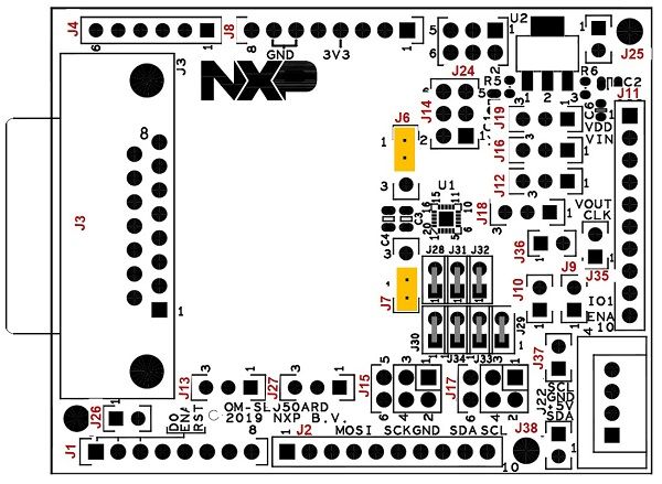
NXP Semiconductors
                                                                                                                                   AN12395
                                                                                                                   OM-SE050ARD hardware overview

                                                                                              2
                       Figure 3. OM-SE050ARD jumpers for I C settings configuration

                   4.2 Power supply options
                       The jumpers that allow you to change the OM-SE050ARD power supply settings are:
                       • J19: Configures VDD supply voltage options.
                       • J16: Connfigures SE050_VIN supply options.
                       • J24: Configures VDD supply voltage options in case the LDO is used.
                       Table 3 describes the OM-SE050ARDjumper settings for each power supply settings
                       configuration.

                       Table 3. Jumpers for power supply settings configuration
                       Jump    Description                        1-2                             2-3                   3-4               5-6
                       er

                       J16     SE050_Vin supply                   Supplied by                     Supplied by           n.a.              n.a.
                                                                  J11:2 pin                       the VDD (see
                                                                                                  J19)
                                                                                                  (Default)
                       J19     VDD supply voltage                 From LDO                        From 3V3_             n.a.              n.a.
                                                                                                  ARD pin
                                                                                                  (Default)

                       J24     VDD supply voltage                 From 5V_PC                      n.a.                  From 5V_          From 5V_ARD
                                                                             2
                               (if LDO is used)                   (External I C                                         DB15 pin          pin
                                                                  connector -
                                                                  Default)

                       Figure 4 shows the power supply unit schematics.

AN12395                               All information provided in this document is subject to legal disclaimers.                   © NXP B.V. 2019. All rights reserved.

Application note                                     Rev. 1.1 — 27 June 2019
                                                              534311                                                                                           7 / 24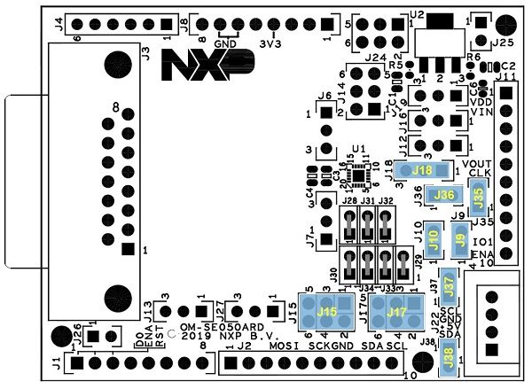
NXP Semiconductors
                                                                                                                             AN12395
                                                                                                               OM-SE050ARD hardware overview

                   Figure 4. OM-SE050ARD power supply settings

                   Figure 5 highlights in blue the location of theOM-SE050ARD for power supply settings
                   configuration.

                   Figure 5. OM-SE050ARD jumpers for power settings configuration

AN12395                           All information provided in this document is subject to legal disclaimers.                 © NXP B.V. 2019. All rights reserved.

Application note                                 Rev. 1.1 — 27 June 2019
                                                          534311                                                                                         8 / 24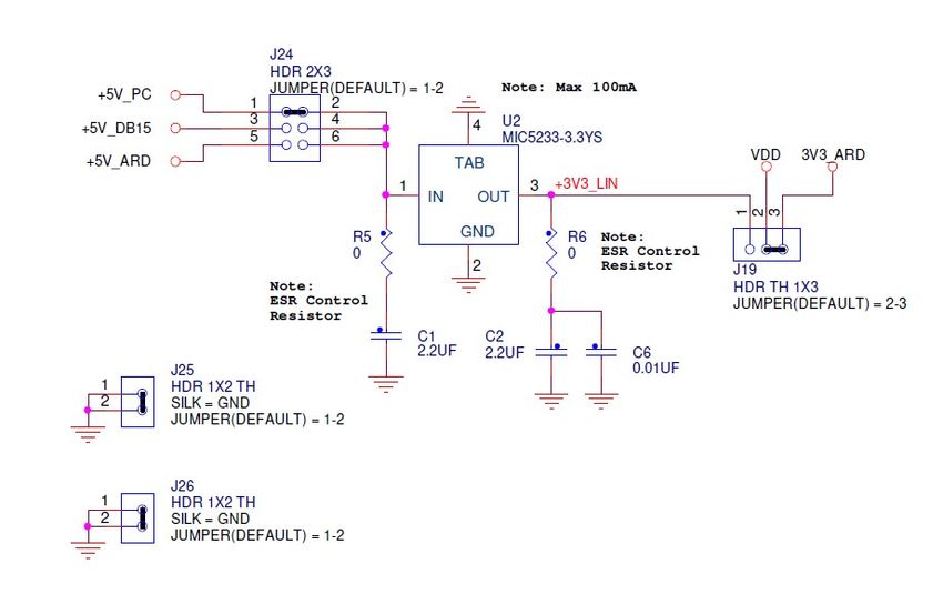
NXP Semiconductors
                                                                                                                                   AN12395
                                                                                                                   OM-SE050ARD hardware overview

                   4.3 Deep power-down mode
                      The deep power-down mode reduces the SE050 power consumption to the minimum. In
                                       2
                      this mode, only I C pads stay supplied via Vin. The deep power-down mode is enabled by
                      setting the ENA pin to a logic zero. In addition, it is required to supply Vin pin and connect
                      Vout and Vcc pins at the PCB level.
                      The ENA pin controls an internal switch between Vout and Vin as shown in Figure 6.
                      Therefore, if Vout is connected to Vcc, the ENA pin can effectively switch the power on
                      and off to Vcc.

                       Figure 6. Deep power-down mode diagram

                      The jumpers J13 and J14 of the OM-SE050ARD allow you to control the SE050 deep
                      power-down mode. To enable the deep power-down mode using the OM-SE050ARD:
                      • J13: Must be set to position 2-3.
                      • J14: Must be set to position 3-4.
                      Table 4 describes the OM-SE050ARD jumper settings for the deep power-down mode
                      configuration

                      Table 4. Jumpers for deep power-down mode configuration
                       Jumper Description                1-2                             2-3                           3-4                5-6

                       J13      SE050_ENA                ENA low.        ENA controlled                                n.a.               n.a.
                                pin routing              Switch disabled by Arduino R3
                                                                         (Default)

                       J14      SE050_VCC pin Routed to VDD                              n.a.                          Routed to          Routed to
                                routing       supply voltage                                                           SE050_Vout pin     J11:4 pin
                                                                                                                       (Default)

                      Figure 7 highlights in blue the location of jumper J13 and J14.

AN12395                               All information provided in this document is subject to legal disclaimers.                   © NXP B.V. 2019. All rights reserved.

Application note                                     Rev. 1.1 — 27 June 2019
                                                              534311                                                                                           9 / 24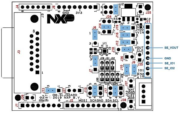
NXP Semiconductors
                                                                                                                                      AN12395
                                                                                                                    OM-SE050ARD hardware overview

                        Figure 7. OM-SE050ARD jumper J13 and J14 location

                   4.4 Reset pin routing
                                                                                     2
                       Jumper J12 allows you to control the I C reset pin routing of the SE050. Table 5 indicates
                       the J12 configuration.
                                                                                                               2
                       Note: The SE050 reset pin does not apply for the I C interface.

                       Table 5. Jumpers for reset pin routing configuration
                       Jumper     Description                                         Open                               1-2                        2-3
                       J12        SE050_RST pin                                       Not connected                      Routed to J11:3            Routed to
                                                                                                                         strip pin connector        Arduino R3
                                                                                                                                                    (Default)

                       Figure 8 highlights in blue the location of Jumper J12.

AN12395                                All information provided in this document is subject to legal disclaimers.                     © NXP B.V. 2019. All rights reserved.

Application note                                      Rev. 1.1 — 27 June 2019
                                                               534311                                                                                           10 / 24
NXP Semiconductors
AN12395
OM-SE050ARD hardware overview
Figure 8. OM-SE050ARD Jumper J12 location
4.5 ISO/IEC14443 contactless interface
Jumper J6 and J7 allow you to control the SE050 contactless interface and allows you to
select which antenna shall be used for contactless communication. Table 6 indicates J6
and J7 jumper settings.
Table 6. Jumpers for ISO/IEC14443 contactless interface settings
Jumper position Description
J6: 2-3 and J7: 1-2 Contactless operation disabled
J6: 1-2 and J7: 2-3 Contactless operation disabled (Default)
J6: 2-3 and J7: 2-3 Contactless operation enabled with OM-SE050ARD internal antenna
J6: 1-2 and J7: 1-2 Contactless operation enabled with external ID1 antenna through DB15
connector
Figure 9 highlights in blue the location of jumpers J6 and J7.
AN12395 All information provided in this document is subject to legal disclaimers. © NXP B.V. 2019. All rights reserved.
Application note Rev. 1.1 — 27 June 2019
534311 11 / 24NXP Semiconductors
AN12395
OM-SE050ARD hardware overview
Figure 9. OM-SE050ARD jumper J6 and J7 location
AN12395 All information provided in this document is subject to legal disclaimers. © NXP B.V. 2019. All rights reserved.
Application note Rev. 1.1 — 27 June 2019
534311 12 / 24NXP Semiconductors
AN12395
OM-SE050ARD hardware overview
5 OM-SE050ARD board use cases
This section details the jumper settings to configure the differnet interfaces and to enable
specific use cases with the OM-SE050ARD board.
5.1 SE050 via Arduino header
2
This section details the jumper configuration to enable the I C slave interface in the
2
Arduino header. The related jumpers of the OM-SE050ARD for I C slave interface
configuration are:
2
• J37 and J38: Configure the pull up resistors of the I C interface.
• J19: Configures VDD supply voltage options.
• J24: Configures VDD supply voltage options in case the LDO is used.
2
Table 7. Jumper settings for I C slave interface configuration
Jumper Configuration Comment
J6 Set to 1-2 Contactless operation disabled
(Default)
J7 Set to 2-3 Contactless operation disabled
(Default)
2
J9, J10 Set to I C master pull ups disabled
“Open” (Default)
J12 Set to 2-3 SE_RST routed to ARD_RST on J1:3
(Default)
J13 Set to 2-3 SE_ENA set to ARD_ENA on J1:6
(Default)
J14 Set to 3-4 SE_VOUT as SE_VDD
(Default)
2
J15 Set to 3-4 I C_SDA routed to ARD_SDA_R3 (J2:9)
(Default)
2
Set to 1-2 I C_SDA routed to ARD_SDA (J4:5)
J16 Set to 2-3 VDD as SE_VIN
2
J17 Set to 3-4 I C_SCL routed to ARD_SCL_R3 (J2:10)
(Default)
2
Set to 1-2 I C_SCL routed to ARD_SCL (J4:6)
J19 Set to 2-3 SE_VDD=3.3V from Arduino-R3 voltages
(Default)
Set to 1-2 SE_VDD=3.3V from LDO.
J24 Set to 1-2 No input LDO
(Default)
Set to 5-6 5V_ARD to LDO
J25, J26 Do not care Dummy jumpers
2
J37, J38 Set to 3k3 pull-up resistor for I C standard mode
“Open” (Default)
2
Set to "Closed" 560 Ohm parallel pull-up resistor for I C high speed mode
AN12395 All information provided in this document is subject to legal disclaimers. © NXP B.V. 2019. All rights reserved.
Application note Rev. 1.1 — 27 June 2019
534311 13 / 24NXP Semiconductors
AN12395
OM-SE050ARD hardware overview
2
Figure 10 shows the jumper settings to configure the I C slave in standard mode and
3.3V_ARD supply voltage (no LDO).
In this example, the jumper configuration used in Figure 10 correspond to the values
highlighted in bold in Table 7 (J15, J17, J19, J24, J37 and J38).
2
Figure 10. I C standard mode and 3.3V Arduino power supply
2
You may modify the I C mode or power supply settings just changing the jumper settings
accordingly as indicated in Table 7.
2
5.2 SE050 via external I C connector
2
Figure 11 shows the jumper settings to configure SE050 communication via external I C
connector:
AN12395 All information provided in this document is subject to legal disclaimers. © NXP B.V. 2019. All rights reserved.
Application note Rev. 1.1 — 27 June 2019
534311 14 / 24NXP Semiconductors
AN12395
OM-SE050ARD hardware overview
2
Figure 11. External I C connector
2
Table 8 details the jumper settings for this configuration (External I C connector).
2
Table 8. External I C connector
Jumper Configuration Comment
J6 Set to 1-2 Contactless operation disabled
(Default)
J7 Set to 2-3 Contactless operation disabled
(Default)
J9, J10 Do not care
J12 Do not care
J13 Do not care
J14 Do not care
J15 Do not care
J16 Do not care
J17 Do not care
J19 Set to 1-2 3.3V from LDO as SE_VDD
J24 Set to 1-2 5V_PC from external MCU board to LDO
(Default)
J25, J26 Do not care Dummy jumpers
2
J37, J38 Set to 3k3 pull-up resistor for I C standard mode
“Open” (Default)
As an example, Figure 12 shows the connection to non-Arduino board using the external
2
I C connector.
AN12395 All information provided in this document is subject to legal disclaimers. © NXP B.V. 2019. All rights reserved.
Application note Rev. 1.1 — 27 June 2019
534311 15 / 24NXP Semiconductors
AN12395
OM-SE050ARD hardware overview
2
Figure 12. Connection to non-Arduino board using the external I C connector.
2
5.3 SE050 in I C master mode
2
This section details the jumper configuration to enable the I C master of the SE050. The
I2C master interface can be used to connect a sensor securely. The SE050 guarantees
the privacy and the authenticity of the data extracted by sensor. The data collected in
the application over the SE050 private sensor can be transferred to the cloud for further
treatment and analysis. The Figure 13 shows the SE050 solution block diagram for this
use case:
Figure 13. SE050 smart sensor use case block diagram
2
Figure 14 shows the jumper settings to enable the SE050 I C master interface.
AN12395 All information provided in this document is subject to legal disclaimers. © NXP B.V. 2019. All rights reserved.
Application note Rev. 1.1 — 27 June 2019
534311 16 / 24NXP Semiconductors
AN12395
OM-SE050ARD hardware overview
2
Figure 14. SE050 in I C master mode
2
Table 9 details the jumper settings for the configuration of the SE050 I C master
interface.
2
Table 9. Jumper settings for SE050 in I C master mode
Jumper Configuration Comment
J6 Set to 1-2 Contactless operation disabled
(Default)
J7 Set to 2-3 Contactless operation disabled
(Default)
2
J9, J10 Set to "Closed" Set to “Closed” to enable pull-up resistors for I C master
signals SE_IO1 and SE_IO2 (if IOT sensor board not
already provides pull-up resistors).
J12 Set to 2-3 SE_RST routed to ARD_RST on J1:3
(Default)
J13 Set to 2-3 SE_ENA set to ARD_ENA on J1:6
(Default)
J14 Set to 3-4 SE_VOUT as SE_VDD
(Default)
2
J15 Set to 3-4 I C_SDA routed to ARD_SDA_R3 (J2:9)
(Default)
J16 Set to 2-3 VDD as SE_VIN
2
J17 Set to 3-4 I C_SCL routed to ARD_SCL_R3 (J2:10)
(Default)
J18 Set 1-2 (Default) SE_IO2 to pin 9 of header J11
J19 Set to 2-3 SE_VDD=3.3V from Arduino-R3 voltages
(Default)
J24 Set to 1-2 No input LDO
(Default)
J25, J26 Do not care Dummy jumpers
2
J37, J38 Set to 3k3 pull-up resistor for I C standard mode
“Open” (Default)
AN12395 All information provided in this document is subject to legal disclaimers. © NXP B.V. 2019. All rights reserved.
Application note Rev. 1.1 — 27 June 2019
534311 17 / 24NXP Semiconductors
AN12395
OM-SE050ARD hardware overview
5.4 SE050 via ISO14443 mode
This section details the jumper settings to operate the OM-SE050ARD via the ISO/
IEC14443 interface.
2 2
Note: Only the I C slave interface is mandatory. The I C master and ISO/IEC 14443
interfaces are optional.
5.4.1 ISO/IECC 144443-A via onboarded antenna
Figure 15 shows the jumper settings to configure the contactless interface via the
onboarded antenna in the OM-SE050ARD board.
Figure 15. ISO/IEC14443 via onboarded antenna
Table 10 details the jumper settings for this configuration (ISO/IEC14443 via onboarded
antenna).
Table 10. ISO/IEC14443 via onboarded antenna
Jumper Configuration Comment
J6 Set to 2-3 Contactless operation enabled with onboarded antenna
J7 Set to 2-3 Contactless operation enabled with onboarded antenna
J9, J10 Removed
J12 Removed
J13 Removed
J14 Removed
J15 Removed
J16 Removed
J17 Removed
J19 Removed
AN12395 All information provided in this document is subject to legal disclaimers. © NXP B.V. 2019. All rights reserved.
Application note Rev. 1.1 — 27 June 2019
534311 18 / 24NXP Semiconductors
AN12395
OM-SE050ARD hardware overview
Jumper Configuration Comment
J24 Removed
J25, J26 Removed
J37, J38 Removed
5.4.2 ISO/IECC 144443-A via external antenna
Figure 16 shows the jumper settings to configure the contactless interface via an IN-
CLA7816 probe connected through DB15 connector.
Figure 16. ISO/IEC14443 via DB15 connector
Table 11 details the jumper settings for this configuration (ISO/IECC 144443-A via
external antenna).
Table 11. ISO/IEC14443 via DB15 connector
Jumper Configuration Comment
J6 Set to 1-2 Contactless operation enabled with external ID1
antenna through DB15 connector
J7 Set to 1-2 Contactless operation enabled with external ID1
antenna through DB15 connector
J9, J10 Removed
J12 Removed
J13 Removed
J14 Removed
J15 Removed
J16 Removed
J17 Removed
J19 Removed
AN12395 All information provided in this document is subject to legal disclaimers. © NXP B.V. 2019. All rights reserved.
Application note Rev. 1.1 — 27 June 2019
534311 19 / 24NXP Semiconductors
AN12395
OM-SE050ARD hardware overview
Jumper Configuration Comment
J24 Removed
J25, J26 Removed
J37, J38 Removed
5.4.3 ISO/IEC 14443 via DB15 connector
Figure 17 shows an external contactless interface connected to an IN-CLA7816 probe
through DB15 connector.
Figure 17. External contactless interface connected to an IN-CLA7816 probe
through DB15 connector
AN12395 All information provided in this document is subject to legal disclaimers. © NXP B.V. 2019. All rights reserved.
Application note Rev. 1.1 — 27 June 2019
534311 20 / 245 4 3 2 1
6 Schematics POWER SUPPLY
J24
HDR 2X3
+5V_PC JUMPER(DEFAULT) = 1-2 Note: Max 100mA
1 2
3 4 4 U2
+5V_DB15
5 6 MIC5233-3.3YS
+5V_ARD VDD 3V3_ARD
TAB
1 3 +3V3_LIN
J11 IN OUT
1
2
3
HDR 1X10
D GND D
SILK = ISO7816 R5 R6 Note:
VDD 0 0 ESR Control
2 Resistor J19
J9 J10 Note: HDR TH 1X3
J16 VDD HDR 1X2 TH VDD HDR 1X2 TH ESR Control JUMPER(DEFAULT) = 2-3
1
2
3
4
5
6
7
8
9
10
HDR TH 1X3 VDD JUMPER(DEFAULT) = OPEN JUMPER(DEFAULT) = OPEN J37 1 1 J38 Resistor
JUMPER(DEFAULT) = 2-3 1 1 HDR 1X2 TH 2 2 HDR 1X2 TH C1 C2
VDD 2 2 JUMPER(DEFAULT) = OPEN JUMPER(DEFAULT) = OPEN 2.2UF 2.2UF C6
J25 0.01UF
R7 R2 R1 R8 1 HDR 1X2 TH
3
2
1
VIN R4 J35 J36 R3 820 3.3K 3.3K 820 +5V_PC 2 SILK = GND
3.3K 1 1 3.3K JUMPER(DEFAULT) = 1-2
2 2 J22
J12 SE_SDA 1
HDR TH 1X3 HDR 1X2 TH HDR 1X2 TH 2
JUMPER(DEFAULT) = 2-3 OPEN OPEN 3 J26
1 J18 SE_SCL 4 1 HDR 1X2 TH
2 HDR TH 1X3 2 SILK = GND
3 JUMPER(DEFAULT) = 1-2 CON 1X4 DNP JUMPER(DEFAULT) = 1-2
ARD_RST 3
2
1
R9 R10 MKS1854-6-0-404
820 820
+5V_DB15
SE_VOUT
J3
SE_ENA
ISO7816
SE_RST
SE_CLK
SE_VIN
SE_IO1
SE_IO2
M1
1
SE_SCL 9
2
10
SE_RST 3
11
SE_CLK 4
SE_IO1 12
SE_IO2 5
C SE_VOUT 13 C
SE_VIN 6
J2 SE_SDA 14
3V3_ARD +5V_ARD SSW-110-03-G-S SE_ENA 7
J8 ARD_SCL_R3 10 DB_LB 15
SSW-108-03-G-S ARD_SDA_R3 9 DB_LA 8
1 8
2 7 M2
3 ARD_SCK 6
4 5 DB15
5 ARD_MOSI 4 DNP
6 3
7 2
JUMPER(DEFAULT) = 3-4
JUMPER(DEFAULT) = 3-4
8 J15 J17 1
HDR 2X3 HDR 2X3 DB_LA 1 J6 Layout Note:
2 4 2 4
2
4
6
2
4
6
DNP DNP 1 J27 SE_LA 2 HDR TH 1X3 Route antenna as shown
HDR 2X2
J4 2 HDR TH 1X3 3 JUMPER(DEFAULT) = 1-2 in reference design
HDR 2X2
3
JI7
SSW-106-03-G-S DNP
1 8
JI5
2 7
1
3
5
1
3
5
3 1 3 1 3 ARD_ENA 6
4 5
5 ARD_SDA ARD_D0 4
6 ARD_SCL ARD_RST 3 DB_LB 1 C3 C4 ANT_LA
2 SE_LB 2 68pF 2pF ANT_LB
1 3 DNP DNP
SE_SDA
SE_SCL
SE_IO1
Layout Note: 0805 0805
Place J15 and JI5 in a dual footprint J1 J7
Place J17 and JI7 in a dual footprint SSW-108-03-G-S HDR TH 1X3
(there is an "1" and an "i") JUMPER(DEFAULT) = 2-3
C7
0.033UF
C5
0.033UF
J13 U1
B B
HDR TH 1X3
JUMPER(DEFAULT) = 2-3 SE_LA 17 18 1 2 L2 SE_VDD
ISO_14443_LA VCC 330OHM
3 ARD_ENA SE_LB 1 12 1 2 L3 SE_VIN
2 SE_ENA ISO_14443_LB VIN 330OHM
1 SE_IO1 J28 JUMPER 3 15 1 2 L4 SE_VOUT
ISO_7816_IO VOUT 330OHM
SE_IO2 J29 JUMPER 16 2
ISO_7816_IO2 NC_2 4
SE_SDA J30 JUMPER 9 NC_4 5 Layout Note:
SE_VOUT I2C_SDA NC_5 6 L1-L4 as close as
SE_SCL J31 JUMPER 10 NC_6 7 possible to IC
VDD I2C_SCL NC_7 8
J14 SE_CLK 13 NC_8 20
J32 JUMPER L1
1 2 SE_VDD ISO_7816_CLK NC_20 330OHM
SE_VOUT 3 4 SE_RST J33 JUMPER 14 19 1 2
ISO7816 5 6 ISO_7816_RST VSS
SE_ENA J34 JUMPER 11 21
ENA EPAD
HDR 2X3
JUMPER(DEFAULT) = 3-4 SE050C
A A
6501 William Cannon Drive West
Austin, TX 78735-8598
This document contains information proprietary to NXP and shall not be used for engineering design,
procurement or manufacture in whole or in part without the express written permission of NXP Semiconductors.
ICAP Classification: CP: ____ IUO: X PUBI: ____
Designer: Drawing Title:
Catalin Neacsu
OM-SE050ARD
Drawn by: Page Title:
Catalin Neacsu Schematic
Approved: Size Document Number Rev
Rodolfo V C SCH37525 - SPF37525 C
Date: Monday, March 18, 2019 Sheet 3 of 3
5 4 3 2 1
AN12395 All information provided in this document is subject to legal disclaimers. © NXP B.V. 2019. All rights reserved.
Application note Rev. 0.4 — 4 June 2019
534310NXP Semiconductors
AN12395
OM-SE050ARD hardware overview
6 Legal information
customer’s third party customer(s). Customers should provide appropriate
design and operating safeguards to minimize the risks associated with
6.1 Definitions their applications and products. NXP Semiconductors does not accept any
liability related to any default, damage, costs or problem which is based
Draft — The document is a draft version only. The content is still under on any weakness or default in the customer’s applications or products, or
internal review and subject to formal approval, which may result in the application or use by customer’s third party customer(s). Customer is
modifications or additions. NXP Semiconductors does not give any responsible for doing all necessary testing for the customer’s applications
representations or warranties as to the accuracy or completeness of and products using NXP Semiconductors products in order to avoid a
information included herein and shall have no liability for the consequences default of the applications and the products or of the application or use by
of use of such information. customer’s third party customer(s). NXP does not accept any liability in this
respect.
Export control — This document as well as the item(s) described herein
6.2 Disclaimers may be subject to export control regulations. Export might require a prior
authorization from competent authorities.
Limited warranty and liability — Information in this document is believed
Evaluation products — This product is provided on an “as is” and “with all
to be accurate and reliable. However, NXP Semiconductors does not
faults” basis for evaluation purposes only. NXP Semiconductors, its affiliates
give any representations or warranties, expressed or implied, as to the
and their suppliers expressly disclaim all warranties, whether express,
accuracy or completeness of such information and shall have no liability
implied or statutory, including but not limited to the implied warranties of
for the consequences of use of such information. NXP Semiconductors
non-infringement, merchantability and fitness for a particular purpose. The
takes no responsibility for the content in this document if provided by an
entire risk as to the quality, or arising out of the use or performance, of this
information source outside of NXP Semiconductors. In no event shall NXP
product remains with customer. In no event shall NXP Semiconductors, its
Semiconductors be liable for any indirect, incidental, punitive, special or
affiliates or their suppliers be liable to customer for any special, indirect,
consequential damages (including - without limitation - lost profits, lost
consequential, punitive or incidental damages (including without limitation
savings, business interruption, costs related to the removal or replacement
damages for loss of business, business interruption, loss of use, loss of
of any products or rework charges) whether or not such damages are based
data or information, and the like) arising out the use of or inability to use
on tort (including negligence), warranty, breach of contract or any other
the product, whether or not based on tort (including negligence), strict
legal theory. Notwithstanding any damages that customer might incur for
liability, breach of contract, breach of warranty or any other theory, even if
any reason whatsoever, NXP Semiconductors’ aggregate and cumulative
advised of the possibility of such damages. Notwithstanding any damages
liability towards customer for the products described herein shall be limited
that customer might incur for any reason whatsoever (including without
in accordance with the Terms and conditions of commercial sale of NXP
limitation, all damages referenced above and all direct or general damages),
Semiconductors.
the entire liability of NXP Semiconductors, its affiliates and their suppliers
and customer’s exclusive remedy for all of the foregoing shall be limited to
Right to make changes — NXP Semiconductors reserves the right to actual damages incurred by customer based on reasonable reliance up to
make changes to information published in this document, including without the greater of the amount actually paid by customer for the product or five
limitation specifications and product descriptions, at any time and without dollars (US$5.00). The foregoing limitations, exclusions and disclaimers
notice. This document supersedes and replaces all information supplied prior shall apply to the maximum extent permitted by applicable law, even if any
to the publication hereof. remedy fails of its essential purpose.
Suitability for use — NXP Semiconductors products are not designed, Translations — A non-English (translated) version of a document is for
authorized or warranted to be suitable for use in life support, life-critical or reference only. The English version shall prevail in case of any discrepancy
safety-critical systems or equipment, nor in applications where failure or between the translated and English versions.
malfunction of an NXP Semiconductors product can reasonably be expected
to result in personal injury, death or severe property or environmental
Security — While NXP Semiconductors has implemented advanced
damage. NXP Semiconductors and its suppliers accept no liability for
security features, all products may be subject to unidentified vulnerabilities.
inclusion and/or use of NXP Semiconductors products in such equipment or
Customers are responsible for the design and operation of their applications
applications and therefore such inclusion and/or use is at the customer’s own
and products to reduce the effect of these vulnerabilities on customer’s
risk.
applications and products, and NXP Semiconductors accepts no liability for
any vulnerability that is discovered. Customers should implement appropriate
Applications — Applications that are described herein for any of these design and operating safeguards to minimize the risks associated with their
products are for illustrative purposes only. NXP Semiconductors makes applications and products.
no representation or warranty that such applications will be suitable
for the specified use without further testing or modification. Customers
are responsible for the design and operation of their applications and
products using NXP Semiconductors products, and NXP Semiconductors
accepts no liability for any assistance with applications or customer product 6.3 Trademarks
design. It is customer’s sole responsibility to determine whether the NXP
Semiconductors product is suitable and fit for the customer’s applications Notice: All referenced brands, product names, service names and
and products planned, as well as for the planned application and use of trademarks are the property of their respective owners.
AN12395 All information provided in this document is subject to legal disclaimers. © NXP B.V. 2019. All rights reserved.
Application note Rev. 1.1 — 27 June 2019
534311 21 / 24NXP Semiconductors
AN12395
OM-SE050ARD hardware overview
Tables
Tab. 1. OM-SE050ARD development kit details ............3 Tab. 7. Jumper settings for I2C slave interface
Tab. 2. Jumpers for I2C configuration ........................... 6 configuration .................................................... 13
Tab. 3. Jumpers for power supply settings Tab. 8. External I2C connector ....................................15
configuration ...................................................... 7 Tab. 9. Jumper settings for SE050 in I2C master
Tab. 4. Jumpers for deep power-down mode mode ............................................................... 17
configuration ...................................................... 9 Tab. 10. ISO/IEC14443 via onboarded antenna ............18
Tab. 5. Jumpers for reset pin routing configuration ..... 10 Tab. 11. ISO/IEC14443 via DB15 connector .................19
Tab. 6. Jumpers for ISO/IEC14443 contactless
interface settings ............................................. 11
AN12395 All information provided in this document is subject to legal disclaimers. © NXP B.V. 2019. All rights reserved.
Application note Rev. 1.1 — 27 June 2019
534311 22 / 24NXP Semiconductors
AN12395
OM-SE050ARD hardware overview
Figures
Fig. 1. OM-SE050ARD development kit .......................4 Fig. 10. I2C standard mode and 3.3V Arduino power
Fig. 2. OM-SE050ARD headers and connectors supply .............................................................. 14
overview ............................................................ 5 Fig. 11. External I2C connector ....................................15
Fig. 3. OM-SE050ARD jumpers for I2C settings Fig. 12. Connection to non-Arduino board using the
configuration ...................................................... 7 external I2C connector. ................................... 16
Fig. 4. OM-SE050ARD power supply settings ..............8 Fig. 13. SE050 smart sensor use case block diagram .. 16
Fig. 5. OM-SE050ARD jumpers for power settings Fig. 14. SE050 in I2C master mode .............................17
configuration ...................................................... 8 Fig. 15. ISO/IEC14443 via onboarded antenna ............18
Fig. 6. Deep power-down mode diagram ..................... 9 Fig. 16. ISO/IEC14443 via DB15 connector .................19
Fig. 7. OM-SE050ARD jumper J13 and J14 Fig. 17. External contactless interface connected
location ............................................................ 10 to an IN-CLA7816 probe through DB15
Fig. 8. OM-SE050ARD Jumper J12 location .............. 11 connector .........................................................20
Fig. 9. OM-SE050ARD jumper J6 and J7 location ..... 12
AN12395 All information provided in this document is subject to legal disclaimers. © NXP B.V. 2019. All rights reserved.
Application note Rev. 1.1 — 27 June 2019
534311 23 / 24NXP Semiconductors
AN12395
OM-SE050ARD hardware overview
Contents
1 Read this first ......................................................3
1.1 Required hardware ............................................ 3
1.2 Required software ............................................. 3
2 Overview .............................................................. 4
3 Headers and connectors .................................... 5
4 Jumpers overview ...............................................6
4.1 I2C configuration ............................................... 6
4.2 Power supply options ........................................ 7
4.3 Deep power-down mode ................................... 9
4.4 Reset pin routing ............................................. 10
4.5 ISO/IEC14443 contactless interface ................ 11
5 OM-SE050ARD board use cases ..................... 13
5.1 SE050 via Arduino header .............................. 13
5.2 SE050 via external I2C connector ................... 14
5.3 SE050 in I2C master mode ............................. 16
5.4 SE050 via ISO14443 mode ............................. 18
5.4.1 ISO/IECC 144443-A via onboarded antenna ... 18
5.4.2 ISO/IECC 144443-A via external antenna ....... 19
5.4.3 ISO/IEC 14443 via DB15 connector ................ 20
6 Legal information .............................................. 21
Please be aware that important notices concerning this document and the product(s)
described herein, have been included in section 'Legal information'.
© NXP B.V. 2019. All rights reserved.
For more information, please visit: http://www.nxp.com
For sales office addresses, please send an email to: salesaddresses@nxp.com
Date of release: 27 June 2019
Document identifier: AN12395
Document number: 534311You can also read