Atmel AVR1017: XMEGA - USB Hardware Design Recommendations
←
→
Page content transcription
If your browser does not render page correctly, please read the page content below
Atmel AVR1017: XMEGA - USB Hardware
             Design Recommendations

Features                                                                             8-bit Atmel
• USB 2.0 compliance
  - Signal integrity
                                                                                     Microcontrollers
  - Power consumption
  - Back driver voltage
  - Inrush current
• EMC/EMI considerations
                                                                                     Application Note
• Layout considerations
• Typical power scheme

1 Introduction
Atmel® AVR® XMEGA® devices now make easy to implement USB. To ensure full
USB device compliance, however, there are some issues to consider while
designing the hardware application.
This document introduces a set of recommendations that cover the following
technical topics:
• USB 2.0 full speed and low speed electrical compliance
• EFTB (electrical fast transient burst)
• Global EMC performance
This document is written for hardware designers to help them develop their
applications. It assumes that readers are familiar with the AVR XMEGA
architecture. A basic knowledge of the USB 2.0 specification (www.usb.org) is also
required to understand the content of this document and compliance constraints.

                                                                                             Rev. 8388A-AVR-07/11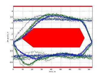
2 Abbreviations
                  •   USB:        Universal serial bus
                  •   USB IF:     USB Implementation Forum
                  •   FS:         USB full speed (12Mbit/s)
                  •   LS          USB low speed (1.5MBit/s)
                  •   HS:         USB high speed (480MBit/s)
                  •   PCB:        Printed circuit board
                  •   EFTB:       Electrical fast transient burst
                  •   DP or D+:   Data Plus differential line
                  •   DM or D-:   Data Minus differential line
                  •   DFLL:       Digital frequency locked loop
                  •   BOM:        Bill of materials

 2    Atmel AVR1017
                                                                    8388A-AVR-07/11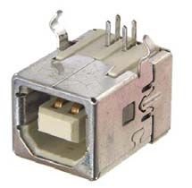
Atmel AVR1017

3 Global hardware USB requirements
                                  The USB interface consists of a differential data pair (DP/DM) and a power supply
                                  (VBUS, GND).
                                  VBUS provides a 5V power supply to optionally power the target application.
                                  The DP/DM differential pair operates at 3.3V for LS and FS devices, while HS devices
                                  use a lower voltage. As the XMEGA USB module implements FS and LS modes only,
                                  the rest of this document will not deal with USB HS mode. For FS and LS modes, the
                                  3.3V differential pair voltage is within the XMEGA power supply range. Thus, to allow
                                  USB operation, the XMEGA should be powered at 3.3V.

3.1 Power schemes
                                  According to USB specifications, USB devices can either be “bus-powered” or “self-
                                  powered.”

3.1.1 Self-powered applications
                                  Self-powered applications provide their own power supply; they are not allowed under
                                  any condition to draw any current from the USB interface.

3.1.2 Bus-powered applications
                                  Bus-powered applications draw their power supply from the 5V VBUS signal. The
                                  maximum current allowed depends on the USB mode.

3.1.2.1 Suspend mode
                                  The USB host controller may decide to enter suspend mode at any time to reduce
                                  power consumption (system sleep or standby). While in this mode, the entire
                                  application should reduce power consumption to less than 2.5mA. This means that
                                  the entire device should be able to reach this minimal static power consumption. This
                                  requires the application design to:
                                  • Reduce the number of permanent pull-up signals
                                  • Minimize or eliminate power-on LEDs
                                  • Reduce the power consumption of external components/resources (through chip
                                    select and power reduction lines, and by shutting down unused power supplies)
        NOTE                      When computing global suspend current, remember that the USB device requires
                                  keeping its DP or DM pull-up active.

3.1.2.2 Operating mode
                                  While in USB operational mode, the maximum current that can be drawn from VBUS
                                  depends on the device type and state. The device is not allowed to draw more than
                                  100mA until it is properly enumerated by the USB host. The maximum current a
                                  device can draw once enumerated is given during the enumeration process. The
                                  current ranges are from 0 to 100mA for ‘low-power’ devices, or 0 to 500mA for ‘high-
                                  power’ devices.

3.1.3 Inrush current
                                  The USB 2.0 specification states: “The maximum load (CRPB) that can be placed at
                                  the downstream end of a cable is 10μF in parallel with one unit load (100mA). The

                                                                                                                     3
 8388A-AVR-07/11
10μF capacitance represents a bypass capacitor directly connected across the VBUS
lines in the function, plus any capacitive effects visible through the regulator in the
device.”
As a result, the maximum direct capacitance allowed on the VBUS signal should be
limited to 10µF, which represents an allowable load of approximately 50µC.
According to the USB-IF: “Inrush current is measured for a minimum of 100
milliseconds (ms) after attach. Attach is defined at the moment the VBus and ground
pins of the plug mate with the receptacle. Any current exceeding 100mA during the
100ms interval is considered part of the inrush current event. The inrush current is
divided into regions. A region is an interval where the current exceeds 100mA until
the time the current falls below 100mA for at least 100µs. There can be multiple
inrush regions during the 100ms period. Pass/fail is determined by the region having
the highest charge.”
Figure 3-1. Inrush current measure.
For more detail about inrush current compliance, refer to the official USB-IF
compliance update page (http://compliance.usb.org).
3.1.4 Back-drive voltage
A USB self-powered device has its own independent power supply, as this kind of
application can operate while disconnected or not using the USB interface. The USB
specification states that the USB lines of such a device should not present any
voltage on DP, DM, or VBUS while disconnected from the bus.
4 Atmel AVR1017
8388A-AVR-07/11Atmel AVR1017
As a consequence, a USB self-powered device should implement a mechanism to
detect the USB connection state (via VBUS signal monitoring) to ensure it does not
enable its DP or DM pull-up on the differential data pair.
3.2 Signal integrity
The USB 2.0 full speed electrical specification requires some precautions to ensure
correct signal integrity.
Incorrect signal quality could make the USB device’s behavior unstable and not
compliant with the USB specification.
During USB certification, the USB signal quality is measured by performing the eye
diagram test. Figure 3-2 illustrates a correct (USB-compliant) and an incorrect eye
diagram. The incorrect one may result of improper routing or unmatched impedance
of the USB differential lines.
Figure 3-2. USB eye diagrams.
3.2.1 USB signal routing
The impedance of the differential data line pair is 90Ω to each other and 45Ω to
ground, and the termination of the line in the device may require serial resistors.
These serial resistors are included within the AVR XMEGA device. To ensure proper
signal integrity, the two DP/DM signals must be closely routed on the PCB:
• The impedance of the pair should be matched on the PCB to minimize reflections
• USB differential tracks should be routed with the same characteristics (length,
number of vias, etc.)
• Signals should be routed as parallel as possible, with a minimum number of
angles and vias
5
8388A-AVR-07/11Figure 3-3. Typical USB layout connections.
USB
Connector
RC filter
shield/GND ESD
Suppressors
USB
differential
pair
3.2.2 Clock source selection
The 12Mbit/s USB FS signal rate specification requires 0.25% accuracy. In addition,
the data recovery mechanism requires an internal ×4 oversampling mechanism.
Thus, the device should be able to generate an accurate, 48MHz signal clock to the
USB module.
To ensure proper signal quality, the Atmel AVR XMEGA provides different ways to
generate the 48MHz oversampling frequency:
• External crystal and the on-chip PLL
• Internal RC oscillator
The most convenient method is to use the on-chip, 32MHz RC oscillator calibrated at
48MHz. To ensure 0.25% signal rate accuracy, the internal RC oscillator should be
auto-calibrated using an internal DFLL. This solution allows the external BOM cost to
be reduced (no need for an external crystal).
NOTE The USB module for XMEGA requires a minimum 12MHz CPU clock to send and
receive data. Be sure to configure the XMEGA system clock with a minimum 12MHz
clock when using the USB module. This clock can be stopped when USB is in
suspend mode.
3.3 Bus connection
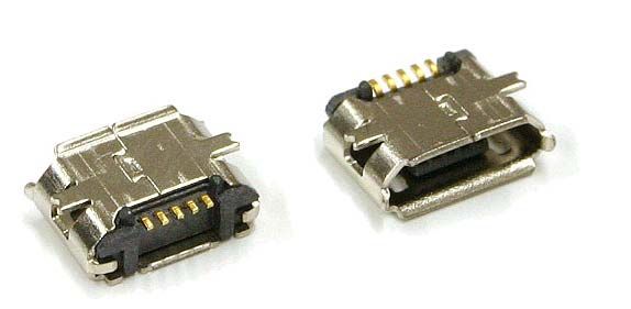
3.3.1 Connector types
The device can be connected to the host via a captive cable or by using a soldered
receptacle with a USB cable.
For USB device connection, the USB specification states that one and only one USB
connector can be used. It can be one of the following:
6 Atmel AVR1017
8388A-AVR-07/11Atmel AVR1017
• B receptacle
• Mini-B receptacle
• Micro-B receptacle
When applying for USB device certification, be sure to use a certified USB connector
listed by the USB-IF. Certified USB connectors can be found from the USB-IF product
search web page (http://www.usb.org/kcompliance/view).
Be sure to use properly shielded USB cable when using a captive cable in FS mode,
and limit the cable length to 1.5m in LS mode.
3.3.2 Electrostatic protection
USB allows the application to have an open connection to the external environment,
which could expose the entire system to ESD.
Even though Atmel AVR XMEGA devices embed on-chip ESD protection, it is
recommended to increase ESD protection on the USB DP, DM, and VBUS lines using
dedicated transient suppressors. These protections should be located as close as
possible to the USB connector to reduce the potential discharge path and reduce
discharge propagation within the entire system.
Figure 3-4. Typical USB ESD protections.
VBUS
D+
D-
GND
ESD Suppressors
SHIELD
7
8388A-AVR-07/11The ESD suppressors can be independent, discrete protection devices or specific,
integrated USB protections.
3.3.3 EMI considerations
The USB FS cable includes a dedicated shield wire that should be connected to the
board with caution. Special attention should be paid to the connection between the
board ground plane and the shield from the USB connector and the cable.
Tying the shield directly to ground would create a direct path from the ground plane to
the shield, turning the USB cable into an antenna. To limit the USB cable antenna
effect, it is recommended to connect the shield and ground through an RC filter.
Typically, R = 1MΩ and C = 4.7nF in Figure 3-5.
Figure 3-5. Typical shield and ground connection.
8 Atmel AVR1017
8388A-AVR-07/11Atmel AVR1017
4 Typical USB applications with Atmel XMEGA
Atmel XMEGA devices with USB modules now make the implementation of USB
connectivity easy by reducing external component needs:
• On-chip USB serial resistors
• On-chip USB pull-up resistor
• No need for an external crystal, because AVR XMEGA can achieve USB FS and
LS communication using its internal RC oscillator
4.1 Power supply considerations
The USB differential pair operates at, typically, 3.3V. As a result, to comply with the
USB specifications, the AVR XMEGA device should be powered with VCC = 3.3V.
4.2 Bus-powered application
When designing bus-powered applications, power management is critical. The AVR
XMEGA offers a wide range of power saving modes to achieve the lowest possible
power consumption for the system. However, some special considerations should be
taken into account regarding external component selection. As explained before, bus-
powered applications use the 5V VBUS power supply to feed the entire application.
An external low dropout regulator is required to generate the 3.3V AVR XMEGA
power supply.
When selecting this regulator, be sure its quiescent current does not consume too
large a proportion of the global 2.5mA suspend current.
Figure 4-1. Bus power scheme connection.
4.3 VBUS detection for self-powered devices
Self-powered devices require a way to detect the USB connection status by
monitoring the VBUS signal. This could be achieved using a basic resistor voltage
divider.
Figure 4-2. Self-power scheme connection.
9
8388A-AVR-07/115 Conclusion
Within the past years, USB has become a standard and an easy-to-use
communication interface. Atmel AVR XMEGA devices provide an efficient USB
solution to integrate USB in most applications. But designing an application that fully
complies with the USB specifications requires careful attention to several issues.
Table 5-1 summarizes the technical issues and their potential solutions.
Table 5-1. Summary of USB hardware requirements.
Technical issue Recommendation
- Use an appropriate power reduction mode in USB suspend
mode
Power management - Select a regulator with a low quiescent current
- Reduce consumption of all external resources (LEDs, pull-up,
chip select, etc.)
- Use certified connectors and cables
- USB differential pair routing
USB signal quality
- Source clock selection
- Power supply quality
- ESD suppressors on VBUS, D+, and D- located close to the USB
ESD
connector
EMC - Indirect ground/shield connection
- Maximum VBUS equivalent capacitance should be lower than
Inrush current
10µF
Back-drive voltage - VBUS signal monitoring required to control USB attachment
10 Atmel AVR1017
8388A-AVR-07/11Atmel AVR1017
6 Table of contents
Features ............................................................................................... 1
1 Introduction ...................................................................................... 1
2 Abbreviations ................................................................................... 2
3 Global hardware USB requirements............................................... 3
3.1 Power schemes ................................................................................................... 3
3.1.1 Self-powered applications ......................................................................................... 3
3.1.2 Bus-powered applications ......................................................................................... 3
3.1.3 Inrush current ............................................................................................................ 3
3.1.4 Back-drive voltage ..................................................................................................... 4
3.2 Signal integrity ..................................................................................................... 5
3.2.1 USB signal routing..................................................................................................... 5
3.2.2 Clock source selection............................................................................................... 6
3.3 Bus connection .................................................................................................... 6
3.3.1 Connector types ........................................................................................................ 6
3.3.2 Electrostatic protection .............................................................................................. 7
3.3.3 EMI considerations .................................................................................................... 8
4 Typical USB applications with Atmel XMEGA ............................... 9
4.1 Power supply considerations............................................................................... 9
4.2 Bus-powered application ..................................................................................... 9
4.3 VBUS detection for self-powered devices........................................................... 9
5 Conclusion ..................................................................................... 10
6 Table of contents ........................................................................... 11
11
8388A-AVR-07/11Atmel Corporation Atmel Asia Limited Atmel Munich GmbH Atmel Japan
2325 Orchard Parkway Unit 01-5 & 16, 19F Business Campus 9F, Tonetsu Shinkawa Bldg.
San Jose, CA 95131 BEA Tower, Milennium City 5 Parkring 4 1-24-8 Shinkawa
USA 418 Kwun Tong Road D-85748 Garching b. Munich Chou-ku, Tokyo 104-0033
Tel: (+1)(408) 441-0311 Kwun Tong, Kowloon GERMANY JAPAN
Fax: (+1)(408) 487-2600 HONG KONG Tel: (+49) 89-31970-0 Tel: (+81) 3523-3551
www.atmel.com Tel: (+852) 2245-6100 Fax: (+49) 89-3194621 Fax: (+81) 3523-7581
Fax: (+852) 2722-1369
© 2011 Atmel Corporation. All rights reserved.
® ® ® ®
Atmel , Atmel logo and combinations thereof, AVR , AVR logo, XMEGA , and others are registered trademarks or trademarks of Atmel
Corporation or its subsidiaries. Other terms and product names may be trademarks of others.
Disclaimer: The information in this document is provided in connection with Atmel products. No license, express or implied, by estoppel or otherwise, to
any intellectual property right is granted by this document or in connection with the sale of Atmel products. EXCEPT AS SET FORTH IN THE ATMEL
TERMS AND CONDITIONS OF SALES LOCATED ON THE ATMEL WEBSITE, ATMEL ASSUMES NO LIABILITY WHATSOEVER AND DISCLAIMS
ANY EXPRESS, IMPLIED OR STATUTORY WARRANTY RELATING TO ITS PRODUCTS INCLUDING, BUT NOT LIMITED TO, THE IMPLIED
WARRANTY OF MERCHANTABILITY, FITNESS FOR A PARTICULAR PURPOSE, OR NON-INFRINGEMENT. IN NO EVENT SHALL ATMEL BE
LIABLE FOR ANY DIRECT, INDIRECT, CONSEQUENTIAL, PUNITIVE, SPECIAL OR INCIDENTAL DAMAGES (INCLUDING, WITHOUT LIMITATION,
DAMAGES FOR LOSS AND PROFITS, BUSINESS INTERRUPTION, OR LOSS OF INFORMATION) ARISING OUT OF THE USE OR INABILITY TO
USE THIS DOCUMENT, EVEN IF ATMEL HAS BEEN ADVISED OF THE POSSIBILITY OF SUCH DAMAGES. Atmel makes no representations or
warranties with respect to the accuracy or completeness of the contents of this document and reserves the right to make changes to specifications and
product descriptions at any time without notice. Atmel does not make any commitment to update the information contained herein. Unless specifically
provided otherwise, Atmel products are not suitable for, and shall not be used in, automotive applications. Atmel products are not intended, authorized, or
warranted for use as components in applications intended to support or sustain life.
8388A-AVR-07/11You can also read