Optical Signatures of Defect Centers in Transition Metal Dichalcogenide Monolayers - ORBi
←
→
Page content transcription
If your browser does not render page correctly, please read the page content below
COMMUNICATION
 www.advquantumtech.com

Optical Signatures of Defect Centers in Transition Metal
Dichalcogenide Monolayers
Pedro Miguel M. C. de Melo,* Zeila Zanolli, and Matthieu J. Verstraete

 and the presence of strongly bound exci-
Even the best quality 2D materials have non-negligible concentrations of tons, opening avenues for next generation
vacancies and impurities. It is critical to understand and quantify how defects opto-electronics.[1,2] Manufactured samples
change intrinsic properties, and use this knowledge to generate functionality. have strongly improved in quality, but will
This challenge can be addressed by employing many-body perturbation theory always contain a significant concentration
 of defects.[3,4] Graphene can be crystallized
to obtain the optical absorption spectra of defected transition metal
 almost perfectly in very large flakes, but
dichalcogenides. Herein metal vacancies, which are largely unreported, show TMDs present many more natural defects,
a larger set of polarized excitons than chalcogenide vacancies, introducing in particular chalcogen vacancies (see e.g.,
localized excitons in the sub-optical-gap region, whose wave functions and Ref. [5]). On the bright side, defects and
spectra make them good candidates as quantum emitters. Despite the strong substitutional dopants can be used to tune
 the electronic structure and optical prop-
interaction with substitutional defects, the spin texture and pristine exciton
 erties of materials.[6] By doing so, devices
energies are preserved, enabling grafting and patterning in optical detectors, sensitive to specific wavelengths and po-
as the full optical-gap region remains available. A redistribution of excitonic larizations can be engineered (reviewed in
weight between the A and B excitons is visible in both cases and may allow Ref. [7]), and can even behave as single pho-
the quantification of the defect concentration. This work establishes excitonic ton emitters.[8] There is an ongoing search
signatures to characterize defects in 2D materials and highlights vacancies as for long lived spin states at room temper-
 atures in TMDs. Here defects are expected
qubit candidates for quantum computing.
 to play a crucial role in both scattering and
 storing spin information - we showed re-
 cently that intrinsic scattering mechanisms
Transition metal dichalcogenides (TMDs) have become strong (the electron-phonon interaction) can quickly destroy the
contenders for the engineering of optical devices, especially pumped spin-polarization.[9] Chalcogen vacancies can also be
thanks to their coupling of the spin and valley degrees of freedom, used as grafting sites for functional groups, to create bio and
 chemical sensors.[10,11] Alkane and other functional groups can
 be incorporated directly into the matrix (as opposed to thiol links,
Dr. P. M. M. C. de Melo, Prof. M. J. Verstraete
nanomat/Q-mat/CESAM
 for instance, which necessitate Au). Carbon atoms have also been
Université de Liège used as acceptor dopants for bulk semiconductors.[12] In TMDs,
Institut de Physique mixed phases with transition metal carbides have been shown to
B-4000 Sart Tilman, Liège, Belgium have applications in catalysis,[13,14] while in MoS2 it was shown
E-mail: p.m.monteirocamposdemelo@uu.nl that carbon substitutions had a strong effect on the TMD elec-
Dr. P. M. M. C. de Melo, Prof. Z. Zanolli tronic and optical properties.[15,16]
Chemistry Department
Debye Institute for Nanomaterials Science Many experiments give access to the presence and proper-
Condensed Matter and Interfaces ties of localized defects. In TMDs the most commonly used are:
Utrecht University scanning tunneling microscopy which shows contrast changes
PO Box 80.000, 3508 TA Utrecht, The Netherlands due to chemical substitution and electron cloud reconstruc-
Prof. Z. Zanolli tion around defects;[17] scanning tunneling spectroscopy, which
Catalan Institute of Nanoscience and Nanotechnology (ICN2)
CSIC and BIST
 probes the detailed electronic structure at the defect site;[17] op-
Campus UAB, Bellaterra, Barcelona 08193, Spain tical spectroscopy showing absorption and photoluminescence
Dr. P. M. M. C. de Melo, Prof. Z. Zanolli, Prof. M. J. Verstraete by the defect-induced states;[18–20] tunneling transport from in-
European Theoretical Spectroscopy Facility (ETSF) www.etsf.eu sulated contacts through a core material, which is resonant
 through defect states in the core band gap;[19] transmission
 The ORCID identification number(s) for the author(s) of this article
 can be found under https://doi.org/10.1002/qute.202000118
 electron microscopy, which gives both structural and chemical
 information.[3,21]
© 2021 The Authors. Advanced Quantum Technologies published by
Wiley-VCH GmbH. This is an open access article under the terms of the Understanding how defects affect optical properties is a first
Creative Commons Attribution License, which permits use, distribution essential step toward controlled functionalization of materi-
and reproduction in any medium, provided the original work is properly als, both for fingerprinting (optical characterization is simple,
cited. remote, and non-destructive) and to understand derived opti-
DOI: 10.1002/qute.202000118 cal functionalities. First-principles computational techniques

Adv. Quantum Technol. 2021, 4, 2000118 2000118 (1 of 8) © 2021 The Authors. Advanced Quantum Technologies published by Wiley-VCH GmbH
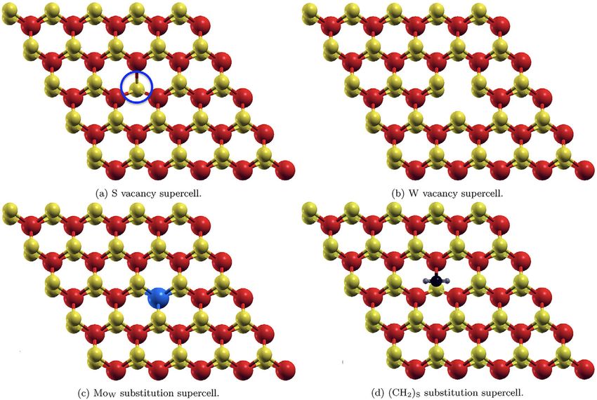
www.advancedsciencenews.com www.advquantumtech.com

Figure 1. Defected 5×5 supercells used in this work. a) S vacancy, marked by the blue circle. b) W vacancy. c) MoW substitution. d) (CH2 )S substitution.
Tungsten atoms are shown in red, sulfur in yellow, molybdenum in blue, carbon in black, and hydrogen in grey.

provide a high degree of physical insight and predictive power tive gaps. Since bulk states are the dominant contribution to elec-
in the spectral features of defects, to find new peaks and yield tronic screening, we expect that our results are also indicative of
quantitative positions and weight transfers. the behavior of charged defects. We analyze the resulting changes
 Several methods can be used to generate defects in layers of in electronic band structure and optical absorption spectra, aim-
TMDs: in situ defects can be created by either chemical vapor ing to answer the question: can we identify a defect, and ideally
transport (CVT) or chemical vapor deposition, which allow for quantify its concentration,[22] just by looking at the absorption
some degree of control in the generation of substitutional de- spectrum? While chalcogen vacancies have been subject to some
fects or chalcogenide vacancies during the synthesis of the sys- studies,[22] metal vacancies and isovalent substitutions like MoW
tem; techniques such as electron beam irradiation, ion bombard- and (CH2 )S are still largely unreported, limiting our knowledge
ment, plasma treatment, thermal annealing, ozone treatment, of their behavior as quantum emitters or chemical detectors. We
and laser illumination can be used to create ex situ defects.[7] find that defects fall into two functional categories, based on the
The four point defects we present in this work, S vacancy, W presence of bound states within the band-gap of WS2 . We discuss
vacancy, MoW substitution, (CH2 )S substitution, are thus a rep- their spectra, spin textures and the criteria which could be used
resentative sample of different systems that can be of interest to identify each defect.
in the near future. While some studies on the optical response In Figure 1 we show the four defects that are the focus of
of defected TMD supercells exist,[22–24] here we present a rep- our work: two vacancies (S and W ions); and two substitutions,
resentative sample of highly converged calculations on defects MoW and (CH2 )S . The S vacancy is the most commonly found
that have shown potential due to their ease in manufacturing (S defect in monolayers of WS2 and often assigned to specific fea-
vacancy, MoW substitution, (CH2 )S substitution) or rich optical tures below the optical gap.[18] In the substitution case MoW
features (W vacancy). However, multiple types of point defects is quite commonly found in nature, and carbon is a common
can be present in the sample, coming from the synthesis process dopant in semiconductors.[25] Studies have been made on the
or subsequent treatments. If these defects add new states to the potential transport applications of TMDs and transition metal
mid-gap region, it could complicate the identification of defects carbides.[13,26] In the case of MoS2 experiments point to changes
from optical measurements, depending on their line-widths and to the electronic structure due to carbon doping, which should
experimental resolution. Further research should look into the translate into new optical features.[15,27]
most common defects introduced during sample treatment after In ideal defect engineering, induced changes in the system
synthesis and their effects on optical response. should yield new controllable features that are distinct from the
 In this work, we present a fully First-principles investigation of pristine properties. In the case of TMDs, a key property that re-
charge-neutral defected monolayers of WS2 , based on the Bethe– lates to optics is the polarization of states at the K wave vector
Salpeter equation (BSE) for electron–hole interactions within in the Brillouin zone. The polarization will control the allowed
many body perturbation theory. In Ref. [22] it has been shown optical transitions that form bright excitons. We label in order of
that charging a defect in TMDs mainly changes the absolute en- increasing energy the last two occupied states and the first two
ergies of defect states, but almost not their number or their rela- unoccupied states at K as (v1 , v2 , c1 , c2 ). For pristine WS2 (see the

Adv. Quantum Technol. 2021, 4, 2000118 2000118 (2 of 8) © 2021 The Authors. Advanced Quantum Technologies published by Wiley-VCH GmbH
www.advancedsciencenews.com www.advquantumtech.com

Figure 2. a,c) DFT band structures and spin-texture of defected WS2 for the S and W vacancies, respectively. Color scale indicates value of ⟨Sz ⟩ (red for
1 and blue for −1). The Fermi level is set to the last occupied state and shaded regions indicate the bulk region. In both cases new states arise in the
mid-gap region. Two occupied defect states are visible in the band structure of the W vacancy. b,d) Optical absorption spectra of the S and W vacancies,
respectively. The spectra are cut at 2.5 eV, as higher energy bands were not included in the BSE kernel. Calculations were converged to reproduce A and
B bulk exciton peaks. Absorption of the pristine system is shown in grey. The positions of the first excitonic peaks are shown by vertical lines. Labels
and vertical lines have matching colors. Two new peaks arise for the S vacancy due to the two new manifolds of mid-gap states. The W vacancy exhibits
several new peaks, as four new manifolds of defect states arise. The outsets in (b) and (d) show the level scheme and main excitonic transitions.

Supporting Information for more information), the first bright defect states are allowed, with different oscillator strengths and
exciton would be made of an optical transition from v2 to c2 , different excitation energies.
while the second brightest exciton would be made by a transition The W vacancy is more challenging numerically: the defect
from v1 to c1 . This is due to the fact that optical selection rules bands are split off from the bulk conduction and valence bands,
enforce spin conservation in TMDs: the valence and conduction but in the 5×5 supercell they still show some dispersion and a
manifold differ in orbital character, guaranteeing the needed an- finite band width. Their position and spin texture are close to
gular momentum change when absorbing a helical photon.[28] what has been found in other DFT calculations for this defect
 We start by analyzing two systems which feature states in the using larger supercells,[16] and we extract a semi-quantitative pic-
pristine band gap: the sulfur and tungsten vacancies. Their DFT ture of the optical properties. Together with the six new mid-gap
band structures are shown in Figure 2a,c, respectively. Note that states, there are also four new occupied states bound to the de-
using a 5×5 supercell, the point K of the pristine Brillouin zone fect in the valence region (unlike the S vacancy). All these states
(BZ) folds back into the point K of the supercell BZ. are spin polarized at K, so if we consider optical selection rules,
 Both systems preserve the spin polarization of pristine states we can expect new peaks to show up in the absorption spectrum.
at K, meaning that the A and B peaks that are the dominant fea- These peaks will be a combination of transitions between pris-
tures of the pristine spectrum must also be present. For the S tine and defect states, and others between defect states (occupied
vacancy, Figure 2a, new non-dispersive mid-gap singlet states ap- to empty) in the mid-gap region.
pear 1.08 and 1.28 eV above the valence band edge, in agreement The effects of changes in the band structure on the BSE optical
with what was previously found.[16,29] At K the first band is almost spectrum are shown in Figure 2. For comparison the absorption
completely spin-unpolarized, while the second is completely po- spectrum of the pristine system is shown in grey. The energies
larized. This opens a path for new emission channels, as elec- of all identified excitons are listed in Table S1, Supporting Infor-
tronic transitions from the pristine valence states to these new mation, along with the reference energies for the pristine case.

Adv. Quantum Technol. 2021, 4, 2000118 2000118 (3 of 8) © 2021 The Authors. Advanced Quantum Technologies published by Wiley-VCH GmbH
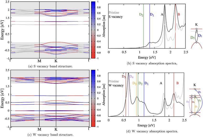
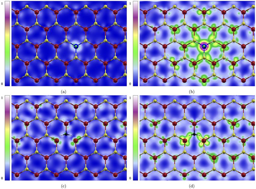
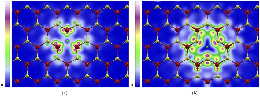
www.advancedsciencenews.com www.advquantumtech.com

Figure 3. a) S vacancy wave function for excitonic state D2 , shown in Figure 2b. b) W vacancy wave function for excitonic state D5 , shown in Figure 2d.
The hole is marked by the green sphere and it is placed at the position of the missing sulfur ion. In both cases the electronic charge is highly localized
near the hole, indicating the formation of a quantum dot.

Note in passing that the higher energy peaks beyond A and B are each exciton. For D3 and D5 , their relative intensities with respect
not reproduced in full in our calculations, due to limitations in to exciton A are 0.47 and 0.76, respectively. For the exciton state
the number of states included in the BSE for such large systems. D4 , the relative intensity is 1.88. However, this exciton state still
 With an S vacancy in Figure 2a two new peaks arise at 1.35 suffers from contaminating interactions coming from adjacent
and 1.14 eV due to the mid-gap states. They are marked D1 and vacancy sites, resulting from the size of the supercell used in our
D2 in Figure 2b. As shown in the inset, D1 and D2 correspond to calculations. Table S2, Supporting Information shows all the rel-
optical transitions from the top valence band to the defect state ative intensities of each exciton state with respect to the A exciton
at 1.28 and 1.08 eV, respectively. However, since the lowest defect for all systems.
state is not fully polarized, the resulting dipole matrix element is A more detailed analysis to the excitonic wave functions shows
much smaller than that of the D1 peak, where the defect state is that two of the low intensity peaks (D1 and D3 ) are artifacts due
fully polarized. to the interaction of defect states in neighboring periodic repli-
 The exciton wave function for the peak corresponding to D1 cas. They result from electron-hole pairs localized on different
is shown in Figure 3a. Here the hole is placed at the position vacancy sites (see Figure S7, Supporting Information for zoomed
of the vacant sulfur ion (marked by the green sphere) and the out plots of excitonic wave function). The majority of the elec-
magnitude on the color-map shows the probability density of the tronic charge in the exciton is not localized near the same ion
electron (see the Figure S5, Supporting Information where all the vacancy as the hole, and is bound thanks to a finite overlap of
excitonic wave functions are depicted). The color map shows that the DFT defect state wavefunctions. These two peaks will disap-
exciton states are highly localized on the neighboring tungsten pear if larger supercells are used: the dipole matrix element and
atoms, indicating that the S vacancy does indeed form a quan- oscillator strength will go do 0. We note that while the BSE is
tum dot. solved only for q = 0, the introduction of non-dispersive defect
 For the W vacancy, whose spectrum is shown in Figure 2d, states allows for many transitions to occur throughout the BZ, so
more peaks are present due to the increased number of defect an exciton function can actually be composed of several vertical
states. In total we identify five excitons: three composed from transitions at different momenta (NB: this is distinct from a finite
holes in the valence band and electrons in defect states, D1 to wave vector for the whole exciton).
D3 ; and two others with both the electron and the hole bound to In the case of D2 , shown in Figure S7, Supporting Information,
two different manifolds of defect states, D4 and D5 . The states there is a residual interaction with adjacent vacancy sites, but now
involved in the formation in the excitons are shown in the in- the hole is correctly bound to an electron located at the same site.
set of Figure 2d. The most striking feature is the relative inten- For D5 , shown in Figure 3b both the electron and hole are entirely
sity of the D4 and D5 excitons relative to the A and B excitons. located at the same site.
As defect states have very weak dispersion, the associated elec- We note that hybridization between bulk and defect exciton
trons and holes will have large effective masses. It is possible to states is not expected to occur in systems with low defect density.
show[30] that oscillator strengths are proportional to the reduced In the case of our calculations all wave-functions are orthogonal
mass of electron and hole, which explains why the effect is fur- by construction, and for larger supercells any overlap between
ther magnified for transitions between defect states in the case pristine and defect excitons should vanish.
of the W vacancy. The two vacancies thus show very distinct optical signa-
 The high intensity shown in Figure 2d for exciton states D3 , tures, coming from the different richness in defect states that
D4 , and D5 is an artifact and results mainly from the overlapping arise in their band structures. This, together with the changes
of the Lorentzian functions used to plot the peaks associated with in the intensity due to different levels of defect density (see

Adv. Quantum Technol. 2021, 4, 2000118 2000118 (4 of 8) © 2021 The Authors. Advanced Quantum Technologies published by Wiley-VCH GmbH
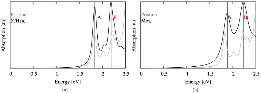
www.advancedsciencenews.com www.advquantumtech.com

Figure 4. Optical absorption spectra for the 5×5 supercells with the a) (CH2 )S substitution; b) MoS2 substitution. Absorption of the pristine system is
shown in grey. The positions of the first excitonic peaks are shown by vertical lines. Labels and vertical lines have matching colors. Both cases show no
new peaks, with the A and B excitons at energies that almost match those of the pristine case. The spectra are cut at 2.5 eV, as higher energy bands were
not included in the BSE kernel. Calculations were converged to reproduce the A and B bulk exciton peaks.

Figure S10, Supporting Information) indicate that even at low of our supercell sizes). If experimental precision is on this level
densities it should be possible to distinguish between a sulfur the main spectral signature for MoW is the blue shift of the A
and a tungsten vacancy just through measuring the optical ab- peak and the broadening of both peaks. However, many other
sorption of the sample. (especially isovalent) defects may have similar manifestations.
 We studied two cases of substitutions in the WS2 monolayer; We can now establish a more complete picture of how different
one with a molybdenum atom replacing a tungsten atom; and an- defects change optical properties of TMDs. The main changes to
other where a sulfur atom was replaced by a methyl, the simplest the optical spectrum come from new mid-gap states. Isovalent
(divalent) group representing grafted organic substituents. substitutions like MoW and (CH2 )S will not be trivially seen in
 In both cases no mid gap states where found (see Figure S4, the absorption spectra, but can still be detected by the ratio of
Supporting Information for their bandstructures), which can be the A and B peak intensities, and by localization in the exciton’s
rationalized as follows. In the case of MoW substitution, molyb- spatial distribution.
denum and tungsten have the same valence, close atomic and In terms of potential applications, the two vacancies are clear
covalent radii,[31–33] resulting in similar chemical properties. A front runners for designing quantum dots and quantum emit-
small concentration of defects does not lead to strong changes in ters. In particular the S vacancy has already shown some promis-
the charge density, thus leaving the system practically unchanged ing results as a single photon emitter.[35] The two mid-gap
when compared to the pristine case. For the (CH2 )S substitution, defect states are actively considered for quantum computing
the methylene group provides the same number of valence elec- applications: they are separated in energy by 0.21 eV, mak-
trons as the sulfur atom. The breaking of local symmetry is not ing them addressable using mid-infrared lasers, and insulating
strong enough to perturb the band edges. them from the highest phonon energy in pristine WS2 , which is
 The lack of mid-gap states is reflected in the absorption spectra 53 meV.[36,37]
shown in Figure 4. In both cases the excitonic peaks lie almost The W vacancy offers a larger set of localized excitons, but is
on top of those of the pristine system, with the largest deviation more energetic and harder to produce (see Table S1, Supporting
being 60 meV for the MoW A peak. The energies for the defected Information). Here the brightest excitons are made of transitions
A and B peaks are shown in Table S1, Supporting Information. between single particle defect states, due to their large effective
 There is, however, both weight transfer and changes in spin masses. These exciton states show potential in devices as they
texture for the A and B peaks at higher energies in the absorp- would behave as bright emitters with multiple internal states,
tion spectrum of both substitutions, which leaves some hope to behaving like an embedded molecule for multivalued quantum
identify these defects experimentally. The strongest signature of computing.[38] The residual band width will disappear only in a
the substitution lies within the exciton wave functions shown in 7×7 supercell,[16] but the spin texture and qualitative features are
Figure 5. While the exciton cloud is still dispersed throughout the already well represented here (see Figure S3, Supporting Infor-
crystal, there is a higher charge concentration near the substitu- mation). In actual samples, this vacancy type is more likely to be
tion. In the (CH2 )S case this is valid for the A exciton (Figure 5c), charged, with electrons filling the dangling S ion’s orbitals.
and in MoW both A and B excitonic states localize near the de- We have shown that the isovalent substitutions MoW and
fect. The (CH2 )S case also shows breaking of C3 symmetry by (CH2 )S will not produce in-gap states. Though this is intuitive,
the methyl molecule. The localization is due both to the defect- it is not trivial, and the local electronic structure is strongly mod-
related electronic states and to the choice of the initial position ified as shown by the excitonic wave functions. For purposes of
of the hole. For reference, in boron nitride similar extensions of grafting organic molecules, this means the full band gap window
3–5 nearest neighbors are found in Ref. [34]. of intrinsic WS2 will be available for optical sensing.
 The two peaks which correspond to the bulk excitons A and In conclusion, we employ powerful and accurate first princi-
B known from literature, and are within 50 meV of those of the ples techniques to shed some light into the changes in optical
pristine system in all cases (this is below the absolute precision properties introduced by point defects in TMDs. Two promis-
of the first principles methods, and shows the basic convergence ing systems, S and W ion vacancies, have potential for quantum

Adv. Quantum Technol. 2021, 4, 2000118 2000118 (5 of 8) © 2021 The Authors. Advanced Quantum Technologies published by Wiley-VCH GmbH
www.advancedsciencenews.com www.advquantumtech.com

Figure 5. The A (left column) and B (right) excitonic wave functions of a,b) MoW and c,d) (CH2 )S , shown in Figure 4. The hole is marked by the green
sphere and it is placed between the mid-plane and the carbon ion. While there is some charge localization and symmetry breaking, the exciton wave
function extends through the whole system.

emitters and even quantum computing. While W vacancies are wave kinetic energy cutoff of 95 Ry was used, with a tolerance
the least energetically favorable, it is the one with the richest and parameter of 10−12 for the error in the density. The forces on the
most interesting variety of defect bound excitons. Such defects atoms were converged down to 10−5 Ry bohr−1 and the minimum
might be possible to synthesize in environments with lower con- difference in total energies was set to 10−8 Ry to achieve structural
centrations of tungsten or focused TEM beams. Isovalent vacan- optimization. The pristine systems were computed on a 30×30 k-
cies do not introduce mid-gap states in the band structure, but do point mesh. Therefore, a mesh of 6×6 k-points was sufficient for
change the relative intensity of the canonical A and B peaks, and modeling the 5×5 supercells.
the spatial distribution of the first and second excitonic states, G0 W0 corrections of the ground state electronic structure
in the (CH2 )S case even leading to a breaking of symmetry. In were computed in the plasmon–pole approximation, using the
both cases the full sub optical gap region is available for use Yambo code.[41] A total of 1700 bands where necessary to converge
in detection of molecules that might graft themselves onto the the screening, while kinetic cut-offs of 2 Ha where used to com-
TMD’s surface. pute the integrals. This allowed for convergence within the range
 of the meV. The resulting energy level corrections were then used
Methodology Section in solving the BSE equation, as shown in Equation (1).
 The absorption spectra was computed using the Bethe–
Ground state calculations and structural optimization were per- Salpeter equation[42] as implemented in the Yambo code,[41] to
formed with the Quantum Espresso package[39] using the GGA properly account for excitonic effects. This involves solving the
exchange correlation functional. Supercells where generated by eigenvalue equation
replicating the pristine cell (previously optimized) and then in-
troducing a defect. The electrostatic isolation in the out-of-plane ( ) ∑
 GW
 ck
 − GW
 vk
 Avck + K ehvck Av ′ c′ k′ = E Avck

 (1)
direction was ensured by a Coulomb cutoff technique.[40] A plane- k′ c′ v′ v′ c′ k′

Adv. Quantum Technol. 2021, 4, 2000118 2000118 (6 of 8) © 2021 The Authors. Advanced Quantum Technologies published by Wiley-VCH GmbH
www.advancedsciencenews.com www.advquantumtech.com

where ck∕vk are quasi-particle band energies obtained from the authors thankfully acknowledge the computer resources at Mare Nos-
G0 W0 COHSEX approximation[42] and K eh accounts for the static trum technical support provided by the Barcelona Supercomputing Center
 (Spanish Supercomputing Network, RES). This publication is also based
screened and bare Coulomb interactions between electrons and
 upon work from COST Action TUMIEE (CA17126), supported by COST
holes. The excitonic wave function, | ⟩, is then constructed by (European Cooperation in Science and Technology).
using
 ∑
| ⟩ =
 Avck |ck⟩ |vk⟩ (2) Conflict of Interest
 k,c,v
 The authors declare no conflict of interest.
In the calculations the focus is on the bound exciton energies
below the band gap, so the BSE kernel only has the electron–hole Keywords
pairs needed to converge the pristine system’s first two excitons,
 defect centers, optical absorption, transition metal dichalcogenides, quan-
marked as A and B. The optical absorption was then obtained
 tum dots
directly from the imaginary part of the dielectric function, ( ),
which is given (within the Tamm–Dancoff approximation) by
 Received: October 15, 2020
 Revised: December 7, 2020
 | |
 2
 ∑ ||⟨vk − q|e−iq⋅r |ck⟩ Acvk || Published online: February 3, 2021
 ( ) = −2 lim (3)
 q→0
 ,c,v,k
 − E + i

Here c/v represent conduction/valence states, k is the k-point vec- [1] Q. H. Wang, K. Kalantar-Zadeh, A. Kis, J. N. Coleman, M. S. Strano,

tor in the Brillouin zone. , E , and Acvk are the exciton index, Nat. Nanotechnol. 2012, 7, 699.
eigenenergy and eigenvector of Equation 1. The electron–hole in- [2] K. F. Mak, J. Shan, Nat. Photonics 2016, 10, 216.
teraction is included in K eh , which contains both the un-screened [3] D. Edelberg, D. Rhodes, A. Kerelsky, B. Kim, J. Wang, A. Zangiabadi,
exchange interaction and the screened direct Coulomb interac- C. Kim, A. Abhinandan, J. Ardelean, M. Scully, D. Scullion, L. Embon,
tion. The values for kinetic cut-off parameters were equal to those R. Zu, E. J. G. Santos, L. Balicas, C. Marianetti, K. Barmak, X. Zhu, J.
 Hone, A. N. Pasupathy, Nano Lett. 2019, 19, 4371.
used during the GW-COHSEX calculations. In order to properly
 [4] N. Briggs, S. Subramanian, Z. Lin, X. Li, X. Zhang, K. Zhang, K. Xiao,
account for the bands in the same energy range as the pristine D. Geohegan, R. Wallace, L.-Q. Chen, M. Terrones, A. Ebrahimi, S.
case, a total of 60 bands were used in the BSE kernel. Das, J. Redwing, C. Hinkle, K. Momeni, A. van Duin, V. Crespi, S. Kar,
 J. A. Robinson, 2D Mater. 2019, 6, 022001.
 [5] H.-P. Komsa, J. Kotakoski, S. Kurasch, O. Lehtinen, U. Kaiser, A. V.
Supporting Information Krasheninnikov, Phys. Rev. Lett. 2012, 109, 035503.
 [6] S. Feng, Z. Lin, X. Gan, R. Lv, M. Terrones, Nanoscale Horiz. 2017, 2,
Supporting Information is available from the Wiley Online Library or from 72.
the author. [7] Z. Lin, B. R. Carvalho, E. Kahn, R. Lv, R. Rao, H. Terrones, M. A. Pi-
 menta, M. Terrones, 2D Mater. 2016, 3, 022002.
 [8] R. Bourrellier, S. Meuret, A. Tararan, O. Stéphan, M. Kociak, L. H.
 Tizei, A. Zobelli, Nano Lett. 2016, 16, 4317.
Acknowledgements [9] M. Ersfeld, F. Volmer, P. M. M. C. de Melo, R. de Winter, M. Heithoff,
The authors wish to acknowledge important input, discussions, and stim- Z. Zanolli, C. Stampfer, M. J. Verstraete, B. Beschoten, Nano Lett.
ulus from M. Terrones, B. Biel, and M. Palummo, as well as extensive sup- 2019, 19, 4083.
port from the Yambo developer team. [10] A. Bolotsky, D. Butler, C. Dong, K. Gerace, N. R. Glavin, C. Muratore,
 P.M.M.C.M. and M.J.V. acknowledge funding by the Belgian FNRS J. A. Robinson, A. Ebrahimi, ACS Nano 2019, 13, 9781.
(PDR G.A. T.1077.15, T.0103.19, and an “out” sabbatical grant to ICN2 [11] J. Azadmanjiri, P. Kumar, V. K. Srivastava, Z. Sofer, ACS Appl. Nano
Barcelona), and the Communauté Française de Belgique (ARC AIMED Mater. 2020, 3, 3116.
G.A. 15/19-09). This publication is based upon work of the MELODICA [12] L. W. Yang, P. D. Wright, V. Eu, Z. H. Lu, A. Majerfeld, J. Appl. Phys.
project, funded by the EU FLAG-ERA_JTC2017 call. The work benefited 1992, 72, 2063.
from HPC-EUROPA3 (INFRAIA-2016-1-730897) H2020 Research Innova- [13] Z. Hai, J. Du, M. K. Akbari, C. Xue, H. Xu, S. Zhuiykov, Ionics 2017,
tion Action hosted by the Theory and Simulation group at ICN2 sup- 23, 1921.
ported by the Barcelona Supercomputing Center, and from the access [14] J. Wu, L. Ma, A. Samanta, M. Liu, B. Li, Y. Yang, J. Yuan, J. Zhang, Y.
provided by ICN2 (Barcelona, Spain) within the framework of the NFFA- Gong, J. Lou, R. Vajtai, B. Yakobson, A. K. Singh, C. S. Tiwary, P. M.
Europe Transnational Access Activity (grant agreement No 654360, pro-
 Ajayan, Adv. Mater. Interfaces 2017, 4, 1600866.
posal ID 717, submitted by PMMCM). Z.Z. acknowledges support by
 [15] Q. Yue, S. Chang, S. Qin, J. Li, Phys. Lett. A 2013, 377, 1362.
the Ramón y Cajal program RYC-2016-19344 (MINECO/AEI/FSE, UE),
 [16] M. A. Khan, M. Erementchouk, J. Hendrickson, M. N. Leuenberger,
Spanish MINECO (FIS2015-64886-C5-3-P), the Severo Ochoa Program
(MINECO, SEV-2017-0706), the CERCA programme of the Generalitat Phys. Rev. B 2017, 95, 245435.
de Catalunya (Grant 2017SGR1506), the EC H2020-INFRAEDI-2018-2020 [17] B. Schuler, J.-H. Lee, C. Kastl, K. A. Cochrane, C. T. Chen, S. Refaely-
MaX Materials Design at the Exascale CoE(grant No. 824143), and the Abramson, S. Yuan, E. van Veen, R. Roldán, N. J. Borys, R. J. Koch,
Netherlands sector plan program 2019–2023. Computational resources S. Aloni, A. M. Schwartzberg, D. F. Ogletree, J. B. Neaton, A. Weber-
were provided by the Consortium des Equipements de Calcul Intensif Bargioni, ACS Nano 2019, 13, 10520.
(CECI), funded by FRS-FNRS G.A. 2.5020.11; the Zenobe Tier-1 supercom- [18] V. Carozo, Y. Wang, K. Fujisawa, B. R. Carvalho, A. McCreary, S. Feng,
puter funded by Walloon G.A. 1117545; and by PRACE DECI grants 2DSpin Z. Lin, C. Zhou, N. Perea-López, A. L. Elías, B. Kabius, V. H. Crespi,
and Pylight on Beskow (G.A. 653838 of H2020, and FP7 RI-312763). The M. Terrones, Sci. Adv. 2017, 3, e1602813.

Adv. Quantum Technol. 2021, 4, 2000118 2000118 (7 of 8) © 2021 The Authors. Advanced Quantum Technologies published by Wiley-VCH GmbH
www.advancedsciencenews.com www.advquantumtech.com

[19] T. Y. Jeong, H. Kim, S.-J. Choi, K. Watanabe, T. Taniguchi, K. J. Yee, [32] P. Pyykkö, M. Atsumi, Chem. - Eur. J. 2009, 15, 12770.
 Y.-S. Kim, S. Jung, Nat. Commun. 2019, 10, 3825. [33] P. Pyykkö, M. Atsumi, Chem. - Eur. J. 2009, 15, 186.
[20] J. Dang, S. Sun, X. Xie, Y. Yu, K. Peng, C. Qian, S. Wu, F. Song, J. Yang, [34] F. Paleari, T. Galvani, H. Amara, F. Ducastelle, A. Molina-Sánchez, L.
 S. Xiao, L. Yang, Y. Wang, M. A. Rafiq, C. Wang, X. Xu, npj 2D Mater. Wirtz, 2D Mater. 2018, 5, 45017.
 Appl. 2020, 4, 2. [35] Y. M. He, G. Clark, J. R. Schaibley, Y. He, M. C. Chen, Y. J. Wei, X. Ding,
[21] J. Hong, R. Senga, T. Pichler, K. Suenaga, Phys. Rev. Lett. 2020, 124, Q. Zhang, W. Yao, X. Xu, C. Y. Lu, J. W. Pan, Nat. Nanotechnol. 2015,
 87401. 10, 497.
[22] S. Refaely-Abramson, D. Y. Qiu, S. G. Louie, J. B. Neaton, Phys. Rev. [36] N. A. Pike, A. Dewandre, B. Van Troeye, X. Gonze, M. J. Verstraete,
 Lett. 2018, 121, 167402. Phys. Rev. Mater. 2018, 2, 63608.
[23] F. Zhang, Y. Lu, D. S. Schulman, T. Zhang, K. Fujisawa, Z. Lin, Y. [37] N. A. Pike, A. Dewandre, B. Van Troeye, X. Gonze, M. J. Verstraete,
 Lei, A. LauraElias, S. Das, S. B. Sinnott, M. Terrones, Sci. Adv. 2019, Phys. Rev. Mater. 2019, 3, 74009.
 5, 5. [38] B. Fresch, M. V. Klymenko, R. D. Levine, F. Remacle, in Computational
[24] J. Jiang, R. Pachter, S. Mou, Nanoscale 2018, 10, 13751. Matter (Eds. S. Stepney, S. Rasmussen, M. Amos), Springer, Cham
[25] Y. J. Zheng, Y. Chen, Y. L. Huang, P. K. Gogoi, M.-Y. Li, L.-J. Li, P. E. 2018, pp. 295–318.
 Trevisanutto, Q. Wang, S. J. Pennycook, A. T. S. Wee, S. Y. Quek, ACS [39] P. Giannozzi, O. Andreussi, T. Brumme, O. Bunau, M. Buongiorno
 Nano 2019, 13, 6050. Nardelli, M. Calandra, R. Car, C. Cavazzoni, D. Ceresoli, M. Cococ-
[26] J. Jeon, Y. Park, S. Choi, J. Lee, S. S. Lim, B. H. Lee, Y. J. Song, J. H. cioni, N. Colonna, I. Carnimeo, A. Dal Corso, S. de Gironcoli, P. Del-
 Cho, Y. H. Jang, S. Lee, ACS Nano 2018, 12, 338. ugas, R. A. DiStasio, A. Ferretti, A. Floris, G. Fratesi, G. Fugallo, R.
[27] A.-M. Hu, L.-l. Wang, W.-Z. Xiao, G. Xiao, Q.-Y. Rong, Comput. Mater. Gebauer, U. Gerstmann, F. Giustino, T. Gorni, J. Jia, M. Kawamura,
 Sci. 2015, 107, 72. H.-Y. Ko, A. Kokalj, E. Küçükbenli, M. Lazzeri, et al., J. Phys.: Condens.
[28] A. Molina-Sánchez, D. Sangalli, L. Wirtz, A. Marini, Nano Lett. 2017, Matter 2017, 29, 465901.
 17, 4549. [40] C. A. Rozzi, D. Varsano, A. Marini, E. K. U. Gross, A. Rubio, Phys. Rev.
[29] B. Schuler, D. Y. Qiu, S. Refaely-Abramson, C. Kastl, C. T. Chen, S. B 2006, 73, 205119.
 Barja, R. J. Koch, D. F. Ogletree, S. Aloni, A. M. Schwartzberg, J. B. [41] D. Sangalli, A. Ferretti, H. Miranda, C. Attaccalite, I. Marri, E. Can-
 Neaton, S. G. Louie, A. Weber-Bargioni, Phys. Rev. Lett. 2019, 123, nuccia, P. Melo, M. Marsili, F. Paleari, A. Marrazzo, G. Prandini, P.
 76801. Bonfà, M. O. Atambo, F. Affinito, M. Palummo, A. Molina-Sánchez,
[30] C. Hamaguchi, Basic Semiconductor Physics, Springer, Cham 2017. C. Hogan, M. Grüning, D. Varsano, A. Marini, J. Phys.: Condens. Mat-
[31] B. Cordero, V. Gómez, A. E. Platero-Prats, M. Revés, J. Echeverría, E. ter 2019, 31, 325902.
 Cremades, F. Barragán, S. Alvarez, Dalton Trans. 2008, 2832. [42] G. Onida, L. Reining, A. Rubio, Rev. Mod. Phys. 2002, 74, 601.

Adv. Quantum Technol. 2021, 4, 2000118 2000118 (8 of 8) © 2021 The Authors. Advanced Quantum Technologies published by Wiley-VCH GmbH
You can also read