PolyAdd: Polynomial Formal Verification of Adder Circuits
←
→
Page content transcription
If your browser does not render page correctly, please read the page content below
PolyAdd: Polynomial Formal Verification of Adder Circuits

                                                                                                Rolf Drechsler

                                                                                      Institute of Computer Science
                                                                                           University of Bremen
                                                                                        28359 Bremen, Germany
arXiv:2009.03242v3 [cs.AR] 3 Apr 2021

                                                                                        drechsler@uni-bremen.de

                                                                 Abstract                                 can be handled efficiently and for which ones the formal
                                                                                                          approach will fail.
                                            Only by formal verification approaches functional cor-            In the context of the highly relevant class of arithmetic
                                        rectness can be ensured. While for many circuits fast ver-        circuits early studies on BDDs have shown that they are
                                        ification is possible, in other cases the approaches fail. In     not well-suited to verify multipliers [3], but using dedicated
                                        general no efficient algorithms can be given, since the un-       data structures, like *BMDs [4] it was possible to represent
                                        derlying verification problem is NP-complete.                     the output functions of a multiplier polynomially. In [5]
                                            In this paper we prove that for different types of adder      it has been shown that not only the outputs can be repre-
                                        circuits polynomial verification can be ensured based on          sented, but for a specific type of Wallace tree multiplier the
                                        BDDs. While it is known that the output functions for ad-         complete verification can be carried out polynomially.
                                        dition are polynomially bounded, we show in the follow-
                                                                                                              In this paper, we consider circuits for addition of two bi-
                                        ing that the entire construction process can be carried out
                                                                                                          nary numbers. While it is well known that the BDD size
                                        in polynomial time. This is shown for the simple Ripple
                                                                                                          for the adder function is only linear in the bit size [6], we
                                        Carry Adder, but also for fast adders like the Conditional
                                                                                                          show that the complete construction process of the BDD
                                        Sum Adder and the Carry Look Ahead Adder. Properties
                                                                                                          is also bounded polynomially. This is shown for three dif-
                                        about the adder function are proven and the core principle
                                                                                                          ferent adder architectures, namely the Ripple Carry Adder
                                        of polynomial verification is described that can also be ex-
                                                                                                          (RCA), the Conditional Sum Adder (CoSA) and the Carry
                                        tended to other classes of functions and circuit realizations.
                                                                                                          Look Ahead Adder (CLA). Theoretical bounds on the BDD
                                                                                                          sizes are proven and it is shown that the complete symbolic
                                                                                                          simulation starting from the inputs to the outputs of the cir-
                                                                                                          cuit can be carried out polynomially. Furthermore, for spe-
                                        1   Introduction                                                  cific functions upper bounds on the BDD size are proven.
                                                                                                             The paper is structured as follows: In Section 2 nota-
                                           Ensuring the functional correctness of circuits and sys-       tions and definitions are reviewed to make the paper self-
                                        tems is one of the major challenges in today’s circuit and        contained. The adder function and BDDs are introduced.
                                        system design. While simulation and emulation approaches          For the three adders the circuit realization is reviewed in
                                        reach their limits due to the complexity of the system under      Section 3. in Section 4 for the three adder architectures it
                                        verification according to Moore’s Law, only formal proof          is proven that formal verification can be done efficiently.
                                        techniques can ensure correctness according to the specifi-       Finally, the results are summarized and open problems are
                                        cation (see e.g. [1, 2]). In these approaches proof engines,      addressed.
                                        like BDD, SAT or SMT, are applied.
                                           In practice these techniques work often well and can han-
                                        dle circuits of several million gates. But it might also hap-     2   Notation and Definition
                                        pen that the proof fails due to run time or memory con-
                                        straints. One of the major difficulties is that this can hardly
                                        be predicted resulting in non-robust behavior of the tools.         Let f : Bn → B be a Boolean function over variable set
                                        For this, a deeper understanding is required which circuits       Xn = {x1 , . . . , xn }.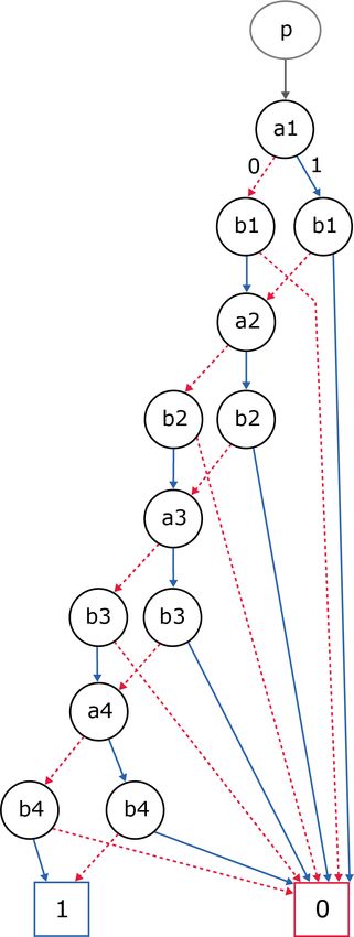
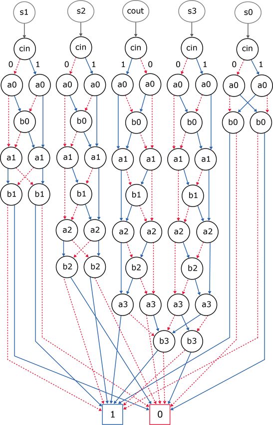
Example 1. The BDD for the FA is shown in Figure 1.

                                                                      An important property of BDDs is that the synthesis op-
                                                                  erations, like AND, OR or composition, can be carried out
                                                                  in polynomial time and space. This can be described by
                                                                  the operator if-then-else (ite) [6, 8]1 . A sketch of the algo-
                                                                  rithm is as follows, where Rh and Rl denote the high- and
                                                                  low-successors, respectively, and e.g. F1i is the cofactor to
                                                                  1 with respect to variable i:

                                                                  ite(F,G,H) {
                                                                    if (terminal case OR
                                                                        (F,G,H) in computed-table) {
                                                                     return result;
                                                                  } else {
              Figure 1. BDD for full adder                          let xi be the top variable of (F,G,H);
                                                                    Rh = ite(F1i,G1i,H1i);
                                                                    Rl = ite(F0i,G0i,H0i);
2.1   Adder Function                                                if (Rh = Rl) return Rh;
   Let a, b and s be three binary numbers of n bits, where          R = find_or_add_unique_table(v,Rl,Rh);
s is the sum of a, b and an incoming carry bit c−1 . The            insert_computed_table(F,G,H,R);
relation between the sum s and the operands a and b can be          return R;
described by the following two equations:                           }
                                                                  }
           ∀n−1
            i=0 ci = ai bi + ai ci−1 + bi ci−1              (1)
                                                                  The ite-operator has a polynomial worst case behavior,
                    ∀n−1        = ai ⊕ bi ⊕ ci−1                  i.e. for graphs F , G and H the result is bounded by
                     i=0 si                                 (2)
                                                                  O(|F | · |G| · |H|). This bound holds under the assump-
The variable ci is called the i-th carry bit. The core cells of   tion of an optimal hashing in O(1). But also in the case of
many adder architectures are the Half Adder (HA) and Full         a worst case behavior of the hashing function, ite remains
Adder (FA) cells realizing a 1-bit addition without or with       polynomial (see [9]).
carry input, respectively. The function table of the HA is
shown in following table:                                         2.3    Symbolic Simulation
                     ai    bi     ha1   ha0
                     0     0       0     0                            To build the BDDs for the output signals of a circuit, the
                     0     1       0     1                        circuit is traversed in a topological order starting from the
                     1     0       0     1                        inputs. For the inputs signals the corresponding BDDs are
                     1     1       1     0                        initially generated. Then, for each gate in the circuit the cor-
It is easy to see that the function ha1 can be realized by an     responding synthesis operation based on ite is carried out.
AND-gate, while ha0 is described by an ⊕-gate, i.e.:              This process is called symbolic simulation in the following.

             ha1 = ai · bi           ha0 = ai ⊕ bi                Example 2. The symbolic simulation for a circuit consist-
                                                                  ing of a single AND gate is shown in Figure 2.
For the FA with inputs ai , bi and ci−1 it holds:
f a1 = ai · bi + ci−1 · (ai + bi )        f a0 = ai ⊕ bi ⊕ ci−1
                                                                  3     Circuit Realization
2.2   Binary Decision Diagrams
   Reduced ordered Binary Decision Diagrams (BDDs) [6,               In this section different realizations for adder circuits are
7] are Directed Acyclic Graphs (DAGs) where a Shannon             briefly reviewed. Only the basic principles are reviewed as
decomposition                                                     far as it is needed for making the paper self-contained. For
                                                                  more details see [10].
               f = xi fxi + xi fxi (1 ≤ i ≤ n)
                                                                     1 Notice that in the following for the discussion and the proofs BDDs

is carried out in each node.                                      without complemented edges are considered.
Figure 2. Symbolic simulation for AND gate
Figure 4. Conditional Sum Adder
3.3 Carry Look Ahead Adder
The Carry Look Ahead Adder (CLA) makes use of a
fast prefix computation in a block Pn (see Figure 5). From
Equation (2) it is obvious that it is sufficient to compute the
carry bits ci for all i. This can be done based on parallel
prefix computation of the generation and propagation prop-
erties for addition. These are described by function g and p,
Figure 3. Ripple Carry Adder respectively:
1. For 0 ≤ i < n: pi,i = ai ⊕ bi , gi,i = ai · bi
3.1 Ripple Carry Adder 2. For i ≤ k < j: pj,i = pk,i · pj,k+1 ,
gj,i = gj,k+1 + (gk,i · pj,k+1 ),
The Ripple Carry Adder (RCA) simply consists of a se-
This means that either a carry bit is generated in the upper
quence on n full adders. The cells are connected via the
part or a carry is generated in the lower part and is propa-
carry chain (see Figure 3).
gated through the higher part. Thus, the carry bits can be
The RCA is very area efficient, since it only requires a computed as (0 ≤ i < n):
linear number of gates. But the RCA is also very slow, since
the delay – measured in the number of gates that has to be ci = gi,0 + pi,0 · c−1
traversed – is also linear in the number of inputs.
The CLA has a logarithmic depth and a size linear in the
number of input variables.
3.2 Conditional Sum Adder
4 Polynomial Verification
The Conditional Sum Adder (CoSA) can be recursively
described. While the lower n/2 bits are computed by a
It is well known that the size of BDDs for the adder func-
CoSA of bit-width n/2, for the higher n/2 bits the result
tion is dependent on the variable ordering. It has also been
is computed by two CoSAs in parallel, where one assumes
proven that the BDD size is linearly bounded (see Section
an incoming carry, while the other does not. Thus, the adder
4.4 in [11]), where exact estimates are given for BDD sizes.
makes use of the fact that the higher bits only depend on the
There, addition without the incoming carry bit has been
incoming carry from the lower half. Both results are pre-
considered. The results can be extended to also consider
computed and the correct result is selected by a multiplexer
the incoming carry bit as it is required for all adder circuits
stage. The computation scheme is shown in Figure 4. For
in the following.
the 1-bit adders, simply full adders can be used.
The CoSA is a fast adder, i.e. it has a depth of O(log(n)). Theorem 1. 1. The sum bit si of an adder has the BDD
The circuit has a gate count of O(n · log(n)). size bounded by 3 · i + 7.4.1 Ripple Carry Adder
For the RCA it is very simple to see that the complete
construction is polynomially bounded. For the HA of the
least significant bit and all FAs the BDD can be locally con-
structed and has only a constant size. Due to the structure of
the RCA each carry output of a cell is connected to the carry
input of the next cell. The substitution of the input variable
can be carried out by the compose algorithm based on ite
and has a polynomial worst-case complexity. Furthermore,
according to Theorem 1 the size of the BDD for the carry
signal for all i is always linear. Thus, the whole construc-
tion process is polynomially bounded, since the composi-
tion only has to be carried out n times.
Figure 5. Carry Look Ahead Adder Theorem 2. The BDD for the RCA can be constructed poly-
nomially.
2. The carry bit ci of an adder has the BDD size bounded
by 3 · i + 6. 4.2 Conditional Sum Adder
Proof. We use the interleaved variable ordering from the The n bit CoSA consists of three CoSAs of bit-size n/2
least to the most significant bits. For the sum bits the results and a multiplexer stage. From Theorem 1 it follows that
from Lemma 4.4.2 in [11] can be generalized, where an up- each of the connecting signals shown in Figure 4 can be
per bound of 3 · i + 5 has been proven for the adder function represented by a BDD of linear size. Only the carry inputs
without an incoming carry bit. For the additional carry bit have to be set to 0 and 1, respectively. The only operation
two more nodes are required, i.e. one for the carry bit itself that has to be carried out is the one corresponding to the
and one for the a0 variable. MUX unit. But this can be described by ite and is polyno-
The same argument holds for the carry bit, but here on mially bounded. Thus, we obtain:
the lowest level one node is saved, since in case of gen-
eration by ai and the incoming carry, bi does not have to Theorem 3. The BDD for the CoSA can be constructed
be tested any more (see Figure 6 for the case of 4 vari- polynomially.
ables).
Remark 3. The results of Theorems 2 and 3 can easily be
It is important to notice that these results were always generalized to further adder types that are based on full
related to the representation size of the output functions, but adders connected together using MUX cells, like √ e.g. the
not for the entire construction process. Carry Select Adder in [12] with a run time of O( n).
Remark 1. In the following, detailed bounds are not pro-
vided, since the goal of this paper is to show that the con- 4.3 Carry Look Ahead Adder
struction process is polynomial.
In the CLA the sum bits are computed by determining the
Thus, it is sufficient to show that each individual step can carry bits first and finally EXOR-ing them with the corre-
be carried out in polynomial time and space. We make use sponding ai and bi inputs according to Equation (2). Thus,
of the following observation: the core circuit computes the carry bits starting based on the
property of generation and propagation, i.e. functions p and
Remark 2. If for each internal signal the size of the BDD
g. The union of propagation intervals is based on Boolean
representation and the number of gates in the circuit is poly-
AND-operations, i.e. larger interval only propagates a carry
nomially bounded in the number of inputs n, the whole cir-
bit, if the left and the right part of the interval do so. For the
cuit can be formally verified in polynomial time due to the
generation part it holds that either the left part (using the
polynomially bounded synthesis operations on BDDs.
higher bits) already propagates or the lower part generates,
This method can be applied to general circuits, but is while the higher part propagates. In both cases, the struc-
used for adders only in the following. For the adder circuits ture consists of AND- and OR-operations only and it can be
from Section 3 the upper bounds hold, that each circuit only seen that the whole structure can be represented by BDDs
has a number of gates polynomial in the number of inputs of polynomial size. More formally, this can be proven as
n. follows:Figure 6. BDD for 4-bit adder function
Lemma 1. 1. Function pj,i has the BDD size bounded by the choice of k does not influence the BDD size and we
3 · (j − i + 1) (j > i). choose k = j − 1 resulting in
2. Function gj,i has the BDD size bounded by 3·(j−i)+2
gj,i = gj,j + (gj−1,i · pj,j ).
(j > i).
Proof. For function pj,i it holds: For each pair of variables al , bl at most 3 nodes can be gen-
erated (see Figure 8 for the case of 4 variables). For the top
pj,i = (aj ⊕ bj )(aj−1 ⊕ bj−1 ) . . . (ai ⊕ bi ) variables even one more node is saved.
The BDD for the EXOR of two variables has three nodes.
Since each variable only appears once, the corresponding
BDDs can simply be connected (see Figure 7 for the case of Based on this observation, the whole BDD for the CLA
4 variables). can be computed based on ite.
Since the BDD is a cannonical representation, in
Theorem 4. The BDD for the CLA can be constructed poly-
gj,i = gj,k+1 + (gk,i · pj,k+1 ) nomially.Figure 7. BDD for p function for 4 variables Figure 8. BDD for g function for 4 variables
Acknowledment
5 Conclusion
Parts of this work have been supported by DFG within
In this paper it has been proven for three different adder the Reinhart Koselleck Project PolyVer: Polynomial Verifi-
architectures that the complete formal verification process cation of Electronic Circuits (DR 287/36-1). Furthermore,
can be carried out polynomially. It was proven that the un- the author likes to thank Alireza Mahzoon for helpful com-
derlying BDDs remain polynomial during the whole con- ments and discussions.
struction process. This was ensured by proving upper
bounds on the BDD sizes for each internal signal. While References
the BDD sizes for the outputs of the adder functions were
known to be polynomially bounded, this is the first time that
[1] R. Drechsler, Advanced Formal Verification. Kluwer
for efficient adder circuits of logarithmic run time a polyno-
Academic Publishers, 2004.
mial proof process could be ensured.
It is focus of future work to identify further classes of [2] ——, Formal System Verification. Springer, 2018.
circuits and functions that can be polynomially verified us-
ing BDDs. Furthermore, alternative proof engines on the [3] R. Bryant, “On the complexity of VLSI implemen-
Boolean level, like SAT or O(K)FDDs, can be considered. tations and graph representations of Boolean func-
Also extension to the word-level, like SMT or WLDDs, will tions with application to integer multiplication,” IEEE
be studied. Trans. on Comp., vol. 40, pp. 205–213, 1991.[4] R. Bryant and Y.-A. Chen, “Verification of arithmetic
functions with binary moment diagrams,” in Design
Automation Conf., 1995, pp. 535–541.
[5] M. Keim, M. Martin, B. Becker, R. Drechsler,
and P. Molitor, “Polynomial formal verification of
multipliers,” in VLSI Test Symp., 1997, pp. 150–155.
[Online]. Available: http://ira.informatik.uni-freiburg.
de/papers/Year_97/KMBDM_97.ps.gz
[6] R. Bryant, “Graph-based algorithms for Boolean func-
tion manipulation,” IEEE Trans. on Comp., vol. 35,
no. 8, pp. 677–691, 1986.
[7] R. Drechsler and B. Becker, Binary Decision Dia-
grams – Theory and Implementation. Kluwer Aca-
demic Publishers, 1998.
[8] K. Brace, R. Rudell, and R. Bryant, “Efficient imple-
mentation of a BDD package,” in Design Automation
Conf., 1990, pp. 40–45.
[9] R. Drechsler and D. Sieling, “Binary decision dia-
grams in theory and practice,” Software Tools for Tech-
nology Transfer, vol. 3, pp. 112–136, 2001.
[10] B. Becker, R. Drechsler, and P. Molitor, Technische In-
formatik - Eine Einführung. Pearson Studium, 2005.
[11] I. Wegener, Branching Programs and Binary Deci-
sion Diagrams - Theory and Application. SIAM
Monographs on Discrete Mathematics and Applica-
tions, 2000.
[12] B. Becker, R. Drechsler, R. Krieger, and S. Reddy, “A
fast optimal robust path-delay-fault testable adder,” in
European Design & Test Conf., 1996, pp. 491–498.You can also read