Proof of Concept for Through Silicon Vias (TSVs) in Application Specific Integrated Circuits (ASICs) for Hard X-ray Imaging Detectors
←
→
Page content transcription
If your browser does not render page correctly, please read the page content below
Proof of Concept for Through Silicon Vias (TSVs) in Application
                                               Specific Integrated Circuits (ASICs) for Hard X-ray Imaging
                                               Detectors

                                               Jaesub Hong*1 , Jonathan Grindlay1 , Branden Allen1 , Daniel P. Violette1 , Hiromasa
                                               Miyasaka2 , Dean Malta3 , Jennifer Ovental3 , David Bordelon3 , Daniel Richter3
                                               1
                                                 Center for Astrophysics | Harvard & Smithsonian, 60 Garden St, Cambridge, MA 02138, USA
                                               2
                                                 California Institute of Technology, Pasadena, CA 91125, USA
arXiv:2103.08749v1 [astro-ph.IM] 15 Mar 2021

                                               3
                                                 Micross Advanced Interconnect Technology, Research Triangle Park, NC 27709, USA

                                               Abstract. Application Specific Integrated Circuits (ASICs) are commonly used to efficiently process the signals from
                                               sensors and detectors in space. Wire bonding is a space qualified technique of making interconnections between ASICs
                                               and their substrate packaging board for power, control and readout of the ASICs. Wire bonding is nearly ubiquitous
                                               in modern space programs, but their exposed wires can be prone to damage during assembly and subject to electric
                                               interference during operations. Additional space around the ASICs needed for wire bonding also impedes efficient
                                               packaging of large arrays of detectors. Here we introduce the Through Silicon Vias (TSV) technology that replaces
                                               wire bonds and eliminates their shortcomings. We have successfully demonstrated the feasibility of implementing
                                               TSVs to existing ASIC wafers (a.k.a. a via-last process) developed for processing the X-ray signals from the X-ray
                                               imaging CdZnTe detectors on the Nuclear Spectroscopic Telescope Array (NuSTAR) Small Explorer telescope mission
                                               that was launched in 2012. While TSVs are common in the semiconductor industry, this is the first (to our knowledge)
                                               successful application for Astrophysics imaging instrumentation. We expect that the TSV technology will simplify
                                               the detector assembly, and thus will enable significant cost and schedule savings in assembly of large area CdZnTe
                                               detectors.

                                               Keywords: ASIC, X-ray, CdZnTe detectors, Wire bond, Through Silicon Vias.

                                               *Jaesub Hong, jhong@cfa.harvard.edu

                                               1 Introduction & Motivation
                                               The discovery and study of the most energetic transient astrophysics phenomena (in order of de-
                                               creasing luminosity) include Gamma-ray bursts of both long and short duration, outbursts from
                                               supermassive black holes (particularly blazars) in galactic nuclei, black hole and neutron star merg-
                                               ers discovered as gravitational wave outbursts, flaring outbursts from black hole and neutron star
                                               X-ray binaries and extreme flares from single M-dwarf stars. These studies are best pursued by
                                               wide-field coded aperture hard X-ray telescopes. The High Resolution Energetic X-ray Imager
                                               (HREXI) is the high resolution imaging 3 - 300 keV X-ray detector designed for optimum readout
                                               of a wide-field coded aperture telescope. Two wide-field, high resolution mission concepts that
                                               employ the HREXI architecture are described in Grindlay et al. (2021).1
                                                   HREXI is composed of close-tiled high spatial resolution CdZnTe (CZT) detectors. The main
                                               heritage of CZT detectors in HREXI comes from the Application Specific Integrated Circuit (ASIC)
                                               used in Nuclear Spectroscopic Telescope Array (NuSTAR)2 and the large CZT detector plane (256
                                               cm2 ) assembled for a series of balloon-borne wide-field hard X-ray imaging telescope experiments
                                               ProtoEXIST1 & 2.3–6 Each 0.3 cm thick CZT crystal in HREXI has an active imaging area of
                                               1.92 × 1.92 cm2 with 32 × 32 0.6 mm pixels that are each conductive-epoxy bonded to the corre-
                                               sponding 32 × 32 pixels on a NuSTAR ASIC (hereafer NuASIC). HREXI groups CZT-NuASICs
                                               into a 2 x 2 close-tiled Detector Crystal Array (DCA) that is read out and individually controlled as

                                                                                                        1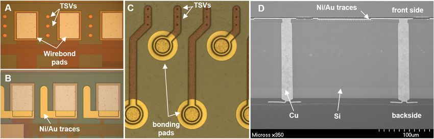
a single unit. But unlike NuSTAR, HREXI allows DCAs themselves to be close-tiled into arbitrarily
large area detector arrays for large area coded aperture imaging with the wide-field and sensitivity
needed for the discovery and study of the energetic transients listed above. What is needed to make
HREXI-based missions feasible is a technology to enable high yield fabrication and assembly of
a large area array of high resolution CZT detectors for multiple wide-field telescopes at relatively
low cost.
    For ProtoEXIST1 & 2 and NuSTAR, the electrical connection between the NuASIC and the
substrate board was made through wire bonding, where each of the 87 wire-bond pads on the
NuASIC is connected to the matching pad on the substrate board underneath through a thin metal
wire. Wire bonding is a space-qualified technique, commonly used for many electronics devices
including detectors and sensors. However, the exposed wires are prone to damage during handling,
and they can complicate the assembly procedure for a large detector array. They can be a source of
electrical noise pickup during operation. Protecting wire bonds through potting or similar methods
can also invite additional electronics noise. In addition, their presence introduces a significant
gap* between CZT detectors, making it difficult to closely tile the detectors into a large array. The
large gaps between the detectors introduce additional background X-ray events and spatial non-
uniformity in the background by allowing X-rays to enter the detectors through the side walls of
CZT crystals (e.g., Figure 7 in Hong et al. 2013).5
    For the last few years, we have been pursuing the Through Silicon Via (TSV) technology to
replace wire bonds and thus eliminate their shortcomings in CZT detector packaging. With TSVs,
the power, control and readout lines in an ASIC can be directly connected to the substrate board
through the full Si layer in the ASIC, enabling flip-chip style bonding. Therefore, TSVs make the
subsequent assembly procedures of detectors robust and simple, and it is projected that they would
enable significant saving in cost and schedule for the assembly of a large array CZT detector plane.
TSVs are implemented at a wafer level on multiple wafers in a single run, whereas wire bonding
requires labor on the individual ASIC dies. CZT detectors can be tiled more tightly with TSVs
by minimizing wasted space in between detectors. In this paper, we present the first successful
implementation of TSVs in the current NuSTAR wafers.
    An increasing number of vendors in the semiconductor industry now routinely utilize TSVs for
‘vertical’ (3-D) packaging of ICs such as memory modules. The typical size of these TSVs is ∼ 5
µm in diameter and 15−50 µm in depth. They are often designed and fabricated in parallel with
the IC circuitry under the careful layout of stacking geometry: i.e., they are implemented through
a ‘via-middle’ process, where TSVs are inserted during foundry runs for the ICs, typically after
transistor fabrication but prior to back end of the line (BEOL) metalization.
    While the via-middle procedure is the most safe approach, redesigning existing ASICs for
TSVs requires considerable resources, often prohibitively expensive under the relatively low fund-
ing of astrophysics instrumentation programs. Instead, we have decided to first demonstrate the
feasibility and benefits of TSVs through a ‘via-last procedure’, where the TSVs are inserted into
the pre-fabricated ASICs on a wafer. The ’via-last’ approach can also be applied to other similar
    * The NuASIC extends about 2.5 mm from the edge pixels on the wire-bond pad side, and the matching pads on

the substrate board requires an additional 2.5 mm gap for safe wire bond installation and protection during assembly.
Thus, with wire bonds, the gap between CZT crystals is about 5 mm on the wire-bond side. With TSVs, this gap can
shrink down to 2.5 mm for the current NuASICs, and the layout of new ASICs in future can be designed to further
minimize this gap with TSVs (see Section 5).

                                                         2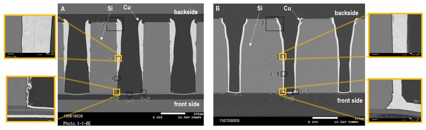
programs that can benefit from removal of wire bonds. One can further divide the via-last pro-
cedure into two different approaches: one inserting blind-TSVs from the back side of the wafer,
and the other inserting through-TSVs from the front side. The successful TSV implementation
demonstrated in this paper has utilized both approaches.
    In this paper, we describe the methodology and performance of the back-side blind-TSV ap-
proach by Vendor #1 in Sections 2 and 3. In Section 4, we describe the concept and advantages of
the front-side through-TSV insertion by Vendor #2 - Micross Advanced Interconnect Technology
(AIT)† , and present the results of the performance measurements from the initial test run. Section 5
presents our vision of future detector assembly and packaging concept using the TSV technology.

2 Implementing Back-side blind-TSVs on NuASIC Wafers
NuASICs are fabricated by ON Semiconductor Corp.‡ on 700 µm thick 8 inch silicon wafers. Each
wafer has 49 NuASIC dies. Figure 1A shows a picture of a mechanical (dummy) version of the
NuSTAR wafer, which was used for the process development of TSV insertion. Each NuASIC
is equipped with 1024 gold stud pixels in a 32 × 32 2-D array, matching the anode pattern of
1024 conductive epoxy dot pixels on a CZT crystal (0.6 mm pixel pitch), to which the NuASIC
bonds directly.5, 7 The 87 wire-bond pads, with 225 µm pitch, that require electric connection
are located along one edge of each NuASIC die (the right hand side in Figure 1B). The silicon
substrate underneath the wirebond pads is free of circuitry, making the NuSTAR wafers suitable for
the via-last procedure.
    Figure 1C illustrates a conceptual cutaway view of the back-side blind-TSVs that connect the
flip-chip style bonding pads on the back side of the ASIC to the aluminum wire-bond pads on
the front side. The basic idea for the back-side TSVs is to implement about 100 µm diameter by
300 µm deep TSVs from the back side of the wafer and touch down on the back of the wire-bond
pads. The NuASIC has three metal layers and the wire-bond pads have all three layers electrically
connected through internal vias to maximize the mechanical stability during the wire-bonding
process. Thus, connecting the TSVs to the back of the metal 3 layer is equivalent to the electric
connection to the wire-bond pad on the top metal layer.
    Figure 2 illustrates the fabrication processes of back-side blind-TSVs by Vendor #1. To achieve
a high yield, the aspect ratio of the TSV height to diameter should be kept less than ∼ 3 to 5. Since
the wire-bond pads are about 150 µm x 120 µm, we settled on TSVs of 100 µm diameter. (A) To
keep the aspect ratio low, we polish NuSTAR wafers down to 300 µm from the 700 µm thickness
of the original NuASIC wafer. (B) The TSV profile is chemically etched out from the back side.
(C) The etched TSVs are passivated with SiO2 to insulate the surrounding Si in the substrate, and a
Ta barrier layer is deposited to prevent Cu diffusion into the Si substrate. (D) Apply directionally-
sensitive Reactive Ion Etch (RIE) to re-open the passivation deposited on the back of the wire-bond
pads. (E) The TSVs are metalized with Cu through multiple stages of sputtering. The back-side
traces and flip-chip pads are plated in parallel. A final passivation is also applied to protect the
TSVs and traces (not shown in the figure).
    Initially the vertical (cylinder shape) profile was adopted for TSVs, but it turns out that with the
vertical profile, the Cu plating process results in excessive accumulation of Cu around the entrance
of the TSVs, leaving little or no Cu plating near the back of the wire-bond pads. After exploring
   †
       http://www.micross.com
   ‡
       www.onsemi.com

                                                   3
a few options to mitigate the issue, a tapered profile (funnel shape) for TSVs was adopted, which
dramatically improved the uniformity in Cu metalization. Figure 4 compares the SEM images of
the TSVs with vertical (left) and tapered (right) profiles. In the former, the Cu (light grey) tends
to get accumulated around the opening of the TSVs while the Cu plating lacks near the back of
the wire-bond pads, resulting in poor conductivity. In contrast, the tapered TSV has the Cu layer
uniformly plated along the entire profile of TSVs, providing good electrical connectivity.

3 Performance of NuSTAR ASIC with back-side blind-TSVs
For diagnostic purpose, each NuASIC is equipped with internal pulser injection capability, which
can trigger the readout sequence in the ASIC. The pulser charges deposited in a group of user-
defined pixels by the internal pulser can be readout just like normal X-ray events. Since the pulser
source is external, the overall spectral resolution of the pulser measurement is subject to stability
of the external source, the build quality of the probe card used for testing ASIC dies, and the ASIC
functionality. We have developed a probe card with a proper probe pin arrangement suitable for
operation from the back side of ASICs through the TSVs. The card circuitry is identical to the one
used for testing the original NuASIC wafers from the front side through the wire-bond pads.
    Figure 3 compares a histogram of internal pulser signals measured through the front-side wire-
bond pads (black) with the same through the back-side TSVs (red) from a NuASIC (Die #47) with
blind-TSVs of vertical profile. The histograms are the sum of the pulser readout from the triggered
pixels, where the first 53 pixels were injected with pulser signals. The spectral resolution of the
internal pulser signals is substantially degraded when measured through TSVs (5.4% FWHM)
relative to the wire-bond pads (3% FWHM). In addition, both measurements, either through TSVs
or wire-bond pads, show noticeable noise events near 0 ADU. Many pixels also exhibit noise
signals above the threshold even without pulser injection: e.g., the measurements through the
TSVs triggered 72 pixels even though only 53 pixels were injected with pulser signals.
    This NuASIC is from the first attempt to implement TSVs from the back side, using the verti-
cal profile. Typically NuASICs (without TSVs) have about 90% yield, but after the TSV insertion,
only about 5 - 6 NuASICs out of 98 NuASICs show some response to external operational com-
mands even when they are probed from the wire-bond pads. Die #47 is the only functioning (albeit
temporary; see below) device out of 98 NuASICs from the 2 wafers that had undergone complete
TSV insertion processes. In fact, all the partially functioning dies also exhibit a high current draw
in the power line, which suggests that the TSV insertion in the first run introduced a kind of short
or current leak somewhere in the system. Die #47 also stopped functioning after a few operations.
We suspect that the current leak permanently damaged the ASIC.
    As shown in the left panel in Figure 4, inspection of the high resolution SEM images of several
TSV profiles revealed uneven etching surface of the TSV profiles especially near the bottom of the
TSVs, suggesting potential electrical shorts between the Cu metal in the TSV and the Si substrate.
We could not pin-point any actual spot of electrical shorts from the SEM images, which is not sur-
prising, given the limited cross-sections one can explore through a few SEM images. Regardless,
to mitigate the issue, the passivation layer of the TSVs were doubled for the 2nd TSV run which
utilized the tapered TSV profiles instead of the vertical profiles.
    Figure 5 compares internal pulser measurements of a pixel on one of the NuASICs through
wire-bond pads before TSV insertion and through TSVs after successful insertion of TSVs with
tapered profiles. The spectrum measured through the TSVs shows an improvement in the spectral

                                                 4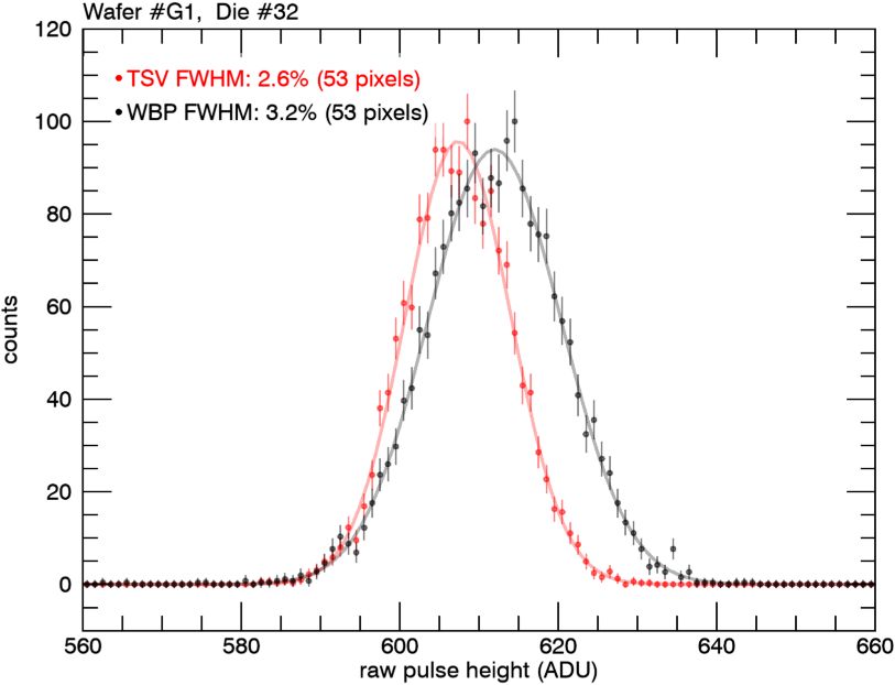
resolution (2.6% FWHM) relative to the measurements conducted through the wire-bond pads
before TSV insertion (3.1% FWHM). These ASICs with tapered profile TSVs show no excessive
noise events and their performance is stable over time unlike Die #47 in the earlier run. Despite
the fact that the signal path length is slightly longer by as much as ∼ 1 mm when probed through
the TSVs compared to the wire-bond pads, the improved spectral resolution in the measurements
through TSVs is encouraging. In a completed detector assembly, the electrical paths through wire
bonds are longer and more exposed than those through TSVs, and thus the system with TSVs is
expected to be less susceptible to external noises. Note that pulser measurements of NuASICs
depend on the stability of the external pulser source and the build quality of the probe cards as well
as the ASIC performance. Nonetheless, the results indicate that the proper TSV insertion process
does not degrade the ASIC performance.
The left panel in Figure 6 compares the pulser measurements of the NuASICs where measure-
ments through both wire-bond pads and TSVs are available for the same ASIC. Each data point is
labeled by wafer and ASIC die IDs. Note the measurements through wire-bond pads for ASICs in
Wafers #3 and #4 were conducted before TSV insertion. TSVs in Wafer #2 have vertical profiles,
and ones in Wafers #3 and #4 have tapered profiles. All the NuASICs with tapered profile TSVs
show improvements in the pulser resolution when measured through TSVs compared to wire-bond
pads. The right panel shows all the measurements we have conducted for ASICs in Wafers #3
and #4, where the measurements through TSVs statistically outperform the measurements through
wire-bond pads in spectral resolution, indicating a successful demonstration of the proof of con-
cept for the via-last process for TSVs. The overall yield of the successful TSV implementation in
Wafers #3 and #4 are about 70% after accounting for the overall non-TSV NuASIC yield (90%).
Despite the relatively high yield in successful TSV implementation, we were not successful in
assembling fully functioning CZT detectors from these TSV NuASICs. One of the main causes
was excessive plating of back-side traces and bonding pads in part due to inexperience in trace
plating of Vendor #1. As a result, many traces were shorted to each other, making a large number
of dies unusable. Over-plating also introduced unnecessary stress in the wafers, which resulted
in large cracks in the wafers during the debonding process of the carrier layer. The carrier layer
is temporarily attached to protect thin wafers during the TSV implementation. The cracks further
reduced the number of workable dies. Only 17 out of 98 NuASICs from the two wafers were
properly plated for the traces and pads on the back side. In the case of Wafer #4, the carrier layer
debonding was abandoned due to the risk of cracking, which renders all the ASICs unusable for
subsequent detector assembly since the carrier layer blocks access to the pixel pads on the front
side.
Debonding of the carrier layer from Wafer #3 revealed another weakness in the TSV imple-
mentation from the back side. Since TSVs touch down on the back of the wire-bond pads and the
majority volume of the TSVs is not filled, the structural integrity of wire-bond pads is compromised
after TSV insertion. As a result, the debonding process often delaminates parts or all of some wire-
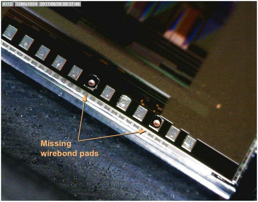
bond pads (Figure 7), which makes the ASIC unusable either through TSVs or wire bonds. Only
one (Wafer #3 Die #47) out of the 11 functioning TSV NuASICs survived the debonding process
without loss of wire-bond pads and functions properly after the assembly with the substrate board.
Another weakness of the back-side TSV implementation is in the nature of the blind vias. It
is difficult to reach and process the region where TSVs touch down on the wire-bond pads. The
touch-down region also tends to develop unwanted chemical reactions and leave chemical residue
while undergoing the multiple processes of etching and plating. This residue is often difficult to
5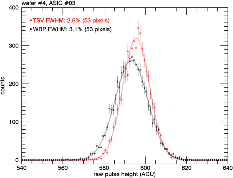
clean. As a result, this approach requires relatively expensive wafer processing tools, which small
vendors may not have access to. In contrast, relatively large wafer processing vendors do have
these necessary tools, but they often do not show interest in small volume development projects
like ours. Unfortunately, Vendor #1, which performed the runs described in the above sections,
stopped offering TSV services needed for our development after a recent corporate restructuring,
and we had to search for other vendors. We did regroup with a new vendor that retained some of
key members from Vendor #1, who had worked on our TSV development effort. The subsequent
attempt with the new vendor to implement back-side blind-TSVs, however, was unsuccessful due
to lack of necessary tools, despite a few novel ideas to address the challenges.

4 Front-side through-TSVs and their performance
With the successful proof of the TSV concept, we searched for a new approach that enables high
yield in detector assembly with relatively easily accessible tools. A promising approach is the
implementation of true through-Silicon vias from the front side of wafers (instead of back-side
blind-TSVs). This approach resolves the difficulties in the previous runs with TSV etching, met-
allization, and interconnection to the ASIC bond pads. We have finished the initial test run of
implementing front-side TSVs on 3 NuASIC Wafers with our current industry partner, Micross
Advanced Inter-connect Technology (AIT).
    Figure 8 illustrates the fabrication processes of the front-side through-TSVs. (A) The front side
of the wafer is passivated and the (vertical) profiles of TSVs are etched out next to wire-bond pads.
(B) After properly passivating the TSVs with SiO2 and depositing the Cu-barrier layers (TiN) to
prevent Cu diffusion into the Si wafer, the TSVs are Cu-filled along with the front surface. (C) The
front-side Cu deposit is polished off so that the wafer surface is planarized with SiO2 remaining
over the Al pad, and then, both wire-bond pads and pixel pads are exposed through etching. (D)
The Ni/Au traces connecting TSVs to wire-bond pads are deposited on the front side, and then the
back side is polished and etched to expose the TSVs. (E) Passivate the back side and deposit the
proper metal traces and solder bump pads on the back side for flip-chip bond.
    This approach does not disturb the Si substrate below the wire-bond pads on the front side of
the original NuASIC, so there is no risk of weakening or losing any wire-bond pads in the process.
The Cu metal is deposited inside the TSVs after the TSVs profiles are etched blind (C), but the
blind end of the TSVs are revealed again through dry etch after polishing, so there is no concern of
developing any complex chemical residues that require careful cleaning and monitoring. This in
turn enables use of relatively small vias (20 µm diameter). These small TSVs are fully Cu-filled,
improving the mechanical integrity of each die.
    Our relatively small TSVs allow 3 TSV insertions for each wire-bond pad, improving the yield
in conductivity. Figure 9 shows a small region around a few wire-bond pads during TSV imple-
mentation: (A) the front side after Cu-filling TSVs (3 TSVs per wire-bond pad), (B) the front side
after Ni/Au trace layout connecting TSVs to an edge of each wire-bond pad, (C) the bottom side
showing the TSVs, flip-chip style pads, and connecting traces and (D) an SEM image of the TSV
cross section. As mentioned, we inserted 3 TSVs for each wire-bond pad in between each wire-
bond pad. We laid out the connecting traces between TSVs and the wire-bond pads. The majority
of the original Al wire-bond pads are exposed so that in principle wire bonding can be applied
to these ASICs if needed. The pads for flip-chip style bonding on the back side are now made
in a circular shape (instead of the original rectangular shape; see Figure 1C) in order to improve

                                                 6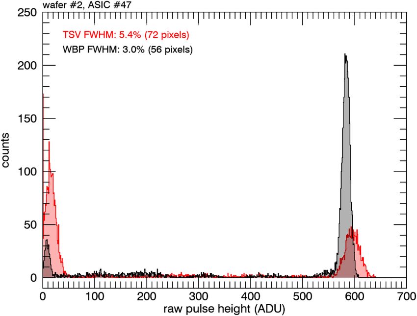
the uniformity in the spherical solder ball attachment and spread, which in turn improves bonding
quality. The pads are coated with Ni and Au to avoid oxidization.
    Figure 10 shows the pulser performance measured through the TSVs (red) in comparison with
the same through the wire-bond pads (black). The measurements through the wire-bond pads were
done before the TSV implementation. Some of the measurements through the TSVs were done
using the ASIC Test Setup (ATS) developed at Harvard.8, 9 The ATS is designed to enable rapid
test and screening of TSV ASICs through quick and easy alignment of pogo-pins and the back-
side pads or solder bumps on the pads of the ASIC. The distribution is a sum of the pulser data
from the first 53 pixels of Wafer #G1 and Die #32. This demonstrates the successful operations in
the ASICs with front-side through-TSVs. The overall spectral resolution improved again with the
TSVs relative to the operation through wire-bond pads.
    Among 15 font-side TSV NuASICs that were tested so far, 4 NuASICs show a good pulser
performance (similar to Figure 10) in the initial pulser runs, showing about 30% of yield. While
this yield appears to be small relative to the earlier run, we believe that the yield is nearly 100% in
terms of the conductivity of TSVs. In this initial run for the front-side TSVs, a set of daisy chained
TSVs are inserted to each ASIC die for diagnostic purpose, where the electrical conductivity and
isolation of TSVs can be tested.10 According to the conductivity test of the daisy chain, the average
resistivity of TSVs is less than 1 Ω with practically 100% yield. The cause of the relatively low
yield in the overall functionality is suspected to be the insufficient isolation or insulation of the
TSVs.
    In fact, all of the tested ASICs draw the increasingly higher current in the power line over time
during the pulser tests, and eventually became unresponsive after about 10 minutes of operation.
Subsequent power cycle would start the ASIC at a relatively higher current draw state even after
a few days of non-operation, and the ASICs become unresponsive within a minute. This result
is consistent with the isolation tests of the daisy chain TSVs, where the current leak between
relatively nearby TSVs (electrically unconnected) was observed to increase over time.10
    While we are investigating the root cause of this current instability, the observed symptoms
resemble what we had experienced with the very first run of the back-side blind-TSV implemen-
tation, where all the dies draw high currents in the power line and their functionality was unstable.
The most likely cause is the insufficient thickness for the SiO2 insulation and/or Cu barrier layer
surrounding each TSV as well as between the Cu traces and underlying Si wafer. In fact, the first
run of the back-side blind-TSV implementation had issues in both TSV conductivity and isolation,
which resulted in a poor spectral resolution (Figure 3) and a low yield (∼ 1%). It is clear that the
front-side through-TSVs in this first trial run have good conductivity but poor insulation according
to both the pulser and daisy chain tests. We plan to increase the thickness of SiO2 insulation and
Cu barrier layers, which had resolved the similar issue for the back-side blind-TSVs. As we learn
more about the cause of the high current draw and instability, we will further revise the processes,
which will be applied in the next run for the front-side through-TSV implementation. Given the
good conductivity of the front-side TSVs, we expect that the overall yield for successful NuASICs
with front-side TSVs will exceed the 70% yield in the back-side TSV NuASICs of the 2nd-run
once we resolve the TSV isolation issue.

                                                  7
5 Summary and Detector Assembly with TSVs
We presented the first successful proof of concept for TSVs to replace wire bonds for readout
and control of ASICs bonded to CZT imaging detectors. We used two approaches. While both
are viable, the approach using front-side through-TSVs resolves major weaknesses in the other
approach using back-side blind-TSVs, enabling an easier and cleaner path for both TSV insertion
and final detector assembly.
With the TSV NuASICs, we can envision true 3-D stacking of the backend electronics for CZT
detector assembly in future as illustrated in Figure 11. The current design of our CZT detector
assembly employs a set of Field Programmable Gate Arrays (FPGAs) and complex programmable
logic devices (CPLDs) to control and readout the NuASICs. These logic devices are mounted in the
substrate board where the NuASICs are mounted and connected through wire bonds (Figure 11A).
With TSVs, assembly between the CZT crystal, the NuASIC and the substrate board is achieved
essentially through a series of flip-chip style bonding (Figure 11B). Once the operational code
of the logic devices are well defined and frozen, the front end of the FPGAs can be turned into
another signal-processing ASIC, which can be directly 3-D stacked underneath the ASIC using
TSVs (Figure 11C). The design of NuASIC itself can be further optimized to minimize the gap
between the CZT crystals. One can go a step further, the layout of both the NuASIC and the signal
processing ASIC can be designed with TSVs in mind. The TSV technology enables easy, robust
and low cost assembly and packaging concept to a wide range of detector and sensor systems.
6 Acknowledgement
This work was supported by NASA APRA grant NNX17AE62G.
References
1 J. Grindlay, et al., “4pi X-ray Imaging Observatory (4piXIO): Transformative Time Domain
Astrophysics,” in preparation (2021).
2 F. A. Harrison, W. W. Craig, F. E. Christensen, et al., “The Nuclear Spectroscopic Telescope
Array (NuSTAR) High-energy X-Ray Mission,” The Astrophysical Journal 770, 103 (2013).
3 J. Hong, B. Allen, J. Grindlay, et al., “Building large area CZT imaging detectors for a wide-
field hard X-ray telescope—ProtoEXIST1,” Nuclear Instruments and Methods in Physics
Research A 605, 364–373 (2009).
4 B. Allen, J. Hong, J. Grindlay, et al., “Development of the ProtoEXIST2 advanced CZT
detector plane,” Proc. IEEE Nuclear Science Symp. and Medical Imaging Conf. , 4470–4480
(2011).
5 J. Hong, B. Allen, J. Grindlay, et al., “Tiled Array of Pixelated CZT Imaging Detectors
for ProtoEXIST2 and MIRAX-HXI,” IEEE Transactions on Nuclear Science 60, 4610–4617
(2013).
6 J. Hong, B. Allen, J. Grindlay, et al., “Imaging Analysis of the Hard X-Ray Telescope Pro-
toEXIST2 and New Techniques for High-resolution Coded-aperture Telescopes,” The Astro-
nomical Journal 153, 11 (2017).
7 F. A. Harrison, W. R. Cook, H. Miyasaka, et al., Semiconductor Radiation Detection Systems,
CRC Press, Boca Raton, FL (2010).
88 D. Violette, B. Allen, J. S. Hong, et al., “Efficient validation testing of Through-Silicon-Via
(TSV) ASICs for CZT x-ray detectors,” in Hard X-Ray, Gamma-Ray, and Neutron Detector
Physics XX, Society of Photo-Optical Instrumentation Engineers (SPIE) Conference Series
10762, 107620S (2018).
9 D. P. Violette, et al., “Testing Station for Fast Screening of Through Silicon Via (TSV) ASICs
for Hard X-ray Detectors,” in preparation (2020).
10 J. Ovental, D. Malta, D. Bordelon, et al., “TSV-last Integration to Replace ASIC Wire Bonds
in the Assembly of X-ray Detector Arrays,” in Proc. of 2021 IEEE 71st Electronic Compo-
nents and Technology Conference, IEEE Press, accepted for publication (2021).
Biographies
Jaesub Hong is a Research Associate at Harvard University. He has nearly 20 years of experi-
ence in development of X-ray telescopes for high energy astrophysics and planetary science. His
current focus is the development of advanced hard X-ray detectors for next generation wide-field
hard X-ray telescopes for time domain astrophysics and the miniature lightweight X-ray optics
for planetary science. He received a Ph.D. degree in Physics from Columbia University. He has
(co)authored over 40 publications.
Jonathan (Josh) Grindlay is the Robert Treat Paine Professor of Astronomy at Harvard. He
received his BA in Physics from Dartmouth (1966) and PhD in Astrophysics from Harvard (1971).
He joined the Faculty in 1976 and Chaired the Department in 1985-91 and 2001-03. His primary
interest is black hole time variability, accretion physics, accreting black hole (both stellar and
supermassive) populations and formation as measured with wide-field coded aperture imaging X-
ray telescopes (ultimately full-sky) and optical/IR imaging/spectroscopy. He has over 434 refereed
Journal papers.
Branden Allen received his Ph.D. degree in physics from U.C. Irvine in 2007 and is currently
a Research Associate at Harvard University with over 20 years of experience in the development,
deployment and operation of ground- and space-based telescopes for high-energy X/γ-ray astron-
omy and planetary science. His current research is focused on the development and deployment
of next generation detector systems and telescopes to probe high energy astrophysical phenomena
and for future planetary exploration.
Daniel Violette is a graduate student at Harvard University working with the High-Resolution
Energetic X-ray Imager (HREXI) team, with interests in high-energy time domain astrophysics
and instrumentation. Daniel is supported by the Future Investigators in NASA Earth and Space
Science and Technology (FINESST) Fellowship to further develop HREXI detector sensitivity at
low energy thresholds.
Hiromasa Miyasaka is a staff scientist at California Institute of Technology. He received a
Ph.D. in Physics (2000) from Saitama University in Japan. He has over 20 years of experience
in development of particles and X-ray detectors for the cosmic ray and high-energy astrophysics.
Since 2006, his work has focused on CdZnTe and CdTe detectors and readout ASIC development.
He is one of the primary detector scientists for the NuSTAR mission.
Dean Malta is a Program Manager at Micross AIT. His work has spanned nearly 30 years
in microelectronics packaging, fiber optic components, and wide bandgap semiconductor devices.
9His current focus is the development of 3D and heterogeneous integration technologies for ad-
vanced electronic modules and photonic sensors. Dean received a B.S. in Electrical Engineer-
ing from Wilkes University. He is a Senior Member of IEEE, holds 6 U.S. patents, and has
(co)authored over 75 publications.
Jennifer Ovental is a Development Engineer at Micross AIT. Her primary focus is on 3D
and Heterogeneous Integration, particularly in the areas of through-silicon via technology and mi-
crobump processes for ultra-fine pitch chip bonding. She received her BS in Chemical Engineering
(2012) from Lafayette College and her Ph.D. in Chemical Engineering (2018) from North Carolina
State University. Her graduate research and published work was predominately focused on atomic
layer deposition.
David Bordelon is a Development Engineer in Advanced Packaging and 3D Integration for
government and commercial programs with Micross AIT. He received his BS in Applied Science
(1994) and Ph.D. (2009) in Materials Science from UNC-Chapel Hill. His published articles in-
clude Ph.D. work on biomedical applications of carbon nanotube field emission and post-doctoral
research in nanomaterial-mediated cancer thermotherapy at Johns Hopkins. He gained extensive
microfabrication expertise during 10+ years of prior Optical-MEMS & Microsystems develop-
ment.
Daniel Richter is a Development Engineer at Micross AIT and is responsible for the develop-
ment and implementation of advanced assembly and semiconductor packaging technology. He has
extensive design experience and takes a lead role in photomask layout. He holds multiple patents
relating to semiconductor packaging technology. Daniel received a B.S. degree in Material Science
Engineering and M.S. degree in Nanoengineering from North Carolina State University.
Tables
N/A
Figures
Fig 1 (A) A mechanical wafer with 49 ASIC dies was used to develop the TSV process. (B) Each NuSTAR ASIC has
87 wire-bond pads on one edge for power, control and readout. The inset shows a closeup view of 6 wire-bond pads
with 225 µm pitch. (C) Cutaway view of back-side blind-TSV concept for NuSTAR ASIC (NuASIC). TSVs connect
the flip-chip bonding pads on the back side of the ASIC to the back of the wire-bond pads on the front side of the
NuASIC.
10Fig 2 Back-side blind-TSV fabrication processes by Vendor #1: (A) Back-side polishing and passivation. (B) Blind
TSV etching. (C) TSV passivation and Cu-barrier layer installation. (D) Exposing the bottom passivation of TSVs
through directionally sensitive etching. (E) Electroplating Cu on TSVs to make electric connection.
Fig 3 Pulser spectra comparison between wire-bond pads and blind-TSVs with vertical profiles from Wafer #2 Die
#47 by Vendor #1. The measurements through the TSVs degrade the spectral resolution, and both measurements show
additional noise events near 0 ADU.
11Fig 4 SEM images of back-side blind-TSV profiles by Vendor #1: (A) Vertical profile with cylinder shape. (B) Tapered
profile with funnel shape.
Fig 5 Pulser spectra comparison between wire-bond pads and blind-TSVs with tapered profiles from Wafer #3 Die #3
by Vendor #1. The measurements through the TSVs show an improvement in the spectral resolution, compared to the
measurements through the wire-bond pads.
Fig 6 Spectral resolution comparison between wire-bond pads and blind-TSVs by Vendor #1. (Left) the ASIC dies
with both measurements available. (Right) Resolution distribution of all the measurements for Wafers #3 and #4.
12Fig 7 Loss of wire-bond pads during carrier layer debonding for blind-TSV implementation by Vendor #1. Among
12 wire-bond pads visible in this view, two pads were delaminated during the debonding process of the carrier layer,
which revealed the TSVs underneath.
Fig 8 Front-side through-TSV fabrication processes by Vendor #2 (Micross AIT): (A) front-side passivation and TSV
etching. (B) TSV and front-side metalization. (C) Exposing wire-bond pads through chemical-mechanical polishing,
surface planarizing and etching. (D) Deposition of traces connecting TSVs and wire-bond pads, and exposing TSVs
from the back side through polishing followed by etching. (E) Trace and pad deposition on the back side along with
proper passivation.
13Fig 9 Progress of the through-TSV implementation by Vendor #2 (Micross AIT): (A) the front side after TSV Cu-
filling and polishing, showing TSVs next to wire-bond pads (3 TSVs per wire-bond pad were employed), (B) the
front side with traces connecting TSVs to wire-bond pads, (C) the back side showing TSVs, solder bump pads and
connecting traces, and (D) an SEM image of the TSVs.
Fig 10 Pulser performance of a NuASIC with front-side TSVs by Vendor #2 (Micross AIT): measurements through
TSVs (red) in comparison with the same through wire-bond pads (black).
Fig 11 (A) CZT and ASIC assembly using wire bonds. (B) The same with TSVs. (C) CZT, ASIC and backend ASIC
assembly using 3-D stacking.
14You can also read