Roadmap on emerging hardware and technology for machine learning - IOPscience
←
→
Page content transcription
If your browser does not render page correctly, please read the page content below
Nanotechnology

ROADMAP • OPEN ACCESS

Roadmap on emerging hardware and technology for machine learning
To cite this article: Karl Berggren et al 2020 Nanotechnology 32 012002

View the article online for updates and enhancements.

                               This content was downloaded from IP address 46.4.80.155 on 22/10/2020 at 06:21
Nanotechnology
Nanotechnology 32 (2020) 012002 (45pp) https://doi.org/10.1088/1361-6528/aba70f
Roadmap
Roadmap on emerging hardware and
technology for machine learning
Karl Berggren1,36, Qiangfei Xia2,36, Konstantin K Likharev3, Dmitri B Strukov4,
Hao Jiang5, Thomas Mikolajick6, Damien Querlioz7, Martin Salinga8,
John R Erickson9, Shuang Pi10, Feng Xiong9, Peng Lin1, Can Li11, Yu Chen12,
Shisheng Xiong12, Brian D Hoskins13, Matthew W Daniels13, Advait Madhavan13,14,
James A Liddle13, Jabez J McClelland13, Yuchao Yang15, Jennifer Rupp16,17,
Stephen S Nonnenmann18, Kwang-Ting Cheng19, Nanbo Gong20,
Miguel Angel Lastras-Montaño21, A Alec Talin22, Alberto Salleo23, Bhavin J Shastri24,
Thomas Ferreira de Lima25, Paul Prucnal25, Alexander N Tait26, Yichen Shen27,
Huaiyu Meng27, Charles Roques-Carmes1, Zengguang Cheng28,29, Harish Bhaskaran28,
Deep Jariwala30, Han Wang31, Jeffrey M Shainline26, Kenneth Segall32,
J Joshua Yang2,37, Kaushik Roy33, Suman Datta34 and Arijit Raychowdhury35
1
Research Laboratory of Electronics, Massachusetts Institute of Technology, Cambridge, MA 02139,
United States of America
2
Department of Electrical and Computer Engineering, University of Massachusetts, Amherst, MA,
United States of America
3
Stony Brook University, Stony Brook, NY 11794, Unites States
4
Department of Electrical and Computer Engineering, University of California at Santa Barbara,
Santa Barbara, CA 93106, United States of America
5
School of Engineering & Applied Science Yale University, CT, United States of America
6
NaMLab gGmbH and TU Dresden, Germany
7
Université Paris-Saclay, CNRS, France
8
Institut für Materialphysik, Westfälische Wilhelms-Universität Münster, Germany
9
Department of Electrical and Computer Engineering, University of Pittsburgh, Pittsburgh, PA 15261,
United States of America
10
Lam Research, Fremont, CA, United States of America
11
Department of Electrical and Electronic Engineering, The University of Hong Kong, Hong Kong SAR,
China
12
School of information science and technology, Fudan University, Shanghai, People’s Republic of China
13
Physical Measurements Laboratory, National Institute of Standards and Technology, Gaithersburg,
MD 20899, United States of America
14
Institute for Research in Electronics and Applied Physics, University of Maryland, College Park, MD,
United States of America
15
School of Electronics Engineering and Computer Science, Peking University, Beijing,
People’s Republic of China
16
Department of Materials Science and Engineering and Department of Electrical
Engineering & Computer Science, Massachusetts Institute of Technology, Cambridge, MA 02139,
United States of America
17
Electrochemical Materials, ETHZ Department of Materials, Hönggerbergring 64, Zürich 8093,
Switzerland
Original content from this work may be used under the
terms of the Creative Commons Attribution 4.0 licence. Any
further distribution of this work must maintain attribution to the author(s) and
the title of the work, journal citation and DOI.
1361-6528/20/012002+45$33.00 1 © 2020 IOP Publishing Ltd Printed in the UK
Nanotechnology 32 (2020) 012002                                                                            Roadmap

18
   Department of Mechanical & Industrial Engineering, University of Massachusetts-Amherst, MA,
United States of America
19
   School of Engineering, Hong Kong University of Science and Technology, Clear Water Bay, Kowloon,
Hong Kong, People’s Republic of China
20
   IBM T J Watson Research Center, Yorktown Heights, NY 10598, United States of America
21
   Instituto de Investigación en Comunicación Óptica, Facultad de Ciencias, Universidad Autónoma de
San Luis Potosí, México
22
   Sandia National Laboratories, Livermore, CA 94551, United States of America
23
   Department of Materials Science and Engineering, Stanford University, Stanford, California, United
States of America
24
   Department of Physics, Engineering Physics & Astronomy, Queen’s University, Kingston ON KL7
3N6, Canada
25
   Department of Electrical Engineering, Princeton University, Princeton, NJ 08544, United States of
America
26
   Physical Measurement Laboratory, National Institute of Standards and Technology (NIST), Boulder,
CO 80305, United States of America
27
   Lightelligence, 268 Summer Street, Boston, MA 02210, United States of America
28
   Department of Materials, University of Oxford, Oxford OX1 3PH, United Kingdom
29
   State Key Laboratory of ASIC and System, School of Microelectronics, Fudan University, Shanghai
200433, People’s Republic of China
30
   Department of Electrical and Systems Engineering, University of Pennsylvania, Philadelphia PA
19104, United States of America
31
   University of Southern California, Los Angeles, CA 90089, United States of America
32
   Department of Physics and Astronomy, Colgate University, NY 13346, United States of America
33
   School of Electrical and Computer Engineering, Purdue University, West Lafayette, IN 47907, United
States of America
34
   University of Notre Dame, Notre Dame, IN 46556, United States of America
35
   Georgia Institute of Technology, Atlanta, GA 30332, United States of America

E-mail: berggren@mit.edu and qxia@umass.edu

Received 20 November 2019, revised 24 February 2020
Accepted for publication 17 July 2020
Published 19 October 2020

Abstract
Recent progress in artificial intelligence is largely attributed to the rapid development of
machine learning, especially in the algorithm and neural network models. However, it is the
performance of the hardware, in particular the energy efficiency of a computing system that sets
the fundamental limit of the capability of machine learning. Data-centric computing requires a
revolution in hardware systems, since traditional digital computers based on transistors and the
von Neumann architecture were not purposely designed for neuromorphic computing. A
hardware platform based on emerging devices and new architecture is the hope for future
computing with dramatically improved throughput and energy efficiency. Building such a
system, nevertheless, faces a number of challenges, ranging from materials selection, device
optimization, circuit fabrication and system integration, to name a few. The aim of this
Roadmap is to present a snapshot of emerging hardware technologies that are potentially
beneficial for machine learning, providing the Nanotechnology readers with a perspective of
challenges and opportunities in this burgeoning field.
Keywords: artificial intelligence, machine learning, neural network models, neuromorphic
computing, hardware technologies
(Some figures may appear in colour only in the online journal)

36
     Author to whom any correspondence should be addressed.
37
     Present address: University of Southern California, Los Angeles, CA 90089, United States of America

                                                                             2
Nanotechnology 32 (2020) 012002                                        Roadmap

Contents

 1. Floating gate memory-based hardware                                     5
 2. Materials consideration for emerging devices                            8
 3. Scaling of emerging hardware and technology for machine learning       11
 4. Heterogeneous integration of emerging device arrays                    13
 5. The processing strategies for memristor crossbar fabrication           15
 6. Defectivity and its impact on hardware neural networks                 18
 7. In situ and in operando metrology and characterization                 21
 8. Variability in emerging memory devices and solutions                   24
 9. The organic redox transistor for neuromorphic computing                27
10. Light-based neuromorphic computing                                     29
11. 2D materials-based emerging memristive devices                         33
12. Superconducting hardware for neuromorphic computing                    36
13. Towards spiking neural networks                                        39
References                                                                 41

                                                           3
Nanotechnology 32 (2020) 012002                                                                                                     Roadmap

Introduction                                                               system for scalable algorithms such as backpropagation. For
                                                                           devices with intrinsic dynamic behavior similar to biological
It is believed that hardware is on the critical path for the future        synapse and neurons, they may be promising building blocks
of artificial intelligence in the big data era [1]. State-of-the-art       for spiking neural networks (SNNs) that takes advantage of the
hardware for machine learning such as the central processing               timing in electric pulses for computing.
unit, graphics processing unit (GPU) and tensor processing                     Extensive simulation has shown that neural networks built
unit (TPU) are built upon complementary metal oxide semi-                  with emerging non-volatile memories will bring orders of
conductor (CMOS) transistors. Although superior computing                  magnitude higher speed-energy efficiencies [3]. However,
capability has been demonstrated with such hardware, the end               experimental demonstration of large systems that can solve
of transistor scaling and the separation of logic and memory               real-world problems has had limited success to date in part
units in the von Neumann architecture limit performance, in                because of the lack of ideal devices that can efficiently imple-
particular energy efficiency, for data-centric tasks. Inspired             ment the machine learning algorithms or faithfully emulate the
by the extremely low power consumption of the human brain,                 essential properties of synapses and neurons. In addition, the
neuromorphic hardware has been an intensive research topic,                heterogeneous integration of the devices into massively paral-
such as those based on emerging solid state devices.                       lel networks is a major technical obstacle as well.
    Emerging non-volatile devices can store information                        In the present Roadmap article, we pick up several top-
without dissipating power. When organized into a computing                 ics on the emerging neuromorphic hardware and technology
system, they can implement the so-called ‘in-memory comput-                with machine learning applications that we think are partic-
ing’ (IMC) paradigm, in which computation takes place where                ularly appealing to the readers of Nanotechnology, a com-
the data is stored. IMC avoids the time and energy spent on                munity that is more interested in device and technology rather
data shuttling between memory and logic units in a traditional             than machine learning algorithm and neural network archi-
digital computer, especially suitable for tasks in which data              tecture. The Roadmap starts with FLASH-based hardware
needed to be computed are naturally collocated in the physical             that uses non-volatile transistors and targets inference sys-
memory. Taking advantage of physical laws, such as Ohm’s                   tems. We believe this is a good segue from CMOS to emer-
law for multiplication and Kirchhoff’s current law for summa-              ging devices. Several resistance switching phenomena-based
tion, IMC with a large-scale emerging device offers massive                devices including the phase change, memristor, magnetores-
parallelism as well. Furthermore, the physical computing is                istance and ferroelectric devices are the subject of the next
analog in nature and the hardware could interface with ana-                few sections, including the materials selection, electrical prop-
log data acquired directly from sensor arrays, reducing the                erty optimization, device fabrication and circuit integration,
energy overhead from analog/digital conversions. Depending                 and metrology control, etc. In addition, new materials (such
on the properties of the device, such hardware is suitable for             as 2D materials and organic materials) and technologies (for
three types of applications [2]. Devices with excellent stabil-            example, self-assembly) are also covered. Finally, novel con-
ity can be used to build an inference system where the synaptic            cepts, such as using photons, quantum phenomenon, super-
weights have already been trained somewhere else. With high                conductors and the timing of electrical spikes for computing
enough endurance, they may be incorporated into a training                 are introduced.

                                                                       4
Nanotechnology 32 (2020) 012002                                                                                                Roadmap

1. Floating gate memory-based hardware                                 and 20 nJ, i.e. at least three orders of magnitude better
                                                                       than those obtained with the 28 nm digital TrueNorth chip
Konstantin K Likharev1 and Dmitri B Strukov2                           used for the same task, with a similar fidelity. Preliminary
1                                                                      experimental results for the chip-to-chip statistics, long-term
  Stony Brook University, Stony Brook, NY 11794, United
                                                                       drift, and temperature sensitivity of the network are also
States of America
2                                                                      encouraging [9].
  UC Santa Barbara, Santa Barbara, CA 93106, United States
of America
                                                                       Current and future challenges
Status
                                                                       There are at least two major current challenges to this
The present-day revolution in deep learning, triggered by the          approach. First, the implementation of practically use-
use of high-performance hardware, in turn has stimulated               ful, general-purpose, reconfigurable neuromorphic processors
the development of even more powerful digital systems, spe-            have to be employed. Recent architectures addressing this
cific for machine learning tasks. However, the use of digital          challenge (e.g. the aCortex [5]) are typically based on rectan-
operations for the implementation of neuromorphic networks,            gular arrays of analogue FG crossbars performing the VMM
with their high redundancy and noise/variability tolerance, is         function, connected via digital interfaces to the main memory
inherently unnatural. Indeed, the performance of such net-             used for storing input, output, and intermediate data. Such
works may be dramatically improved using analog and mixed-             architecture allows for storage of synaptic weights locally,
signal integrated circuits. In this approach, the key operation—       thus avoiding performance-penalizing communications with
vector-by-matrix multiplication (VMM)—is implemented on                the off-chip memory. Not surprisingly, the first simulations
the physical level in a crossbar circuit, using the fundamental        of the aCortex, based on experimental data from prototype
Ohm and Kirchhoff laws (figure 1(a)) [4].                              VMM circuits, have already shown significant advantages in
    The main difference between numerous recently demon-               energy efficiency over its digital counterparts (figure 2(d)),
strated circuits of this type is the choice of crosspoint              which would be even more dramatic with a proper account
devices with adjustable conductance G—essentially analogue             of the off-chip data transfer overhead in digital systems.
non-volatile memory cells, storing the pre-recorded synaptic           (Furthermore, simulations have shown that similarly super-
weights w ∝ G. Much recent effort has been devoted to                  ior energy efficiency may also be reached in mixed-signal
using, in this role, memristors and other novel two-terminal           neuromorphic circuits based on industrial-grade SONOS FG
nanodevices, some of which may enable scaling beyond the               memories [10, 11].) We expect that the forthcoming re-
10 nm frontier [5]. However, the fabrication technology of             optimization of the aCortex architecture for speed, using much
such devices is still immature for their VLSI integration. It          larger parallelism, will yield a computational throughput much
turns out that quite comparable results may be obtained using          higher than that of state-of-the-art digital systems, including
much more mature floating-gate (FG) memory cells.                      Google’s TPU (figure 2(d)).
    Up until recently, such devices were implemented mostly               The second current challenge is the extension of the FG
as ‘synaptic transistors’ (figure 1(b)) [4, 6], which may be           approach to larger deep networks. Perhaps the most excit-
fabricated using standard processes available from CMOS                ing opportunity for such an extension is presented by the
foundries. This approach has enabled the implementation of             modern 3D NAND circuits, already featuring up to 96 lay-
several sophisticated systems [6–8]. However, these devices            ers of FG cells, resulting in an unparalleled areal density. The
have relatively large areas (>1000F 2 , where F is the minimum         current structure of such 3D circuits, with the shared word
feature size), leading to higher interconnect capacitances and         planes (figure 2(a)) does not allow one to address each FG
hence larger energy losses and time delays. Recently, it was           cell individually using the generic VMM scheme shown in
proved [5, 9] that much better results may be obtained re-             figure 1(a). However, this problem may be resolved using
designing, by simple re-wiring (figure 1(e)), the arrays of the        the time-domain approach [12, 13] illustrated in figures 2(b),
ubiquitous flash memories with their highly optimized cells.           (c). Detailed simulations of a mixed-signal neuromorphic a
The areas of the so-modified arrays of the ESF1 and ESF3               Cortex processor based on the time-domain VMM, with 64-
NOR flash memories (figures 1(b), (c)), with the latter tech-          layer gate-all-around macaroni-type 3D-NAND memory cells,
nology scalable to F = 28 nm, are close to 120F 2 and may be           have shown that due to higher parasitics, its energy effi-
further reduced to ~40F 2 . The synaptic weights of FG cells in        ciency is somewhat worse than that of the 2D a Cortex (fig-
the modified arrays may be individually fine-tuned with accur-         ure 2(d)). On the other hand, the 3D aCortex has a much
acy better than 1%.                                                    (~100x) higher weight storage capacity per unit chip footprint
    This approach was successfully demonstrated on a                   area—the factor which may be crucial for larger neuromorphic
medium-scale (28 × 28-binary-input, 10-output, 3-layer,                models.
101 780-synapse) network for pattern classification (fig-                 In the long term, the main challenge is to extend the
ures 1(f), (g)) [9]. Remarkably for such a first attempt,              FG approach to much larger neuromorphic systems perform-
still using the older ESF1 180-nm technology, the experi-              ing cognitive tasks more complex than pattern classification,
mentally measured time delay and energy dissipation (per               including flexible hardware tools for fast modelling of novel
one pattern classification) were below, respectively, 1 µs             network architectures and brain function models.

                                                                   5
Nanotechnology 32 (2020) 012002                                                                                                       Roadmap

Figure 1. (a) Generic scheme of analog VMM in a crossbar circuit with adjustable crosspoint devices. For clarity, the output signal is shown
for just one column of the array. (b)–(d) Schematic cross-sections of (b) synaptic transistor, and (c) ESF1 and (d) ESF3 supercells. ESF
stands for Embedded SuperFlash NOR flash memory technology. Such technology is based on an array of supercells, with each supercell
hosting two split-gate floating-gate transistors. (e) 2 × 2 fragment of the ESF1 supercell array, highlighting the routing of word lines in the
original NOR flash memory (dashed green lines) and in the array modified for analog applications (solid green lines). (f) Network for
classification of MNIST benchmark images, with 105 + FG cells, implemented in 180-nm technology, and (g) the typical dynamics of the
network’s input signal, the output of a sample hidden-layer neuron, and all network’s outputs, after an abrupt turn-on of the voltage shifter’s
power supply [9].

Figure 2. (a) 3D NAND flash memory circuit consisting of vertical strings of NAND cells. Here, a time-domain VMM operation may be
performed simultaneously with all cells of one x-y layer, selected by applying a smaller voltage to a specific word plane, while keeping all
other word planes biased with larger ‘pass’ voltage. (b) Time-domain VMM scheme, and (c) its timing diagram. On panel (b), the adjustable
current sources describe the FG cells of a particular layer, while the inputs are pulse-duration-encoded enable signals applied to the select
transistors that connect each 3D NAND string to a bit line. (d) Comparison of general-purpose neuromorphic accelerators, evaluated on
inference tasks of comparable complexity, at similar functional accuracy [13].

                                                                       6
Nanotechnology 32 (2020) 012002                                                                                                Roadmap

Advances in science and technology to meet                            and reliable detection of device and circuit defects and imper-
challenges                                                            fections.

Meeting this long-term challenge would require a large-scale
                                                                      Concluding remarks
multi-disciplinary effort focused on synergistic development
of algorithms, hardware circuits, and architectures, notably
                                                                      The first experimental results and detailed computer simula-
including the following aspects:
                                                                      tions using reliable device models have shown that mixed-
                                                                      signal implementations of deep neuromorphic networks, based
• development of novel neural models and training                     on industrial-grade floating-gate memory cells, may be much
  algorithms that would ensure their efficient mapping onto           faster and more energy-efficient than their digital counterparts.
  the co-designed hardware architectures, with an account of          Moreover, such FG circuits may have areal density exceeding
  device and circuit imperfections;                                   that of chips based on 1T1R memristive devices, even with
• re-engineering of 3D FG memory blocks, that would                   their more mature technology. We believe that further devel-
  allow for simultaneously addressing extended sub-sets of            opment of the FG approach may lead to neuromorphic VLSI
  FG cells, possibly using area-distributed interfaces with           circuits with unprecedented performance for real-world cog-
  external circuits; and                                              nitive tasks.
• re-optimization of FG cells for their use in neuromorphic
  circuits, in particular to decrease variations of the sub-
                                                                      Acknowledgments
  threshold slope, and to reduce the drain-induced barrier
  lowering.
                                                                      Authors would like to thank M Bavandpour, M R Mahmoodi,
                                                                      and S Sahay for letting us to include unpublished results, and
   Another important task is the development of efficient test-       acknowledge funding from DARPA, Samsung, Google, and
ing concepts, algorithms, and circuits, which would allow fast        NSF.

                                                                  7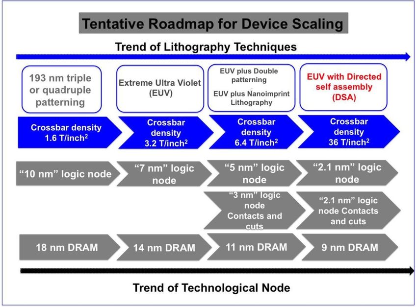
Nanotechnology 32 (2020) 012002                                                                                                    Roadmap

2. Materials consideration for emerging devices                           volume non-volatile memory products that existed in the
                                                                          marketplace.
Hao Jiang1, Thomas Mikolajick2, Damien Querlioz3 and Martin
Salinga4
1                                                                         What will be gained with further advances.      In a traditional
  Yale University, United States of America
2                                                                         computing system using von-Neumann architecture, speed
  NaMLab gGmbH and TU Dresden, Germany
3                                                                         and energy efficiency is becoming limited by the transfer of
  Université Paris-Saclay, CNRS, France
4                                                                         data via the memory bus. Therefore, approaches to move the
  Institut für Materialphysik, Westfälische
Wilhelms-Universitét Münster, Germany                                    computation closer to the memory cell itself are highly desired.
                                                                          The first step can be considered as ‘logic-in-memory’. Here,
                                                                          the computation is done directly in the memory array by using
                                                                          the stored data as one input variable and using either a suitable
Status                                                                    circuit or a pulsing scheme to realize the logical function and
                                                                          have the result remain in the memory. All resistive switching
History.   A decisive part of any machine learning system                 approaches are suitable here and also variants with ferroelec-
is the semiconductor memory. This needs to be brought as                  tric switching have been shown. In the next step, the memory
close as possible to the computing function to overcome                   device can be used to simplify the calculation of weights in
the von-Neumann bottleneck. Traditionally, all semiconductor              artificial neural networks (ANNs). Using Ohm’s and Kirch-
memories like SRAM, DRAM or EPROM or Flash memor-                         hoff’s law, analogue vector matrix multiplications can be
ies were based on the principle of charge storage. How-                   achieved in resistive memory arrays and many lab demon-
ever, since the late 1990s the efforts of using several differ-           strations have already been made using approaches based on
ent switching effects that utilize specific material properties           phase change and ionic movement [17–19]. Finally, SNNs
have increased [14], putting material science at the heart of             require both to mimic the function of a neuron and a synapse.
the research activity in non-volatile memories. Ferroelectric             Synapses have been achieved using all of the physical effects
switching, magnetic switching, phase change and memrist-                  shown in figure 3. Neurons were realized based on ferro-
ive switching based on ion movement have become the focus                 electric switching, phase change and threshold-switching type
point for research and development in new non-volatile semi-              memristive devices (e.g. based on NbOx ) [15, 20], and using
conductor memories (see figure 3). The widely used materials              the non-linear dynamics of magnetization in magnetoresist-
for ferroelectric switching, phase change and ion movement-               ive nanodevices [21, 22]. Learning-capable hardware is the
based memristive switching are traditional perovskite-based               most demanding on the material side: intense research is
(e.g. Pb(Zr,Ti)O3 ) and recently-discovered HfO2 -based fer-              still required, whereas for synapses an analogue and lin-
roelectrics, chalcogenide glass materials frequently involving            ear behaviour (see figure 4) is highly desirable [17]. Both
Ge/Te/Sb and transition metal oxides (e.g. HfO2 and TaOx ),               analogue and accumulative switching were not in the focus
respectively. For magnetic switching devices, the magnetic                of the traditional non-volatile memory device research and
layers are usually made with Fe and/or Co while MgO is typ-               development.
ically used as the tunnelling barrier layer in between. Note that
all of the mentioned physical mechanisms with the exception
of ferroelectric switching use a resistance-based readout [15].
While in ferroelectric tunnelling junctions, the material state           Status.   For a memory array utilizing one of these physical
can be read out by the resistance as well, the preferred readout          mechanisms, next to the memory cell, a selection device is
of a ferroelectric is either by measuring the switched charge or          needed to handle disturbances. The simplest version for the
by coupling the ferroelectric to a field effect transistor [16]. In       selector device is a MOS transistor, which is used in ferroelec-
the last few years, it has been established that the same mech-           tric RAMs, in magnetoresistive RAMs as well as in the avail-
anisms might be very well suited to realize functions required            able products using ion movement-based switching. How-
for machine learning. However, while for a semiconductor                  ever, using a MOSFET selector the memory cell needs to be
memory an abrupt switching with a clearly defined threshold               connected directly to the silicon. For gaining extremely high
is most favourable, the optimum switching characteristics                 densities, three-dimensional architectures, where the cells are
needed for machine learning systems are still an intense field            stacked on top of each other, have become very popular since
of research, depending on the targeted application (inference             the first introduction of 3D NAND Flash in 2013. There-
or learning) and requiring a strong link across the hierarchy             fore, other selector devices have moved into the focus of
levels starting at the material level all the way up to the sys-          research. Threshold switching devices are especially intens-
tem level. For all mechanisms mentioned above, the research               ively researched and are used in the second-generation phase
activities go back to the 1960s and the first low or medium               change memory (PCM) devices under the name of 3D cross

                                                                      8
Nanotechnology 32 (2020) 012002                                                                                                                             Roadmap

                               a)                            b)                  c)                   d)
                                                                                                                                  metal electrode
                                    +   +      +                                                                                  dielectric
                                    -   -      -                                                                                  magnetic material
                                                                                                                                  phase change material
                                            electric field             current              current             Electric field/   filament (metal or
                                                                                                                   current
                                                                                                                                  oxygen deficient oxide)

                                    -   -      -

                                    +   +      +

Figure 3. Variants of switching mechanisms used for emerging non-volatile memories. (a) In ferroelectric switching the dipoles of a
ferroelectric material are switched by an electrical field. (b) In a magnetic tunnel junction the magnetization of a free layer is switched
between the parallel and anti-parallel orientation towards a fixed reference layer. (c) In phase change memories the phase of a chalcogenide
is switched between amorphous and crystalline using joule heating and (d) in ion movement-based memories a conductive filament made of
metal atoms or oxygen vacancies is reversibly formed and ruptured.

                                                                                                ferroelectric devices, wake-up and imprint issues as well as
conductance

                                                                                      LRS       the improvement of cycling endurance require further stud-
                                                                                                ies; in phase-change-based devices, the material compositions
                                                        increasing
                                                                                                are observed to fluctuate significantly due to the high tem-
              dynamic range

                                                       non-linearity
                                                                                                peratures and strong electric fields involved in the switch-
                                                                                                ing processes; for ion movement-based memristive switching
                                                                                                devices, there are concerns over the metal electrode stability
                                                                                                and the trade-off between operation current and state retention;
                                                                                                magnetic tunnel junctions are made with multi-layers of ultra-
                                                                                                thin films, posing a serious challenge to the growth and etching
                                                                                                processes.
                                                                                                   With respect to the switching and reading characteristics,
                              HRS                                                               a strong interaction of the material centric device research
                                                                                                with the upper layer circuit and system design is required, as
                                                                             stimulus           in a machine learning system, the most suitable device char-
                                                                                                acteristics cannot be defined without looking at the system
Figure 4. SET (red curves) and RESET (green curves) of a switch                                 performance, and can depend tremendously on the targeted
for use in a synapse for SNN or a weight device for ANN. Ideal                                  application. Figure 4 summarizes one important aspect at the
characteristics for the usage as weight is added in blue.
                                                                                                single device level that has been extensively studied in the last
                                                                                                3–4 years for developing learning-capable hardware neural
point memory. Ovonic threshold switching based on chal-                                         networks and that illustrates that additional material optim-
cogenides, metal-insulator transition, and metal-ion/oxygen-                                    ization beyond the established memory function is required
vacancy movement-based switching in combination with a                                          [17]. However, also the interaction between write and read,
thermal runaway effect as observed in NbOx are all explored                                     stability aspects as well as the ability to integrate the device
in this context [15].                                                                           into an array or distributed architecture play a crucial role
                                                                                                here. Especially for inference tasks in ANNs it is important
Current and future challenges                                                                   to note that highly parallelized operation is a must. Therefore,
                                                                                                in contrast to traditional memory arrays, where a rather high
Looking forward, three important research challenges need                                       read current is necessary to achieve a fast readout, a smaller
to be solved from the material point of view: (I) tuning the                                    read current is indeed desirable. This could be an opportunity
switching and reading characteristics beyond pure memory,                                       for technologies like ferroelectric tunnel junctions that suffer
(II) scaling the device density and (III) stability and reli-                                   from a limited read current when pure memory operation is the
ability. Here stability describes the consistent behaviour or                                   task.
reproducibility of the material stack after writing opera-                                         Device scaling has shifted gears in recent years from
tions, not considering the degradation that will happen dur-                                    purely increasing the device count by reducing the dimensions
ing operation. Reliability, in contrast, describes the degrad-                                  towards using the third dimension and more and more levels
ation of the cell states during storage (retention), repeated                                   per cell. Recently in 3D NAND, 16-level devices (4 bits per
writing (endurance) or parasitic stimuli (disturbance) of the                                   cell) have entered mass production. These trends somewhat
cell. Depending on the specific device type, different mater-                                   reduce the stringent requirements for device size reduction, but
ials issues need to be solved. For example, for HfO2 -based                                     cannot make it obsolete, as the economics require achieving

                                                                                            9
Nanotechnology 32 (2020) 012002 Roadmap
the highest possible functionality per real estate. Nevertheless, consider that local fluctuations of the composition may trans-
both aspects need to be considered. The device needs to show fer to device variability. Therefore, reducing the number of
the desired behaviour at dimensions in the 10–20 nm regime, components in the active switching layer is crucial. In ferro-
which implies that the films need to be in the nm thickness electric memories, binary oxides based on HfO2 have become
range, and it must be possible to stack many layers on top much more popular compared to the traditional perovskites
of each other to achieve the necessary density for complex [16] which have at least three, but more commonly, four com-
machine learning systems. The latter implies that a selector ponents. In phase change devices, even monoatomic solu-
element not connected to the silicon bulk must be available and tions are being persued in order to create the ultimate device
that suitable deposition techniques to realize high-quality lay- [23]. Ultimately, we might need to introduce new physical
ers on materials used in standard CMOS processing are estab- mechanisms to master the challenges observed during imple-
lished. mentation. Magnetic random access memories can act as a role
Stability and reliability are traditionally the main chal- model here with the introduction of magnetic tunnel junctions,
lenges to bring a non-volatile memory into high-volume pro- spin-torque transfer, perpendicular magnetization and in the
duction. Therefore, magnetic random-access memories, phase future possibly spin orbit torque that was introduced in the
change memories and especially ion movement-based memor- last 25 years can finally be adapted by a significant number
ies have required about a decade of very intense development of semiconductor foundries.
to come up with the first niche products for the general market.
However, with respect to machine learning applications, we
need to handle even more critical issues. If we want to tailor Concluding remarks
the current-voltage characteristics to make analogue comput-
Machine learning makes non-volatile memory functions in
ing functions possible, we need to guarantee the stability to
electron devices even more important than they already are
a much higher degree compared to digital or even multi-level
today. However, the specific requirements call for modified
devices where we can rely on the high margin between differ-
or even completely new solutions. At the end of an era of
ent states.
charge storage, the prime time for material related switching
effects has finally come, making material development even
Advances in science and technology to meet more critical than it has been for traditional electron devices
challenges in the past.
The development of semiconductor devices in general and
memory devices in particular has come a long way to deliver Acknowledgments
devices with 10–20 nm feature sizes. In terms of film produc-
tion, highly reproducible techniques like atomic layer depos- The research leading to this publication has received fund-
ition have enabled the progress in the last 1–2 decades and ing from the European Research Council (ERC) under the
can still make a strong contribution to solving the challenges European Union’s Horizon 2020 research and innovation pro-
described above. Especially in scaled down devices we need to gramme (Grant Agreement Nos. 640003 and 715872).
10Nanotechnology 32 (2020) 012002 Roadmap
3. Scaling of emerging hardware and technology
for machine learning
John R Erickson1, Shuang Pi2 and Feng Xiong1
1
Department of Electrical and Computer Engineering, Uni-
versity of Pittsburgh, Pittsburgh, PA 15 261, United States of
America
2
Lam Research, Fremont, CA 94538, United States of
America
Figure 5. Working principles of PCM and ReRAM devices. Figure
Status (a) shows a cell, the active PCM area is in between a top and bottom
electrode, including a heater to induce melt/quench cycles. As heat
The human brain, which consumes only ~20 W of power is applied the active channel will change its conductivity based on
and exceeds the petaflop mark, has been the inspiration for the phase of the channel. Reproduced with permission [26]
Copyright 2010, IEEE. Figure (b) shows a typical filamentary
the next generation of computers [24]. As such, deep learn- ReRAM, as a writing current is applied to the cell, free ions move
ing and ANNs have been heavily investigated. However, together to form a connection between the top and bottom
the learning time and energy usage of these systems are electrodes. Reproduced with permission [24] Copyright 2019, John
orders of magnitude short of mimicking the brain. Part of Wiley and Sons.
the reason for this disparity in efficiency is the reliance on
traditional CMOS circuitry elements for simulating neuronal
actions, which requires bulky external memory components
leading to a large device footprint and energy consumption.
With this in mind, researchers are working towards build-
ing highly scalable hardware for ANNs that can replicate
synaptic actions through encoding analog states in their pro-
grammable conductance levels [24]. An ideal synaptic device
should offer low power, high precision, large dynamic range,
fast speed, high scalability, non-volatile retention, good endur-
ance, and low variations among many others [25]. Emer-
ging memory devices such as PCM, resistive random-access Figure 6. (a) Schematics of a crossbar array. (b) Thermal crosstalk
memory (ReRAM), conductive-bridging RAM, spin-transfer due to Joule heating in adjacent cells. Adapted with permission [27],
torque RAM, as well as electrochemical devices are all dif- Copyright 2015 Nature Publishing Group.
ferent classes of synaptic devices being investigated [24].
Limited in scope, this work will only focus on PCM and
ReRAM (figure 5), due to their relative closeness to large scale Current and future challenges
commercialization.
For ANN applications, the demanding function of vector- One formidable problem encountered in device scaling is
matrix multiplication (VMM) can be efficiently implemen- thermal crosstalk, as illustrated in figure 6(b) [27]. PCM
ted in a cross-point network [27] (figure 6(a)). The scale devices need to be elevated to a much higher temperature for
of the network, defined by the number of inputs multi- melt/quench cycles [26], requiring a large amount of energy
plied by the number of outputs, determines its computing (10–100 pJ) for switching events. This heating process can
power. Both PCMs and ReRAMs offer high device dens- unintentionally perturb the states of adjacent cells through
ity, due to the inherently small footprint of cross-point thermal crosstalk, which will only become more extensive as
cells. By further scaling these individual devices in sizes, energy densities as well as device densities get larger. Simil-
massive increases in energy efficiency, speed, and network arly, Joule heating is believed to be necessary for facilitating
density can be expected. With these improvements, large ion generation and mobility enhancement to form conduction
scale integration of ANNs into common technologies can be channels and/or modulate conductive junctions in ReRAMs.
achieved, leading to transformative advancements in machine With operation of high-density ReRAM arrays generating
learning, artificial intelligence, data analytics, internet of intensive local heating, thermal crosstalk limits the scaling
things (IoTs), and even flexible/wearable smart devices, rad- potential of ReRAM and needs to be addressed through both
ically changing the role that technology plays in everyday material engineering and overall system design to achieve bet-
life. ter thermal stability.
11Nanotechnology 32 (2020) 012002 Roadmap
Another challenge that is likely to be exacerbated with scal- To combat thermal crosstalk in ReRAM systems, small
ing is device reliability such as endurance, variation, and sta- operational currents has been demonstrated in several sub-
bility. Although individual PCM devices exhibit good endur- 10 nm material systems such as TiOx , TiOx /AlOx , HfO2 , and
ances, the stochastic nature of the melt/quench cycle can WOx [29]. Filamentary ReRAM devices typically demon-
lead to reduced device lifetimes, not only because of large strate a constant thermal heating with device scaling because
variation in individual device performances, but also due to the size of the filamentary channel remains the same with
individual device degradations like resistance drift [28]. In reduction in device dimension. However, once the device foot-
addition, phase separation in the material can cause devices print is scaled to be smaller than a typical filamentary chan-
to stick in either SET or RESET, limiting endurance [28]. nel (~10 nm), we expect to observe a limited channel growth
Aggressive scaling of PCM devices only serves to aggravate and hence a reduction in programming current and Joule heat-
these issues, as the consistency of individual device compos- ing. While these observations imply a path to begin to address
itions becomes increasingly difficult to achieve while keep- thermal crosstalk, building reliable device functionality is still
ing commercially plausible deposition rates [26]. Manufactur- challenging with higher device variability potentially asso-
ing high-density ReRAM device arrays with sufficient yield ciated with device and current scaling implied in pioneer
also becomes difficult. ReRAM fabrication usually needs an works [32, 33].Electrical forming steps can also be elimin-
etching metal layer together with multiple functional thin ated with metal particle doping and other material engineer-
films. These can generate non-volatile by-products, contam- ing techniques. These could be further facilitated with atomic
inating the critical interface and introducing numerous vari- layer deposition to precisely control thin film composition and
abilities, especially in smaller devices. In addition, as most membrane quality [29].
ReRAM materials require an electrical forming step to initial- For reducing wire resistance due to narrow interconnec-
ize conductance switching, controlling and eliminating such tions, low dimensional conductive materials such as car-
high stress processes will be critical for improving process bon nanotubes are showing progress. However, fabrication
yield. of high-density arrays remains challenging. Another solution
Finally, higher interconnection resistances from smaller is through building high aspect ratio metal electrodes with
electrode linewidths reduce the readability of the conduct- multilayer depositions, although the process is not currently
ance change in a multi-level PCM and ReRAM devices. Small commercially viable [32]. Beyond these, a 3D architecture
changes in the read current between these closely spaced con- to was demonstrated by splitting a network into vertically
ductance levels can easily be shadowed by noise [29]. In this stacked multi-layer arrays. This configuration tremendously
case, additional compensation would be required to differenti- reduces the wire resistance, as well as its footprint, but
ate these subtle differences, which will reduce either precision raises integration questions [34]. Finally, alternative fabrica-
or speed, limiting the accuracy and efficiency of a machine tion paths, including bottom up approaches as well as wafer
learning hardware based on such emerging devices. bonding methods, have been investigated and should to be
continued [32].
Advances in science and technology to meet
challenges Concluding remarks
Optimizing the thermal efficiency of cells is the first Hardware implementation of ANNs is necessary to continue
step towards improving the energy efficiency of PCM improving their performances. In this vein, several synaptic
devices and minimizing thermal crosstalk. Crosstalk typic- devices have been investigated, all with the potential for easy
ally occurs during the amorphization process, with the high integration and size scaling. PCM and ReRAM devices are
heat required for melting accidentally crystallizing neigh- discussed in this work because of their small footprint, analog
bouring amorphous cells. To minimize this risk as device conductive states, and relative technological maturity. Though
densities increase, a material with low melting temperat- both of these classes of devices have been heavily investigated,
ure and thermal conductivity can reduce the amount of heat properly managing the energy usage, thermal crosstalk, reli-
spreading during the amorphization step; whereas a high ability, and endurance of these devices remain as challenges,
crystallization temperature will increase the thermal stabil- especially as these devices attempt to be reduced to the nano-
ity of the device in the amorphous phase. Most efforts to scale dimensions. To this end, materials engineering, proper
increase the endurance of devices are focused on atomic- thermal management, and new device architectures are poten-
level engineering of these materials through the inclu- tial solutions towards these issues.
sion of dopants, though its viability in the nanoscale limit
is still indeterminate [30]. To then further improve the
endurance of PCM devices, materials with low volume Acknowledgments
changes during melt/quench cycles, as well as implementa-
tion of in-situ self-anneal heating during operations should be J.R.E. and F.X. acknowledge support through NSF Award
investigated [31]. ECCS-1901864 and CCF-1909797.
12Nanotechnology 32 (2020) 012002 Roadmap
4. Heterogeneous integration of emerging device Current and future challenges
arrays
One challenge for heterogeneous integration is the process
Peng Lin1 and Can Li2 compatibility. Many emerging devices involve an exotic
1
material stack and/or a special fabrication process that require
Massachusetts Institute of Technology, Cambridge, MA, a high temperature. Therefore, they are sometimes difficult to
United States of America be directly integrated with the mature silicon technology in
2
Department of Electrical and Electronic Engineering, The the back-end processes. A compatible monolithic integration
University of Hong Kong, Hong Kong SAR, China process generally calls for back-end-of-line (BEOL) compat-
ibility which includes strict requirements on process temper-
atures and selection of materials. While GeSbTe-based phase
Status change materials and HfOx , TaOx -based resistive switching
materials have a better back-end process compatibility, others
Neuromorphic systems based on emerging device arrays per- are not. For example, spin-transfer torque magnetic memory
form matrix multiplications following physical laws with cells use more than ten layers of crystalline ferromagnetic
high parallelism [29]. However, it is suggested that these materials [40, 41], and fabricating lithium-based electrochem-
arrays themselves, which implement the synaptic connec- ical devices require special encapsulation as lithium is highly
tions in neural networks, may not suffice the requirement reactive with silicon, therefore they are relatively challenging
of an entire hardware computing system, whereas other cir- to be compatible with existing CMOS process. Alternative to
cuit components, either implemented by conventional sil- the specifically engineered monolithic integration process, cir-
icon devices or other emerging devices, need to be hetero- cuit components could also be fabricated with different sub-
geneously integrated to fulfil the rest of functions. Building strates through technologies such as low-temperature bonding,
a complete heterogeneous system raises some new design through-silicon via interconnect, flip-chips, etc. For example,
and manufacturing challenges but would be a necessary step an image sensor array based on ‘III–V’ compounds such as
to achieve large capacity, small latencies and high energy InGaAs cannot be directly grown on CMOS substrate due
efficiency. to high process temperature but can be assembled at the
An overview of the integration roadmap is shown in fig- packaging level through low-temperature bonding [42]. How-
ure 7, where different technologies can be heterogeneously ever, these assemble methods still require delicate designs and
integrated at the device level, the array level or the func- sometimes lead to limited inter-module bandwidth caused by
tion level. First, the integration of other types of devices larger parasitic. Lastly, the compatibility of the electrical prop-
can directly enhance the electric performance of these emer- erties between different integrated devices is equally import-
ging devices in large-scale operations and applications. For ant, which requires a systematic assessment of the require-
example, the integration of selectors (such as a transistor) ments and the design capacity of each device or circuit com-
promotes the reliability and the programmability of these ponent. For example, some emerging devices require high
synaptic devices [35, 36], while a heterogeneous design of operating voltage and current and thus special design consid-
synaptic cells could facilitate high precision computing by erations are needed in designing the driving circuits especially
minimizing the intrinsic variation effects in devices [18]. with advanced silicon technology nodes.
Meanwhile, active analog circuit components can be integ- Meanwhile, although the new computing paradigm has
rated at the array level to program (‘update’) the synaptic already eliminated the movement of weight matrices within
weights stored in the emerging devices (as analog conduct- the array, efficient data movement between arrays is still
ances or capacitances), and/or sense (‘inference’) the output. highly desired for large neural network applications. The
Recently, demonstrations with integrated on-chip program- efforts could involve optimized architecture designs such as
ming/sensing peripherals have shown encouraging results local cache or global memory for storing temporal data, shared
[37, 38]. Moreover, the peripherals’ functions are not lim- data bus or dedicated one-by-one connections between arrays
ited to accessing individual devices in an array. Neural net- and tiled arrays for different network topologies [43]. Mean-
work functions such as non-linear activations and pooling while, developing efficient analog circuits for hardware func-
can also be physically integrated at the array output and tions, such as non-linear activations and pooling functions,
keep data movement locally. A promising approach would be while keeping all the signals in the analog domain locally for
harvesting the rich physical properties in emerging devices, inter-array communication, could significantly boost the effi-
which can potentially offer much improved speed and power ciency to the next level if successful.
efficiency as compared with the mature silicon technology
[39]. Finally, in favor of emerging edge computing applic-
ations, the computing device arrays can be directly integ- Advances in science and technology to meet
rated with sensors, actuators, photonics, RF and control challenges
logics circuits with minimum communication and control
overheads thus promise the real-time and low power edge First, the performance of the emerging system can still be
processing [40]. largely affected by the device performance. Improvement of
13Nanotechnology 32 (2020) 012002 Roadmap
Figure 7. Roadmap of heterogenous integration of emerging device arrays.
device performance (with compatible fabrication conditions) ibly stacked up (such as oxide-based memristors). The imme-
can significantly enhance the computing capability of these diate benefit of a 3D system is shorter connection length and
systems, and the figures of merits include the device uniform- higher density. Different technologies can also be stacked on
ity, the analog conductance tuning linearity, the data reten- top of each other, promising significantly reduced system foot-
tion, and the re-programming endurance. Some effective solu- print, improved communication bandwidth (2D area interface
tions include advances in material engineering [44] or new cell as opposed to the 1D edge interface in 2D systems) and exten-
designs with the integration of mature technologies [18]. ded functionalities.
Second, there is plenty of room to optimize the peripher-
als circuitry for higher energy efficiency and a smaller foot-
print targeting a specific scenario. The different requirements Concluding remarks
of a neuromorphic system, such as low precision and a spe-
cific voltage and current level may call for entirely different The heterogeneous integration of different emerging techno-
designs. Meanwhile, different array operating methods could logies is a key step towards the large-scale system integ-
be carefully compared and chosen, such as using pulse width ration and applications. The performance and efficiency
or pulse amplitude for analog signal representation. In addi- of the system with all parts combined require careful
tion, emerging devices with various non-linear behaviors may designs and optimizations. While promising proof-of-concept
promise completely new designs and novel functions to be het- demonstrations were reported, challenges still exist in the
erogeneously integrated and replace the conventional silicon integration process development, electrical compatibilities
devices and circuits entirely, with each device serving a unique optimization and architectural designs for minimized data
functionality. movement/conversion in modern neural networks. Extens-
Finally, more efficient data communications can be imple- ive research efforts are underway to develop new emerging
mented by new fabrication processes, new architectures, new device types with unique functionalities and smart circuit and
array designs and more. For example, fabrication methods and array design with 3D integration are being investigated to
array designs that reduce the wire resistances of the array can make the system more efficient. The heterogeneous integra-
greatly promote the programming and inference precisions tion of a wide spectrum of emerging devices, with new array
and mitigate the sneak path issues in passive (transistorless) and architecture designs promises the disruptive computing
arrays. 3D integration [45] of a heterogeneous system is a power for future machine learning and artificial intelligence
favorable option as a lot of emerging devices can be compat- systems.
14Nanotechnology 32 (2020) 012002 Roadmap
5. The processing strategies for memristor Current and future challenges
crossbar fabrication
The continued downscaling of nanoelectronic devices imposes
Yu Chen and Shisheng Xiong ever-more stringent requirements on the strategy used to
achieve ultra-small feature size while maintaining low
School of Information Science and Technology, Fudan
defectivity. Along with the previous success of memristor-
University
based AI chips, it is becoming imperative to continue to
increase the crossbar density for better network performance.
Status The main challenges experienced in the scaling process of
crossbar fabrication include the selection of proper processing
While the need for mobile and fast computing in a smart soci- strategies for sub-10 nm patterning, the increase in integration
ety is ever growing, the semiconductor industry has been fail- difficulty, and the potential for performance degradation of the
ing to exploit the power and efficiency provided by device scal- miniaturized devices.
ing. Currently, we are witnessing a divergence of paths for Current chip-level crossbar arrays are made at the µm level
future computing, with non-von Neumann architectures that with conventional photolithography. Direct writing tools, such
are anticipated to significantly disrupt traditional CMOS tech- as EBL, are able to deliver high-resolution patterning, but
nology. For example, commercial digital AI chips (TrueNorth are not ideal for mega-scale crossbar fabrication due to their
and Loihi) developed by IBM and Intel, respectively, colloc- extremely time-consuming writing procedure [49]. Further-
ated the memory and processing units for a reconfigurable more, the small critical dimension of a crossbar causes the
design. Recently, memristor-based analogue computing has performance of the final device to be vulnerable to process
been the focus of intensive research. Memristors arranged in variation. Therefore, it is critical to simultaneously optim-
a crossbar array provide a two-dimensional representation of ize all the processing steps to reduce the defectivity and to
a neural network, and have the advantages of greatly maxim- enhance the pattern transfer uniformity. In addition, system-
izing the device area density (2N lines and N2 devices) and level integration requires reliable 3D integration of crossbar
unifying logic and memory for IMC. analogue or hybrid chips arrays with underlying CMOS circuits. Direct fabrication of
based on this network have proven to be extremely efficient crossbar arrays on a foundry-developed CMOS chip should
(computing power efficiency up to over 10TOPS per watt) guarantee precise alignment and a low thermal budget [50].
for pattern classification or online training of neural network Another big challenge associated with crossbar scaling is
algorithms [29]. At a fundamental level, this novel hardware the increasing density of local interconnects. The resistance
can act as a dot-product engine for running VMM operations, of these non-ideal interconnects increases as the size shrinks,
which are very frequently used in deep learning algorithms causing a significant voltage drop across the array. This phe-
[35]. nomenon will severely disturb the functionality of memristor
Since the first memristor device was made in HP Labs crossbar arrays, resulting in insufficient power supply on indi-
in 2008, different patterning techniques have been employed vidual devices and a large error rate during write/read opera-
for memristor crossbar fabrication. Electron beam lithography tions [51]. Other problems include more device-to-device vari-
(EBL) is more frequently used for patterning crossbar arrays ation and current interference between more densely packed
at high resolution, but over a relatively small area [46]. neighboring cells, known as the sneak path current problem
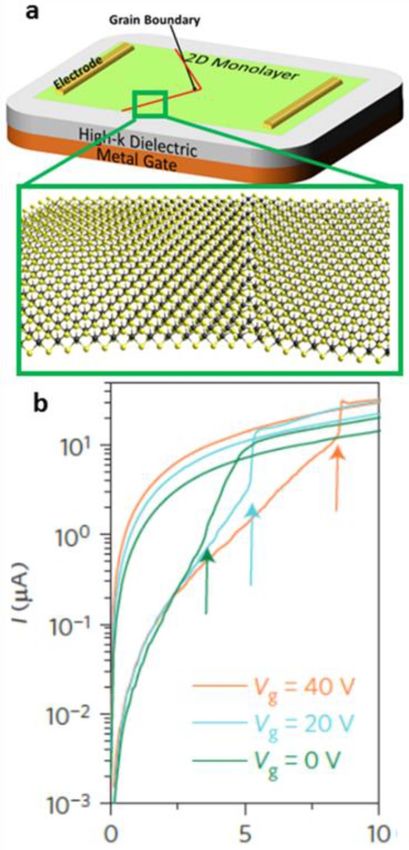
Newly emerging techniques, including extreme ultraviolet [52]. Although there is no description of the benchmark for
(EUV) lithography, nanoimprint lithography (NIL) and dir- defect density in the literature, the essence of neural network
ected self-assembly (DSA), have been listed in the Interna- indicates that the defectivity level of a crossbar array can be
tional Roadmap for Devices and Systems (IRDS) as advanced higher than it can be for the logic chips, which are permitted
lithography techniques for device fabrication at the 3–5 nm less than 100 defects per cm2 [29]. The strategies to realize
technology node (figure 8) [47]. So far, direct templating with high-throughput manufacturing of large-scale, high-density
DSA (coupled with NIL) for the fabrication of bit patterned crossbar arrays and integrated systems rely on the continued
media with a crossbar structure has achieved a device density efforts to explore new patterning methodologies, as well as a
greater than 1T inch−2 [48]. The high-throughput advanced collaborative effort between academia and industry.
lithography techniques (e.g. EUV) will penetrate into the man-
ufacturing once the market size and the fabrication cost are
leveraged. For reference, in figure 8 we have listed the estim- Advances in science and technology to meet
ated device density of passive crossbar arrays fabricated with challenges
the corresponding processing strategies. Considering the foot-
print of accessing devices, the cell area with respect to dif- Both academia and industry are making long-term endeavors
ferent architectures would be 8- or 4- fold larger: ~8F2 for to realize the fabrication of large-scale, high-density
one-transistor, one-resistor architecture (1T1R), 4F2 for one- crossbar arrays for production. EUV is a commercial-
selector, one-resistor architecture (1S1R), where F is the half ized, high-resolution lithography technique for high-volume
pitch. manufacturing in the semiconductor industry, which greatly
15You can also read