Roadmap on quantum nanotechnologies - Nanotechnology - IOPscience
←
→
Page content transcription
If your browser does not render page correctly, please read the page content below
Nanotechnology

ROADMAP • OPEN ACCESS

Roadmap on quantum nanotechnologies
To cite this article: Arne Laucht et al 2021 Nanotechnology 32 162003

View the article online for updates and enhancements.

                               This content was downloaded from IP address 46.4.80.155 on 26/03/2021 at 08:25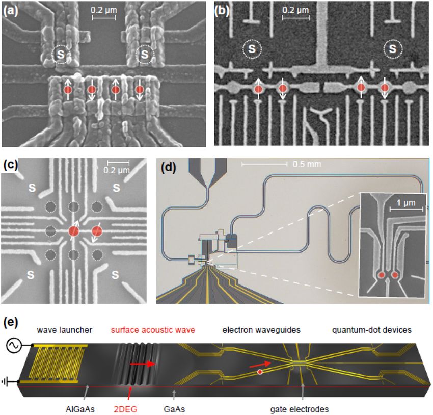
Nanotechnology
Nanotechnology 32 (2021) 162003 (48pp) https://doi.org/10.1088/1361-6528/abb333
Roadmap
Roadmap on quantum nanotechnologies
Arne Laucht1,*, Frank Hohls2, Niels Ubbelohde2, M Fernando Gonzalez-Zalba3,4,
David J Reilly5,6, Søren Stobbe7, Tim Schröder8,9, Pasquale Scarlino10, Jonne V
Koski10, Andrew Dzurak1, Chih-Hwan Yang1, Jun Yoneda1, Ferdinand Kuemmeth11,
Hendrik Bluhm12, Jarryd Pla13, Charles Hill14, Joe Salfi15, Akira Oiwa16,17,18,
Juha T Muhonen19, Ewold Verhagen20, M D LaHaye21,22, Hyun Ho Kim23,24, Adam W
Tsen23, Dimitrie Culcer25,26, Attila Geresdi27, Jan A Mol28, Varun Mohan29,
Prashant K Jain30,31,32,33 and Jonathan Baugh23
1
Centre for Quantum Computation and Communication Technology, School of Electrical Engineering
and Telecommunications, UNSW Sydney, New South Wales 2052, Australia
2
Physikalisch-Technische Bundesanstalt, 38116, Braunschweig, Germany
3
Quantum Motion Technologies, Nexus, Discovery Way, Leeds, LS2 3AA, United Kingdom
4
Present address: Quantum Motion Technologies, Windsor House, Cornwall Road, Harrogate HG1 2PW,
United Kingdom
5
School of Physics, University of Sydney, Sydney, NSW 2006, Australia
6
Microsoft Corporation, Station Q Sydney, University of Sydney, Sydney, NSW 2006, Australia
7
Department of Photonics Engineering, DTU Fotonik, Technical University of Denmark, Building 343,
DK-2800 Kgs. Lyngby, Denmark
8
Department of Physics, Humboldt-Universität zu Berlin, 12489, Berlin, Germany
9
Ferdinand-Braun-Institut, Leibniz-Institut für Höchstfrequenztechnik, 12489 Berlin, Germany
10
Department of Physics, ETH Zürich, CH-8093, Zürich, Switzerland
11
Niels Bohr Institute, University of Copenhagen, 2100, Copenhagen, Denmark
12
JARA-FIT Institute for Quantum Information, RWTH Aachen University and Forschungszentrum
Jülich, 52074, Aachen, Germany
13
School of Electrical Engineering and Telecommunications, UNSW Sydney, New South Wales 2052,
Australia
14
School of Physics, University of Melbourne, Melbourne, Australia
15
Department of Electrical and Computer Engineering, The University of British Columbia, Vancouver
BC V6T 1Z4, Canada
16
The Institute of Scientific and Industrial Research, Osaka University, Ibaraki, Osaka 567-0047, Japan
17
Center for Quantum Information and Quantum Biology, Institute for open and Transdisciplinary
Research Initiative, Osaka University, 560-8531, Osaka, Japan
18
Center for Spintronics Research Network (CSRN), Graduate School of Engineering Science, Osaka
University, Osaka 560-8531, Japan
19
Department of Physics and Nanoscience Center, University of Jyväskylä, FI-40014 University of
Jyväskylä, Finland
20
Center for Nanophotonics, AMOLF, 1098 XG, Amsterdam, The Netherlands
21
Department of Physics, Syracuse University, Syracuse, NY 13244-1130, United States of America
22
Present Address: United States Air Force Research Laboratory, Rome, NY 13441, United States of
America
23
Institute for Quantum Computing, University of Waterloo, Waterloo, Ontario N2L 3G1, Canada
24
School of Materials Science and Engineering & Department of Energy Engineering Convergence,
Kumoh National Institute of Technology, Gumi 39177, Korea
25
School of Physics, The University of New South Wales, Sydney 2052, Australia
26
Australian Research Council Centre of Excellence in Future Low-Energy Electronics Technologies,
UNSW Node, The University of New South Wales, Sydney 2052, Australia
27
QuTech and Kavli Institute of Nanoscience, Delft University of Technology, 2600 GA Delft, The
Netherlands
Original content from this work may be used under the
terms of the Creative Commons Attribution 4.0 licence. Any
further distribution of this work must maintain attribution to the author(s) and
the title of the work, journal citation and DOI.
1361-6528/21/162003+48$33.00 1 © 2021 The Author(s). Published by IOP Publishing Ltd Printed in the UK
Nanotechnology 32 (2021) 162003                                                                          Roadmap

28
   School of Physics and Astronomy, Queen Mary University of London, E1 4NS, United Kingdom
29
   Department of Materials Science and Engineering, University of Illinois at Urbana-Champaign,
Urbana, IL 61801, United States of America
30
   Department of Chemistry, University of Illinois at Urbana-Champaign, Urbana, IL 61801, United
States of America
31
   Materials Research Laboratory, University of Illinois at Urbana-Champaign, Urbana, IL 61801, United
States of America
32
   Department of Physics, University of Illinois at Urbana-Champaign, Urbana, IL 61801, United States
of America
33
   Beckman Institute for Advanced Science and Technology, University of Illinois at Urbana-Champaign,
Urbana, IL 61801, United States of America
*
  Author to whom any correspondence should be addressed.

E-mail: a.laucht@unsw.edu.au

Received 8 October 2019
Accepted for publication 27 August 2020
Published 4 February 2021

Abstract
Quantum phenomena are typically observable at length and time scales smaller than those of
our everyday experience, often involving individual particles or excitations. The past few
decades have seen a revolution in the ability to structure matter at the nanoscale, and
experiments at the single particle level have become commonplace. This has opened wide new
avenues for exploring and harnessing quantum mechanical effects in condensed matter. These
quantum phenomena, in turn, have the potential to revolutionize the way we communicate,
compute and probe the nanoscale world. Here, we review developments in key areas of quantum
research in light of the nanotechnologies that enable them, with a view to what the future holds.
Materials and devices with nanoscale features are used for quantum metrology and sensing, as
building blocks for quantum computing, and as sources and detectors for quantum
communication. They enable explorations of quantum behaviour and unconventional states in
nano- and opto-mechanical systems, low-dimensional systems, molecular devices,
nano-plasmonics, quantum electrodynamics, scanning tunnelling microscopy, and more. This
rapidly expanding intersection of nanotechnology and quantum science/technology is mutually
beneficial to both fields, laying claim to some of the most exciting scientific leaps of the last
decade, with more on the horizon.
Keywords: nanotechnology, quantum phenomena, quantum computing, quantum
electrodynamics
(Some figures may appear in colour only in the online journal)

                                                                   2
Nanotechnology 32 (2021) 162003                                               Roadmap

Contents

 1. Metrology and sensing                                                          5
    1.1. Electrical quantum metrology with single electrons                        5
    1.2. Fast dispersive readout for solid-state qubits                            7
 2. Quantum light sources, cavities and detectors                                 10
    2.1. Quantum light sources                                                    10
    2.2. Semiconductor–superconductor hybrid circuit-QED                          13
 3. Quantum computing with spins                                                  15
    3.1. GaAs quantum dots                                                        15
    3.2. Quantum computing with spins in silicon: dots                            18
    3.3. Quantum computing with donor spins in silicon                            20
    3.4. Single-atom qubits: acceptors                                            23
    3.5. Quantum interface based on photon-spin coherent transfer                 25
 4. Nano and opto-mechanics                                                       28
    4.1. Opto- and electromechanical transduction                                 28
    4.2. Quantum nanomechanics                                                    30
 5. Low-dimensional systems                                                       33
    5.1. Quantum tunneling devices incorporating 2D magnetic semiconductors       33
    5.2. Topological states                                                       35
 6. Molecular devices                                                             38
 7. Nanoplasmonics                                                                40
References                                                                        44

                                                          3
Nanotechnology 32 (2021) 162003                                                                                                  Roadmap

Introduction                                                             resonators, for the purpose of spin readout, remote spin–spin
                                                                         coupling, and semiconductor–superconductor hybrid quantum
The year 2019 marks the 60th anniversary of Richard Feyn-                devices.
man’s seminal lecture ‘There’s Plenty of Room at the Bottom:                 In section 3 we are discussing quantum computing with
An Invitation to Enter a New Field of Physics’ at the California         spins in the solid state. Electronic spins have shown to
Institute of Technology on 29 December 1959. In his lecture,             be highly-coherent quantum systems that promise to be
Feynman considered the possibilities of directly manipulating            scalable to a large number of qubits in very little space
individual atoms, designing microscopes with atomistic resol-            when integrated in a semiconductor platform. The four
ution, and building nanoscale machines. His talk was very vis-           contributions in this section cover different implementa-
ionary and sparked many ideas that can be classified as nano-            tions. The first two contributions make use of quantum
technology, although the actual term was not coined until some           dots (QDs) in the electrostatically-defined potential of nano-
20 years later and the field of nanotechnology did not emerge            structures in gallium-arsenide (GaAs)-based material sys-
as a research direction until the 1980s. Around this time, in            tems by Ferdinand Kuemmeth and Hendrik Bluhm, and in
1989, it was also when the IOP journal Nanotechnology was                silicon-based material systems by Andrew Dzurak, Chih-
founded, and thus the year 2019 coincidentally also marks the            Hwan Yang and Jun Yoneda. The other two contributions look
journal’s 30th anniversary. All of this is more than enough              at more naturally-confined spin systems, namely donor spins
reason to reflect on some of the contributions that nanotech-            in silicon by Jarryd J Pla and Charles Hill, and acceptor spins
nology has made to science in recent years. In this Roadmap              in silicon by Joe Salfi.
article, we would like to take a closer look at the importance               Section 4 covers the topic of Nano- and opto-mechanics.
of nanotechnology to shape the field of quantum systems by               Here, Juha Muhonen and Ewold Verhagen discuss the coup-
reviewing the state-of-the-art in a number of different subfields        ling of mechanical resonators to electromagnetic fields, and
from metrology, quantum communication, quantum computa-                  illuminate how mechanical resonators can be used as a trans-
tion, to low-dimensional systems.                                        ducer to convert quantum signals from one electromagnetic
    This Roadmap is structured similarly to other Roadmaps               mode to another, as e.g. from microwave frequencies to optical
that have been published on e.g. magnetism [1] and plasma                frequencies. Matthew D LaHaye then writes about quantum
physics [2]. Each section is written by experts in their fields          nanomechanical systems that allow fundamental explorations
and tries to capture the state-of-the-art as well as outline some        of motion and quantum thermodynamics with applications in
of the future challenges and research directions.                        quantum computation, communication, sensing, and hybrid
    In section 1 on Metrology and sensing we have two con-               quantum platforms.
tributions. The first one by Frank Hohls and Niels Ubbelo-                   Section 5 is dedicated to low-dimensional systems. In their
hde details how semiconductor nanodevices can be used to                 contribution Hyun Ho Kim and Adam W Tsen discuss CrI3 as
deterministically shuttle single electrons with high frequency           an example of a 2D semiconductor with magnetic properties
to redefine the ampere in units of time and the elementary               that exhibits strong tunnel magnetoresistance (TMR) when
charge. In some sense this is a perfect example of a nanoma-             used in a quantum tunneling device, with applications in spin
chine as Feynman might have envisioned it—it is an apparatus             filters and for magnetic memories. Dimitrie Culcer and Attila
that can move individual electrons. The second contribution by           Geresdi then write about topological states and how they can
M Fernando Gonzalez-Zalba and David J Reilly then shows                  be exploited for dissipationless transport at low temperatures,
how proper use of classical microwave engineering allows the             spin–orbit torque devices at room temperature and topologic-
detection of a single charge movement in a nanodevice, which             ally protected quantum electronics in general.
in combination with Pauli spin blockade even allows the detec-               In section 6, Jan Mol reports on the progress in molecular
tion of a single spin state.                                             devices, where the unique properties of individual molecules
    Section 2 on Quantum light sources, cavities and detect-             are exploited to build functional electronic devices. In partic-
ors takes a closer look at the interaction of quantum systems            ular, molecular designs allow for the engineering of optical,
with photons. Søren Stobbe and Tim Schröder review quantum               magnetic and quantum effects that are not readily achiev-
light sources, their properties, and their ability to emit various       able in lithographically defined nanostructures. And finally,
quantum states of light. Quantum light sources play an import-           in section 7 on nanoplasmonics, Varun Mohan and Prashant
ant role for quantum communication and complex photonic                  K Jain discuss the high-localization of electromagnetic fields
quantum systems. Akira Oiwa then extends the discussion to               using nanoplasmonic structures that allow the spatiotem-
long-distance quantum networks that rely on quantum repeat-              poral concentration of optical energy far below the dif-
ers based on coherent quantum interfaces between static qubits           fraction limit of light. These effects can be exploited for
(solid-state spins) and flying qubits (photons). Long-distance           highly-efficient single photon sources, enhanced photocata-
entanglement is required for distributed quantum computing               lytic conversion, and all-optical nanoplasmonic circuits for
as well as a secure quantum internet. The third contribution by          computation.
Pasquale Scarlino and Jonne V Koski discusses the coupling                   Jonathan Baugh and Arne Laucht
of charges and spins to photons in superconducting microwave                 Editors of the Roadmap on Quantum Nanotechnology

                                                                     4
Nanotechnology 32 (2021) 162003                                                                                                          Roadmap

1. Metrology and sensing

1.1. Electrical quantum metrology with single electrons

Frank Hohls and Niels Ubbelohde
Physikalisch-Technische           Bundesanstalt,   Braunschweig,
Germany

1.1.1. Status.   The generation of a quantized electric current
I = ef by single-electron (SE) control with e the elementary
charge and f the repetition frequency was suggested soon after
the first demonstrations of SE devices [3, 4]. Initially, in series
connected metallic SE transistors (SETs) were pursued, cumu-
lating in a SE current source built of six SETs with error prob-
ability 1.5 × 10⁻⁸ , albeit at a current level of only 0.81 pA,
limited by the tunnelling barriers with fixed transparencies [3].
SE pumps (SEPs) with higher current levels can be realized
using semiconductor QDs, where the SE tunnelling rates can                Figure 1. Example of quantized single-electron current generated
be varied [5]. These tunable-barrier SEPs are also less com-              by a quantum dot SEP as function of control voltage (f = 600 MHz,
plex to operate, requiring only two control gates and a single            B = 9.2 T, ef = 96.130600). Schematic upper right: QD with gate
time-dependent drive signal, and operate up to several GHz                controlled tunnelling barriers. Lower schematic: pumping cycles: (i)
                                                                          electron loading, (ii) isolation and (iii) ejection to drain. Inset plot
driving frequency [6]. The research on SEPs also pushed the               left: high accuracy measurement of current deviation from ef; right:
development of improved current measurement capabilities [5,              histogram of 1 h measurement points shown in red. Average −0.1
7]. This allowed in recent years to confirm the quantization              ppm agrees with ef within uncertainty 1.6 × 10⁻⁷ . Graph adopted
accuracy for several GaAs and silicon based SEPs operated at              from [8].
f ⩾ 0.5 GHz at sub-ppm relative uncertainty [7, 8] (example in
figure 1).
    Since 20 May 2019 the International System of Units                       The short time scales of charge transfer at frequencies in
(SI) is fully defined by a set of fundamental constants with              the regime of ∼ 1 GHz makes it difficult to directly resolve the
fixed values [9], among them the elementary charge e =                    success rate of isolating and subsequently transferring single
1.602176634 × 10⁻¹⁹ As. In this new SI SEPs are now the                   electrons in QDs and the rarity of errors in this residually
shortest path to a representation of the unit Ampere, using               still stochastic process necessitates new concepts and improve-
only e and a frequency f derived from the hyperfine split-                ments to the sensitivity of charge and current detection.
ting of Caesium. The alternative path combines two quantum                    A further increase in the current level towards the
effects, the quantum Hall effect (QHE) and the Josephson                  nanoampere regime is required for metrological applications
effect, which both incorporate an additional fundamental con-             at accuracies better than 10−7 and poses another challenge,
stant, the Planck constant h. The realization of a suitable               which can be addressed by an increase in excitation frequency
SE based primary current standard would impact both the                   or device parallelization. However, all realizations of SEPs,
metrological practice and the fundamentals of metrology:                  that have so far shown good (sub-ppm) accuracy, were prone
Firstly, it would allow to improve the measurement accuracy               to strong degradation when operated beyond 1 GHz [7]. Sim-
for small currents, relevant e.g. in semiconductor technology             ilarly, the reproducibility of tunnel coupled dynamic QDs as
and environmental sensing. Secondly, a comparison between                 needed for parallelization is not yet understood.
the quantized currents generated along the two mentioned                      The above challenges have to be solved to provide the
paths (‘Quantum Metrology Triangle’ [3, 4], figure 2(b)) with             single electron path for the test of the fundaments of electrical
sufficiently increased accuracy would test the fundament of               quantum metrology at the desired uncertainty level of 10−8 .
electrical quantum metrology.                                             In addition, this test requires also large improvements for a
                                                                          current comparison based on the second leg, where the QHE
                                                                          and the Josephson effect are used to generate resp. measure
1.1.2. Current and future challenges.      The most important             a quantized current of only ∼ 1 nA or less. This requires at
task in the development of a primary quantum standard based               least one order of magnitude improvement compared to the
on SEPs is to establish the universality of the current to fre-           best present techniques.
quency relation, which relies on the manipulation of tunnelling
rates over many orders of magnitude. The robustness of the
operating principle in the presence of disorder and potential             1.1.3. Advances in science and technology to meet chal-
fluctuators and a fundamental understanding of the dynamics               lenges. To demonstrate the universality of SEPs advances
of electronic transport under high frequency excitation, includ-          will necessitate the validation of current quantization at
ing the role of electron spin and magnetic field, are both exper-         accuracies better than 10−8 . Comparative measurement of
imentally and theoretically very challenging questions [4, 5].            multiple SEPs could be realized by either a null measurement

                                                                      5
Nanotechnology 32 (2021) 162003                                                                                                     Roadmap

                                                                               Device technology has to be developed to increase SEP
                                                                           accuracy by maximizing charging energy and sharp transi-
                                                                           ents in the time-dependent tunnelling rates. While GaAs is
                                                                           presently the most reliable technology basis for high accur-
                                                                           acy SEPs, silicon based SEPs, especially by utilizing strong
                                                                           SE confinement in trap states [6], have shown the potential for
                                                                           higher frequency. However, a large increase of the presently
                                                                           much too low yield in the fabrication of silicon SEPs is needed.
                                                                           The desired combination of large-bandwidth charge detectors
                                                                           with SEPs into integrated single electron circuits featuring in-
Figure 2. (a) Schematic for in-situ validation of SEP universality.        situ detection sets additional demands on device stability and
Two SEPs are connected in series and operated at the same                  reproducibility.
frequency. Any difference in the generated SEP currents can be
measured either by a charge Q built up on an isolated node in                  Parallelization is very likely to rely on the ability to indi-
between the SEPs or by an error current I err through a lead tapping       vidually address the QD devices forming the parallel network.
the node. (b) The two possible primary realizations of a current           Complex connection circuitry and the availability of a high
standard. The left SEP path allows direct transfer from a frequency        count of individual dc control voltages is therefore required
(derived from a primary frequency standard) to a current. The right        but might benefit by developments towards scalable quantum
path uses Ohms law with a quantized voltage generated by the
Josephson effect and a quantized resistance by the quantum Hall            bit circuits based on semiconductor QDs.
effect. A comparison of the currents generated along                           These advances in technology are also necessary for the test
the two paths realizes the ‘Quantum Metrology                              of the fundaments of electrical quantum metrology by compar-
Triangle’.                                                                 ing the SE current to the combination of QHE and Josephson
                                                                           effect at 10−8 accuracy (figure 2(b)).

of the differential current or an in-situ validation detecting
                                                                           1.1.4. Concluding remarks.     In the recent years large pro-
the charge trapped on an island between two current sources
                                                                           gress has been achieved towards a SE based primary current
(figure 2(a)).
                                                                           standard. However, impact and application of SEPs in met-
    Towards this goal multiple technological capabilities have
                                                                           rology has been hampered by the missing validation of uni-
to be achieved: to acquire a statistical basis large enough to
                                                                           versality and robustness of the current to frequency relation.
verify rare quantization errors would require in the case of
                                                                           Additionally increasing the current will broaden the applic-
charge detection a detector bandwidth in excess of 100 kHz
                                                                           ation range and widen the impact on practical metrology.
with correspondingly low identification errors or in the case of
                                                                           Finally, adding the connection to QHE and Josephson effect
direct current verification noise levels in the very low fA/rtHz
                                                                           would allow to test and strengthen the fundament of electrical
range and a current level in the nanoampere range with consid-
                                                                           quantum metrology.
erable demands to the overall stability of the experiment. Sim-
ilar improvements are needed for the transfer accuracy from                Acknowledgments
QHE and Josephson effect to a current of ∼ 1 nA, where for                 We acknowledge funding under EMPIR project ‘SEQUOIA’
this path to a primary current source the low level of current is          17FUN04, co-funded by the EU’s Horizon 2020 programme
demanding.                                                                 and the EMPIR Participating States.

                                                                       6
Nanotechnology 32 (2021) 162003                                                                                                      Roadmap

1.2. Fast dispersive readout for solid-state qubits

M Fernando Gonzalez-Zalba1 and David J Reilly2
1
    Hitachi Cambridge Laboratory, United Kingdom
2
    Institute for Microsoft Corporation and University of Sydney

1.2.1. Status.    A qubit specific measurement readout pro-
tocol is an essential ingredient for all quantum computing tech-
nologies. The minimum time required to perform a measure-
ment (tmin ) is an important characteristic of the method as for
high-fidelity qubit detection, readout has to be faster than the
relaxation time of the system (T 1 ). Moreover, to implement
fast feedback in error correction protocols, the readout must
be faster than the intrinsic decoherence time (T 2 ). Another          Figure 3. Readout fidelity as a function of integration time. The
important aspect is that the time needed to determine the qubit        varying parameters are the relaxation time T 1 and the minimum
state is bounded by quantum mechanics and hence it is always           integration time tmin defined as the integration time to achieve a
                                                                       signal-to-noise ratio of 1. The red areas indicate integration times
longer or at best equal to half the dephasing time induced by          for tmin = 100 ns and T 1 = 10 ms where high fidelity readout
the back-action of the detector (tφ ).                                 (>99%) cannot be obtained.
    For superconducting charge qubits, semiconductor-based
qubits and Majorana zero modes, one can use charge sensors
such as the quantum point contact or the single-electron tran-         roadmap for silicon spin qubits implemented in double QDs
sistor (SET)—with charge sensitivities of a fraction of an elec-       (DQDs) that offer some of the longest coherence times of
tron charge—to detect the charge, spin or parity state of these        all solid-state device platforms while being manufacturable at
qubits which can be achieved either via direct charge readout          scale using very large-scale integration processes.
or via spin- or parity-to-charge conversion, respectively. How-
ever, the direct current (DC) versions of these sensors have an
upper bandwidth limit of a few tens of kHz. High-frequency             1.2.2. Current and future challenges.        The challenge for dis-
techniques have been developed to overcome these limita-               persive sensing is to increase the readout fidelity well above
tions. By embedding the sensor in a LC tank circuit, single            99% in timescales shorter than T 2 setting a clear target on the
electron resolution with a bandwidth in excess of 100 MHz              integration time (tint ) of a measurement. Following the readout
has been reached. However, the radiofrequency (RF) SET,                model of Barthel et al [15], and assuming white noise, we
the most sensitive of all charge sensors, does not reach the           find a useful rule of thumb for dispersive sensor designers:
quantum limit for detection due to the induced measurement             T 1 /25 > tint > 25 tmin that translates in a necessity to increase
back-action caused by the randomness of the charge tun-                the T 1 /tmin ratio, see figure 3. In this roadmap, we focus on
nelling processes. The roadmap for the radio frequency RF-             technological advances to minimize tmin . See section 3.1 for a
SET is well known and hence will not be subject to further             discussion on increasing T 1 . The minimum measurement time
discussion [10].                                                       of an impedance matched dispersive sensor, defined here as the
    More recently, research has been shifting towards dis-             integration time to achieve a signal-to-noise ratio of one, can
persive readout methods in which the qubit to be sensed is             be estimated in the small signal regime using the steady-state
coupled non-resonantly to a high-frequency electrical reson-           approximation [16, 17]:
ator [11, 12]. In this paradigm, the state-dependent react-
ance of the qubit manifests in a difference in the reflec-                                                        (         )
                                                                                                       kB TN          Cr
tion or transmission coefficient of the resonator. Dispersive                                 tmin ∝          2
                                                                                                                                           (1)
                                                                                                       (αe)           Qωr
readout approaches the quantum limit, yields high-fidelity sub-
microsecond measurement times, and does not require addi-
tional sensing elements, simplifying the overall qubit archi-              Equation (1) highlights the different levels where readout
tecture. The method is extensively used to read supercon-              fidelity improvements can be accomplished: At the device
ducting qubits in a single-shot manner, and more recently to           level, by increasing the coupling α to inter-dot charge trans-
detect the spin parity of singlet-triplet qubits in silicon with       itions. Geometrically, α corresponds to the difference between
up to 98% fidelity in 6 µs [13]. Finally, there are propos-            the ratios of the coupling capacitance of the resonator to each
als to extend this methodology to enable parity detection of           QD and their total capacitance. At the resonator level, by
Majorana bound states by parity-dependent hybridization to a           increasing its natural frequency of resonance (ωr ), increas-
quantum dot (QD) [14].                                                 ing its loaded quality factor (Q) and reducing its capacitance
    Given the different relaxation times, the technical require-       (Cr )—or
                                                                              √ in other words by increasing the resonator impedance
ments to achieve readout fidelities above error-correction             Zr = Lr /Cr at fixed ωr . Finally, at the amplification level, by
thresholds vary across platforms. Although our discussion              reducing the noise temperature of the first amplifying stage
will be of general applicability, when specific, we tailor our         (TN ).

                                                                   7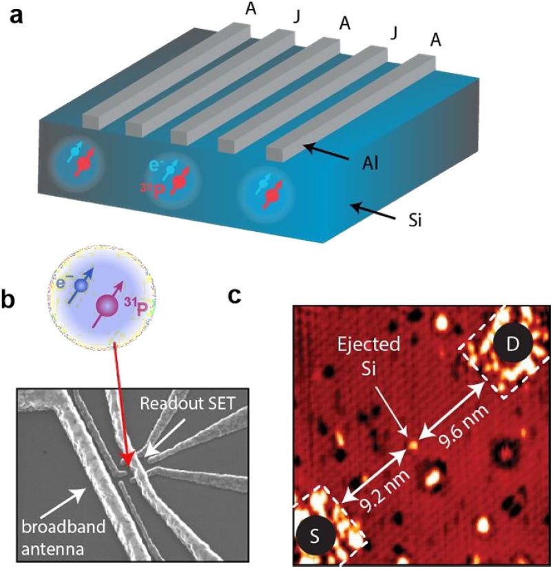
Nanotechnology 32 (2021) 162003                                                                                                       Roadmap

                                                                             by using thin (10 nm) silicon-on-insulator (SOI) and/or using
                                                                             non-planar gate geometries. However, 3D geometries may
                                                                             complicate QD couplings in 2D and therefore fabrication
                                                                             advances and design of novel qubit arrays will have to be pro-
                                                                             posed. Finally, a large gate coupling to inter-dot transitions can
                                                                             be achieved by minimizing cross coupling capacitance of the
                                                                             sensing gate or by driving the DQD gates in differential mode.
                                                                                 At the resonator level, the field will benefit from mov-
                                                                             ing to on-chip lumped-element MW resonators where, by
                                                                             increasing the operation frequency, tmin and the back action
                                                                             due thermal photons will be minimised. Special care will
Figure 4. Roadmap for dispersive readout highlighting directions             need to be put in reducing the contribution of Purcell relax-
for improvement in terms of reduced measurement time and                     ation either by operating at large detuning or introducing
footprint. Strategies beyond dispersive readout are highlighted in the       Purcell filters, if a small detuning is required. However, the
blue rectangle.                                                              large footprint of these filters will negatively impact scalab-
                                                                             ility. To reduce non-radiative losses in the resonator and
   Another important timescale is the resonator response time,               boost the internal quality factor, resonators will need to be
                                                                             manufactured on low-loss SOI substrates with high quality
                                                                             interfaces.
                                         Q                                       At the amplification level, quantum-limited Josephson
                                  tr =                            (2)
                                         ωr                                  parameter amplification (JPA) in phase-preserving mode
                                                                             will enable reducing the readout time by an order of
which should be lower than the timescale of the measurement,                 magnitude with respect to conventional cryogenic ampli-
setting an upper bound for Q. Faster readout can be achieved                 fiers given that their noise temperature is set by TN =
by increasing the coupling of the resonator to the transmis-                 ℏωr coth (ℏωr /2kB T) /2kB —where T is the temperature of
sion line but at the expense of increasing tmin . Finding a com-             the amplifier. Furthermore, JPAs enable going beyond the
promise between these two requirements is currently subject                  quantum-limit using noise squeezing in the phase sensitive
of extensive research.                                                       mode. For the large amplification bandwidth necessary for fre-
   Finally, an important challenge is to minimise the effect                 quency multiplexing, travelling wave amplifiers may be used.
of the measurement on the qubit. Enhanced spontaneous                            If these technical advances on dispersive (transverse
emission can occur when the qubit frequency is close to                      coupling) readout were not sufficient to achieve high-
ωr via the Purcell effect [18]. Additionally, induced qubit                  fidelity detection in timescales shorter than the coherence
dephasing can occur due to the measurement back-action                       time, longitudinal coupling, by modulation of the resonator-
caused by the photon-noise-induced frequency shift of the                    qubit coupling at the frequency of the resonator, could
resonator. For a thermal population of photons in the reson-                 provide even faster readout while being generally quantum-
          ( ( )            )−1
ator n̄ = exp ℏkBωTr − 1        , the induced dephasing time is              limited [20].
         ( k)                                                                    Finally, the footprint. Moving to higher frequencies and
tφ = tφ n̄ , k being positive and dependent on the qubit-
                                                                             lumped-element high-impedance resonators will minimize
resonator coupling regime. Induced dephasing can be minim-
                                                                             the size of the sensing resonator and more particularly
ised by operating at higher frequencies and cooling the reson-
                                                                             the inductor which, at the 50 nH level, may occupy a
ator [19].
                                                                             physical area of 100 × 100 µm. Research on industry-
   Another challenge that has received less attention but will
                                                                             compatible high kinetic inductance materials, like TiN, with
impact the prospect for scalability, both for charge and dispers-
                                                                             an estimated kinetic inductance of LK > 200 pH sq−1
ive sensors, is the footprint. As the number of qubits increase,
                                                                             in 5 nm thin films, could drastically reduce the reson-
the size of individual resonators will be a limiting factor.
                                                                             ator footprint to sub µm2 . Josephson metamaterials formed
Strategies to reduce the size or the number of resonators will
                                                                             by arrays of Josephson junctions may also be a compact
need to be put in place.
                                                                             alternative.
                                                                                 To reduce the number of resonators, two strategies could
1.2.3. Advances in science and technology to meet chal-                      be used: a shift registry protocol with dedicated chip areas
lenges.    At the device level, for silicon spin qubits,                     for sequential readout and/or time-multiplexed readout by
the gate coupling can be increased by using metal-oxide-                     sequentially connecting qubits to a readout resonator [21].
semiconductor (MOS) structures with small equivalent gate                    Time-multiplexing will have to be further developed to
oxide thickness, for example by using high-k dielectrics. How-               cope with the voltage drifts on the qubit gates associ-
ever, the density of interface trap charges in these multi-layer             ated with charge locking and also be able to manage
oxides will have to be reduced to ensure reproducibility from                clock feedthrough effectively by optimizing the control
device to device. Additional enhancements can be obtained                    transistors.

                                                                         8
Nanotechnology 32 (2021) 162003                                                                                          Roadmap

1.2.4. Concluding remarks.       For readout of solid-state            capacitance readout from classical electronics. A compact
qubits, dispersive sensing offers a fast solution with reduced         solution that could be integrated on-chip with a foot-
back-action and footprint when compared to RF charge                   print commensurable to the qubit size will be necessary if
sensors. The different timescales tmin , tr , tφ , impose strict       very large integration quantum computing is to become a
conditions on the optimal measurement set-up but we find               reality.
a good compromise when operating the qubit far detuned
from the resonant frequency of a cooled high-impedance                 Acknowledgments We thank Lisa A Ibberson and James
resonator with moderate Q, large capacitive coupling to                Haigh for useful discussions. M F G Z acknowledges fund-
the qubit and quantum-limited amplification, see figure 4.             ing from the European Union’s Horizon 2020 research and
However, the associated footprint of the resonators will               innovation programme under Grant Agreement No. 688539
cause a major scalability challenge in the future. The                 (http://mos-quito.eu) and support from the Royal Society
community should think of ways to minimise its impact                  Industry Programme and the Winton Programme for the Phys-
or even think beyond resonators, adapting concepts for                 ics of Sustainability.

                                                                   9
Nanotechnology 32 (2021) 162003 Roadmap
2. Quantum light sources, cavities and detectors
2.1. Quantum light sources
Søren Stobbe1 and Tim Schröder2,3
1
Department of Photonics Engineering, Technical University
of Denmark, Denmark
2
Department of Physics, Humboldt-Universität zu Berlin,
Germany
3
Ferdinand-Braun-Institut, Leibniz-Institut für Höchstfre-
quenztechnik, Germany
2.1.1. Status. Light consists of electromagnetic waves char-
acterized by their wavelength, propagation direction, spin and
orbital angular momentum. Beyond these classical properties,
profound quantum mechanical properties of light emerge in
the photon statistics and quantum correlations, and light can
be categorized into uncorrelated thermal light (light-emitting
diodes, the sun), highly correlated coherent light (lasers), and
non-classical (quantum) light. Photonic quantum technolo-
gies are most often concerned with non-classical quantum
states such as single photons, squeezed states, or multiphoton
entangled states. Figure 5. Quantum states of light and quantum light sources with
wavepackets (red) emitted from optical transitions (dashed red),
An early motivation for research on quantum light sources possibly employing spins (blue and green arrows) and entanglement
was the vision of unconditionally secure data communication (grey dotted lines). (a) Single photons emitted from a two-level
systems employing quantum key distribution. It was initially system such as a quantum dot, a defect center in diamond, a
believed that such cryptosystems required single photons but it molecule, or an atom. (b) Multiple single photons may be generated
was later realized that faint laser pulses combined with decoy- by demultiplexing of a single-photon source or multiple
single-photon sources. (c) Using more complex level schemes,
state protocols also enable unconditional security using exist- entangled photon-pair sources may be realized. (d), (e) Combining
ing technologies. complex excitation protocols with complex level schemes allows
Contemporary research in quantum light sources extends building sources of photonic cluster states or interfacing photons
on these ideas and seeks to address more complex quantum with quantum memories.
technologies including secure long-distance quantum commu-
nication with quantum repeaters and photon-based quantum 2.1.2. Current and future challenges. Photonic quantum
information processing such as photonic quantum simulators technologies encompass devices and visions employing
and photonic quantum computers [22]. Meeting these goals various quantum photonic resources and posing different
will require great theoretical and experimental efforts as no requirements, which in turn can be implemented with a vari-
physical system today fulfils the theoretical requirements. The ety of physical systems that are each more or less well suited
theoretical proposals assume various quantum resources in and developed (see table 1). While the most important device
the form of different quantum light sources as outlined in aspects of quantum light sources have been addressed and
figure 5. As research in other areas of quantum technologies at least partially demonstrated experimentally, it remains a
is also facing steep challenges, many researchers believe that significant challenge to meet several or all requirements in
the future of quantum technologies lies in hybrid systems that the same device. The exact requirements for quantum light
combine the best of different quantum technologies, e.g. the sources depend on the particular application but scalable
unprecedented range of optical quantum communication and quantum architectures would likely require all figures of merit
the state-of-the-art performance of superconducting quantum approaching unity.
circuits or ion traps. This has led to the vision of quantum net- For pulsed single-photon sources [23, 24, 27, 29], the key
works [23], i.e. quantum communication links for long-range figures of merit are the system efficiency (the probability that
quantum key distribution or interfacing quantum computers. there is at least one photon per pulse), purity (the probab-
Over the past decades, solid-state quantum light sources ility that there is no more than one photon per pulse), and
[23–30], in contrast to trapped atoms and ions, built by care- coherence (the degree to which two photons in the pulse train
fully engineering the photonic structures surrounding solid- are quantum mechanically identical). Sources with unity effi-
state emitters such as QDs [23–27], color centres in diamond ciency are denoted on-demand or deterministic sources but
[28, 29], molecules [30], or 2D materials [28] (see table 1) an alternative is heralded sources (the emission time can be
have matured to a level, which makes them the most prom- accurately measured). The coherence is often characterized
ising contenders for quantum light-source technologies. by the indistinguishability, which gauges the coherence at
10Nanotechnology 32 (2021) 162003 Roadmap
Table 1. Overview of the most common quantum light sources and their ability to emit various quantum states as well as their most
important properties. The black dots indicate experimental demonstrations so far. Notably, several of these quantum states and properties are
mutually exclusive and it remains a main challenge in the science and engineering of quantum light sources to combine more functionalities
and favourable properties within the same device.
Quantum state Properties
Single Multiple Entangled Photonic Coupling to High High High High
Quantum light Refs.
photons single photon cluster quantum efficiency repetition purity coherence
source
photons pairs states memory rate
Trapped atoms ■ ■ ■ ■ ■
Trapped ions ■ ■ ■ ■
Optical [23–27] ■ ■ ■ ■ ■ ■ ■ ■
quantum dots
Defect centres [28, 29] ■ ■ ■ ■ ■ ■ ■
Molecules [30] ■ ■ ■ ■
2D materials [28] ■
Nonlinear [24] ■ ■ ■ ■
materials
Squeezed laser [31] ■ ■ ■
sources
short time scales but for scalable quantum technologies, the scientific literature. In many experiments, the fabrication yield
long-time indistinguishability and ultimately the linewidth is is well below one percent and this renders the combination of
more relevant. Entangled-photon-pair sources [25] have sim- different experimental techniques highly challenging or even
ilar figures of merit and in addition, the photon pairs must have practically impossible without new breakthroughs in nanofab-
a high entanglement fidelity. rication and experimental techniques. The needed advances
Besides these quantum mechanical parameters, a number of differ for particular quantum light sources and applications,
technological aspects are important towards real-world imple- and the the present discussion pertains to most but not neces-
mentations. First, the wavelength should match the applic- sarily all quantum light sources.
ation, e.g., the telecom fiber-transmission bands for long- Building high-performance quantum light sources at tele-
range communication, although most research has focused com wavelengths could build on available semiconductor tech-
on shorter wavelengths. Second, optical pumping can lead nology such as the indium-phosphide platform, but QDs at
to unacceptably high costs and complex layout; electrical these wavelengths are yet to reach the same performance as
pumping is preferred. Third, the spectral variation in solid- those at shorter wavelengths, which are based on gallium
state emitters known as inhomogeneous broadening remains a arsenide. Ultimately, this goal might also require entirely new
major issue for reproducibility and scalability. Fourth, room- materials that are unknown or unexplored today. The integra-
temperature operation is desirable whenever possible. Fifth, tion of electrical pumping [25] may be able to replace optical
losses in all components in the optical circuits must be pumping but resonant electrical pumping requires extreme
extremely low. control of tunnelling barriers. The inhomogeneous broaden-
ing of quantum emitters [23] remains a major obstacle and
its solution appears to be beyond reach of the current gen-
2.1.3. Advances in science and technology to meet chal- eration of nanotechnology but pre-selection of emitters and
lenges. Significant scientific progress has been made and local electrical tuning methods can at least partly overcome
many crucial properties of the various physical systems are this challenge although it is difficult to combine voltage tun-
now well understood but the jump from physics to techno- ability with current injection. Room-temperature operation of
logy is facing serious challenges. First steps have been taken highly efficient and coherent quantum light sources seems
and it is now time to apply industry-like engineering efforts to impossible within the current state of the art [23] and will
achieve efficiency enhancement, scalability, miniaturization, likely require entirely new device concepts and/or materials.
and cost-reduction. Since scientific research is often concerned Scalable technologies with extremely low losses already exist,
with reaching the next breakthrough through experimental e.g. in glass-based photonic circuits and fibers and quantum
demonstrations using one or a few working devices, many of light sources are benefitting tremendously from device con-
the underlying technological challenges are rarely addressed cepts developed in data communication, silicon photonics,
thoroughly and the fabrication yield is seldomly reported in the etc.
11Nanotechnology 32 (2021) 162003 Roadmap
2.1.4. Concluding remarks. Quantum light sources have long-distance quantum communication and quantum net-
developed significantly over the past decades and have seen a works. The requirements will unquestionably change as the
shift in the anticipated applications from single-photon emit- theoretical developments of quantum-information protocols
ters for quantum secure communication to more complex progresses because although much of the governing physics
photonic quantum systems and networks. Today, research is has been understood and demonstrated experimentally, radical
diversifying and new ideas gain importance. It appears that breakthroughs in the technology of quantum light sources are
quantum light sources of the future will not just generate needed and should be expected.
single-photon states but will provide entangled photon pairs,
Acknowledgments
multiple parallel single photons, couple stationary quantum
memories to photons, generate multi-photon cluster states, or S S gratefully acknowledges the Villum Foundation (Young
squeezed laser light for communication or quantum imaging Investigator Programme) and T S the Federal Ministry
[31]. With sufficient performance, such sources would enable of Education and Research of Germany (BMBF, project
boson-sampling experiments [27] and quantum repeaters for DiNOQuant13N14921) for financial support.
12Nanotechnology 32 (2021) 162003 Roadmap
2.2. Semiconductor–superconductor hybrid circuit-QED
P Scarlino and J V Koski
Department of Physics, ETH Zürich, CH-8093 Zürich,
Switzerland
2.2.1. Status. Standard approaches to studying light–matter
interaction consist of coupling one atom to one or few electro-
magnetic modes of a cavity. In the context of circuit quantum
electrodynamics (cQED), this concept has been implemented
in the microwave domain with an on-chip superconducting
resonator coupled to superconducting artificial atoms, provid-
ing the means to probe and manipulate their quantum state
and to entangle them [32]. Recently, cQED has been explored
for hybrid systems, where semiconductor-based qubits are
defined by the orbital (charge) or the spin degree of freedom
of electrons/holes confined in electrostatically defined QDs,
having led to the observation of coherent interaction between
a microwave photon and a charge qubit [33–35] or a spin
qubit [36–38]. The state-of-the-art hybrid cQED experiments Figure 6. False-color optical micrographs of hybrid cQED devices
with semiconductor QDs have demonstrated dispersive qubit with high impedance SQUID array resonator coupled to charge
readout [39] (see figure 6(a)), virtual-photon-mediated interac- qubits in GaAs. (a) SQUID array resonator (light gray) coupled to a
tion between two charge qubits [40] (see figure 6(b)), between single charge qubit defined via depletion gates (yellow). Enlarged
view of the SQUIDs in the resonator (charge qubit) is shown in the
a transmon and a charge qubit [41] (see figure 6(c)) and a res- inset enclosed by the red (blue) line [33]. (b) Optical micrograph of
onant exchange spin qubit in GaAs [42], and between two spin a device with two charge qubits coherently coupled by a SQUID
qubits in SiGe [43]. array resonator [40]. (c) False-color optical micrograph of the
The cQED architecture is one of the most promising plat- device showing the SQUID array resonator (red) mediating the
forms for realizing two-qubit gates between distant qubits in coherent coupling between a single island transmon (orange) and a
charge qubit [41].
a future quantum processor, providing an interaction range
determined by the cavity length (up to a few millimeters).
The method would be particularly useful for semiconductor
QD platforms where direct qubit-qubit coupling is typically
limited to the spatial extent of the wavefunction of the con-
fined particle (up to a few hundred nanometers). To scale up
QD-based architectures, small clusters of QD qubits could be
coupled by resonators [44] (see figure 7) in contrast to solely
relying on technically challenging realizations of dense 1D or
2D arrays of QDs. In addition to the applications in quantum
information processing, hybrid cQED can also contribute to
exploring more complex mesoscopic systems, such as Major-
ana fermions [14] , Kondo systems, or Luttinger liquids.
A coherent link between semiconductor- and
superconductor-based qubits may give access to the best of
both device architectures by, for example, providing an inter-
face between fast-operated transmons and long-coherence spin
qubits as a quantum memory. Further enhancing the qubit–
Figure 7. A schematic illustrating a potential scaling method of a
photon interaction strength allows exploring the fundamental
spin-qubit-based quantum processor. A microwave resonator can
physics of ultra-strong coupling regime (USCR), where the provide the long-distance interaction between local clusters of
strength of the qubit–photon coupling is comparable to the mutually coupled spin qubits [44].
cavity photon energy. There, the more efficient interactions
could provide not only shorter operation times, but also sim-
pler protocols where the natural evolution of a USC system
dipole moment. This also subjects the qubit to dephasing by
replaces a sequence of quantum gates [47].
electric noise, which is the dominant contribution to qubit
decoherence. While cQED is well established for supercon-
2.2.2. Current and future challenges. In order to achieve an ducting qubit platforms, the realization for semiconductor
efficient qubit manipulation via electric means, it is required qubits has proven challenging. The comparably small dipole
that the qubit computational states present a finite electric moment of QD qubits leads to a weaker interaction with the
13Nanotechnology 32 (2021) 162003 Roadmap
zero-point fluctuations of microwave photons in supercon- The dispersive interaction between a qubit and a microwave
ducting resonators. Furthermore, typical dephasing rates of an resonator provides very high fidelity and fast single shot meas-
electron charge qubit is of the order of 100 MHz–10 GHz, urements of the qubit state [32]. This readout technique has
as measured by using conventional transport or charge detec- been optimized with quantum-limited microwave parametric
tion techniques and confirmed by first generation of hybrid amplifiers, which enhance the readout signal while introdu-
cQED devices. Encoding the quantum information mainly into cing a minimal amount of noise. The recent observation of
the electron spin degree of freedom suppresses electric-noise- coherent semiconductor–qubit–photon interaction could facil-
induced dephasing, however at the price of decreased elec- itate the implementation of such a readout technique also for
tric dipole moment and therefore lower qubit–photon coupling semiconductor qubits, which is orders of magnitude faster than
strength and increased susceptibility to magnetic noise [36]. the conventional readout with a charge sensor that currently
Over the past few years, however, the decoherence rates of presents a maximal bandwidth of a few hundred kHz for single
QD-based qubits embedded in a cQED architecture have been shot measurements. Another proposed class of techniques for
reduced by almost two orders of magnitude, down to a few qubit readout and coupling relies on longitudinal interaction
MHz level, both for the spin and charge degree of freedom. between the qubit and the resonator photons [20]. Longit-
While not yet demonstrated, virtual-photon-mediated spin– udinal coupling has been proposed initially as an alternat-
spin coupling is within experimental reach [43] with further ive and more efficient readout and coupling tool for super-
improvements in resonator quality factors, spin-photon coup- conducting qubits and recently extended to electron spins
ling rates, and further suppression of noise-induced dephasing. and topologically protected states embedded in a cQED
The ultimate goal of practical hybrid cQED based quantum architecture.
computation with high-fidelity gates and readout requires fur- Recent experiments have explored more complex qubit
ther improvement of the qubit coherence time while maintain- implementations with energy dispersions that are particularly
ing a high qubit–photon coupling strength for reaching gat- gate voltage-independent while still maintaining a possibil-
ing times much shorter than those of the qubit coherence. The ity to manipulate the quantum state electrically [48]. On the
main challenge is to mitigate the noise-induced decoherence, other hand, conventional charge qubits have recently shown
either by optimizing the qubit design to have noise-insensitive unexpectedly long coherence times [33, 34, 39]. A particular
energy dispersion, or by decreasing the noise magnitude. An feature is that they are operated in multi-electron regime, sug-
additional challenge arises from internal relaxation processes, gesting that Coulomb interactions and decreasing QD char-
such as qubit energy decay by phononic, or photonic loss ging energy could be relevant for protection from charge noise.
channels. Furthermore, when implementing multiple qubits These experiments indicate that appropriate engineering of the
in a practical quantum computer, one of the major object- quantum system may significantly improve the resilience of
ives, irrespective of the qubit architecture, is solving the wir- semiconductor qubits to ubiquitous charge noise.
ing and coupling challenge, i.e. the implementation of control
lines and electronics for a dense qubit array while realizing a
2.2.4. Concluding remarks. Recent progress on hybrid
mutual coherent link between the arrays [44]. Implementation
cQED-based approach to semiconductor QDs has led to the
of hybrid cQED may be essential for realizing long distance
observation of coherent charge/spin qubit–photon interaction.
coherent coupling within the qubit network and, ultimately,
Considerable improvement in the qubit coherence time is
implementing error correction protocols in these systems, for
still necessary to achieve high-fidelity time-domain manip-
example with surface code.
ulation and single shot readout. Such technological devel-
opment could be accessible, however, by engineering the
quantum system and optimizing the host material such that
2.2.3. Advances in science and technology to meet chal-
the qubits are more resilient and less exposed to electric noise
lenges. The qubit–photon coupling is determined by the
induced decoherence. Achieving long coherence times, com-
vacuum fluctuations in voltage V 0 that scales with the res-
bined with enhanced qubit–photon coupling by an optimized
onator impedance as V 0 ∝ √Z r . In recent experiments, high
design of high impedance resonator, would enable entangle-
qubit–photon coupling has been achieved by engineering the
ment of distant spin qubits and therefore provide a prom-
resonator to have a high impedance Z r beyond the typical
ising platform for a scalable semiconductor–superconductor
50 Ω of conventional coplanar waveguides [33, 36, 38]. This
hybrid quantum processor. Furthermore, the cQED techno-
approach is universally applicable to any cQED system striv-
logy offers a qualitatively new way to investigate the dynamic
ing to maximize the coupling to the charge degree of freedom
response of mesoscopic nanocircuits at the fundamental level,
and is promising for realizing coherent spin–spin coupling. By
allowing direct microwave spectroscopy of the quantum
further increasing the resonator impedance beyond the 1 kΩ
states emerging in more exotic semiconductor and hybrid
of recent experiments, USCR with semiconductor QDs could
systems.
be reached [47]. High impedance resonators can be fabricated
out of high kinetic inductance disordered superconducting thin Acknowledgments
films. They have shown to preserve a high quality factor even
in the presence of a strong (few Tesla) in plane magnetic field This work was supported by the Swiss National Science
[36, 38], characteristic that makes them ideal to explore the Foundation through the National Center of Competence in
spin properties of a mesoscopic system. Research (NCCR) Quantum Science and Technology.
14Nanotechnology 32 (2021) 162003 Roadmap
3. Quantum computing with spins
3.1. GaAs quantum dots
Ferdinand Kuemmeth1 and Hendrik Bluhm2
1
Center for Quantum Devices, Niels Bohr Institute, University
of Copenhagen, Denmark
2
JARA-FIT Institute for Quantum Information, RWTH
Aachen University and Forschungszentrum Jülich, Germany
3.1.1. Status. Gate-defined QDs in GaAs have been used
extensively for pioneering spin qubit devices due to the relat-
ive simplicity of fabrication and favourable electronic proper-
ties such as a single conduction band valley, a small effective
mass, and stable dopants. Decades of prior improvements of
the growth of III–V heterostructures by molecular beam epi-
taxy had resulted in the availability of high-quality substrates
for various applications, and spin qubits were ultimately first
demonstrated in GaAs in 2005, significantly before the first Si
qubits in 2012. GaAs spin qubits are now readily produced in
many labs, whereas the realization of comparable devices in Si
remains challenging. However, a disadvantage is the unavoid-
able presence of nuclear spins, leading to an intrinsic T2 ∗
of about 10 ns. Dynamical decoupling can extend the coher-
ence time to the millisecond range [49], and single-qubit con-
trol with a fidelity of 99.5% was demonstrated [50]. Never-
theless, these techniques require a significant effort in con-
trolling and suppressing nuclear spin fluctuations, and so far
have only been successful for singlet–triplet qubits encoded
in two-electron spin states associated with DQDs. GaAs QDs
like those in figure 8 are currently used as a testbed for entan-
glement [45], quantum non-demolition measurements [51], Figure 8. Representative GaAs quantum-dot qubit devices—from
automatic tuning [46, 52], multi-dot arrays [53, 54], coherent double dots to linear arrays. (a) Top-gated GaAs heterostructure
exchange coupling [54], teleportation [55] etc, partly because resulting in controllable one-electron quantum dots with proximal
charge sensor (S) for readout. (b) Two proximal double dots to study
reproducible Si devices are not broadly available yet. Much of entanglement between two nearest-neighbour singlet–triplet qubits
the resulting insights can be transferred to Group IV material [45]. (c) Progress towards linear spin chains [46]. Figure credits:
systems, although specific properties of GaAs are also actively Hendrik Bluhm, RWTH Aachen (a), Shannon Harvey, group of
studied. Remarkable recent achievements include the transfer Amir Yacoby at Harvard University (b), Christian Volk, group of
of electrons between QDs using surface acoustic waves (SAW) Lieven Vandersypen, TU Delft (c).
[56], which could be used to overcome the challenge of con-
specific two-electron spin states makes a singlet–triplet qubit
necting distant qubits, and the detection of photo-generated
robust to global magnetic field fluctuations, other encodings
carriers, a precursor to the ability to convert flying photonic
in three-electron [59] or four-electron [60] spin states have
qubits into spin states [57]. Last but not least, qubits in GaAs
recently been proposed that also mitigate noise in the mag-
QDs are of interest as a manifestation of quantum many-body
netic gradient between dots (particularly relevant for GaAs)
physics, such as the central spin problem or itinerant magnet-
and effective charge noise (relevant also for Si). The role of
ism [58].
symmetric operating points [60] in these proposals are being
experimentally studied in GaAs multi-dot arrays [61], expos-
3.1.2. Current and future challenges. The operation of gate- ing a new engineering challenge: The large number of phys-
defined spin qubits relies on voltages—quasistatic voltages ical gate electrodes per QD (facilitated by the relatively large
for tuning the device to an appropriate operating point, and size of GaAs QDs) allows independent tuning of many local
time-dependent control voltages for the coherent manipulation degrees of freedom (dot occupation, interdot tunnel barriers,
on nanosecond timescales—which in a modern dilution refri- etc.), but ultimately will impose unrealistic wiring require-
gerator should be practical up to approximately 100 qubits. ments. For a processor with more than 1000 spin qubits, a rad-
On the flipside, this makes the quantum processor suscept- ical change will be needed on how to integrate QDs at cryo-
ible to effective electrical noise, requiring a careful trade-off of genic temperatures with scalable control electronics. Even for
instrumentation noise and the material’s intrinsic charge noise current devices, the ultimate limits of coherence and control
against other engineering constraints. Just like the encoding in fidelity are still uncharted, despite the fact that the nature of
15You can also read