The 2021 flexible and printed electronics roadmap - IOPscience
←
→
Page content transcription
If your browser does not render page correctly, please read the page content below
Flexible and Printed Electronics

TOPICAL REVIEW • OPEN ACCESS

The 2021 flexible and printed electronics roadmap
To cite this article: Yvan Bonnassieux et al 2022 Flex. Print. Electron. 6 023001

View the article online for updates and enhancements.

                                This content was downloaded from IP address 46.4.80.155 on 27/07/2021 at 03:19
Flex. Print. Electron. 6 (2022) 023001 https://doi.org/10.1088/2058-8585/abf986
Flexible and Printed Electronics
ROADMAP
The 2021 flexible and printed electronics roadmap
OPEN ACCESS
Yvan Bonnassieux1, Christoph J Brabec2,3,4, Yong Cao5, Tricia Breen Carmichael6, Michael L Chabinyc7,
RECEIVED Kwang-Ting Cheng8, Gyoujin Cho9, Anjung Chung9,10, Corie L Cobb11, Andreas Distler12, Hans-
19 October 2020
Joachim Egelhaaf2,12, Gerd Grau13, Xiaojun Guo14, Ghazaleh Haghiashtiani15, Tsung-Ching Huang16,
REVISED
9 March 2021 Muhammad M Hussain17,18, Benjamin Iniguez19, Taik-Min Lee20, Ling Li21,22, Yuguang Ma5,
ACCEPTED FOR PUBLICATION
Dongge Ma5, Michael C McAlpine15,23, Tse Nga Ng24, Ronald Österbacka25, Shrayesh N Patel26, Jun-
19 April 2021 biao Peng5, Huisheng Peng27, Jonathan Rivnay28, Leilai Shao29, Daniel Steingart30,31, Robert A Street32,
PUBLISHED Vivek Subramanian33,34, Luisa Torsi34 and Yunyun Wu6
17 May 2021 1
CNRS, École polytechnique, IP Paris, Palaiseau, France
2
Friedrich-Alexander University Erlangen-Nürnberg, Institute of Materials for Electronics and Energy Technology (i-MEET),
Original content from Martensstr. 7, 91058 Erlangen, Germany
this work may be used 3
under the terms of the
Department of Renewable Energies, Bavarian Center for Applied Energy Research e.V., 91058 Erlangen, Germany
4
Creative Commons Forschungszentrum Jülich GmbH, Helmholtz Institute Erlangen-Nürnberg for Renewable Energies (HI ERN), Immerwahrstr. 2,
Attribution 4.0 licence. 91058 Erlangen, Germany
5
Any further distribution South China University of Technology, 381 Wushan Road, Tianhe District, Guangzhou, Guangdong Province 510641, People’s Repub-
of this work must lic of China
maintain attribution to 6
Department of Chemistry and Biochemistry, University of Windsor, Windsor, Ontario N9B 3P4, Canada
the author(s) and the title 7
of the work, journal
Materials Department, University of California, Santa Barbara, CA 93016-5050, United States of America
8
citation and DOI. School of Engineering, The Hong Kong University of Science and Technology, Clear Water Bay, Kowloon, Hong Kong
9
Department of Biophysics, Institute of Quantum Biophysics, Sungkyunkwan University, Suwon, Republic of Korea
10
Korea Flexible & Printed Electronics Association, Seoul, Republic of Korea
11
Department of Mechanical Engineering, University of Washington, Seattle, WA 98195, United States of America
12
Bavarian Center for Applied Energy Research e.V., Department of Renewable Energies, Solar Factory of the Future, Fürther Str. 250,
90429 Nürnberg, Germany
13
Department of Electrical Engineering and Computer Science, York University, Toronto, ON, Canada
14
Department of Electronic Engineering, Shanghai Jiao Tong University, Shanghai 200240, People’s Republic of China
15
Department of Mechanical Engineering, University of Minnesota, 111 Church Street SE, Minneapolis, MN 55455, United States of
America
16
Hewlett Packard Laboratory, 820 N. McCarthy Blvd, Milpitas, CA 95035, United States of America
17
Electrical and Computer Engineering, King Abdullah University of Science and Technology, Thuwal 23955-6900, Saudi Arabia
18
Electrical Engineering and Computer Science, University of California, Berkeley, CA 94720-1770, United States of America
19
Universitat Rovira i Virgili, Tarragona, Spain
20
Department of Printed Electronics, Korea Institute of Machinery and Materials (KIMM), 156, Gajeongbuk-Ro, Yuseong-Gu, Daejeon
34103, Republic of Korea
21
Institute of Microelectronics, Chinese Academy of Sciences, Beitucheng West Road, Chaoyang District, Beijing 100029, People’s Repub-
lic of China
22
University of Chinese Academy of Sciences, Beijing 100049, People’s Republic of China
23
University of California, Jacobs Hall, 9500 Gilman Drive, San Diego, CA 92093, United States of America
24
Physics, Faculty of Science and Engineering, Åbo Akademi University, Turku 20500, Finland
25
Pritzker School of Molecular Engineering, University of Chicago, Chicago, IL 60637, United States of America
26
Fudan University, 2205 Songhu Road, Shanghai 200438, People’s Republic of China
27
Department of Biomedical Engineering, Northwestern University, Evanston, IL 60657, United States of America
28
Department of Electrical and Computer Engineering, University of California, Santa Barbara, CA 93106, United States of America
29
Department of Earth and Environmental Engineering, Columbia University, New York, NY 10027, United States of America
30
Department of Chemical Engineering, Columbia University, New York, NY 10027, United States of America
31
Palo Alto Research Center, 3333 Coyote Hill Road, Palo Alto, CA 94304, United States of America
32
Institute of Microengineering, École polytechnique fédérale de Lausanne, Lausanne, Switzerland
33
Department of Electrical Engineering and Computer Sciences, University of California, Berkeley, United States of America
34
Dipartimento di Chimica, Università degli Studi di Bari ‘Aldo Moro’, Bari 70125, Italy
E-mail: ronald.osterbacka@abo.fi
Keywords: flexible and printed electronics, roll-to-roll printing, organic light emitting diodes, organic photovoltaics, thin film transistors,
sensors, e-textiles
Abstract
This roadmap includes the perspectives and visions of leading researchers in the key areas of
flexible and printable electronics. The covered topics are broadly organized by the device
technologies (sections 1–9), fabrication techniques (sections 10–12), and design and modeling
© 2021 The Author(s). Published by IOP Publishing Ltd
Flex. Print. Electron. 6 (2022) 023001                                    Y Bonnassieux et al

 approaches (sections 13 and 14) essential to the future development of
new applications leveraging flexible electronics (FE). The
interdisciplinary nature of this field involves everything from
fundamental scientific discoveries to engineering challenges; from
design and synthesis of new materials via novel device design to
modelling and digital manufacturing of integrated systems. As such,
this roadmap aims to serve as a resource on the current status and
future challenges in the areas covered by the roadmap and to highlight
the breadth and wide-ranging opportunities made available by FE
technologies.

                                         2
Flex. Print. Electron. 6 (2022) 023001                   Y Bonnassieux et al

Contents

  1. Flexible OLED display and lighting              5
  2. OPVs: technology assessment for product
development                                          8
  3. Organic TE materials and devices               11
  4. Printed or flexible TFTs; materials and per-
formance                                            13
  5. Flexible silicon electronics                   15
  6. Energy storage                                 18
  7. Large-area printable and FE biosensors for
label-free single-molecule detection                21
  8. Bioelectronics                                 24
  9. Electronic textiles                            27
10. High resolution printing                        30
11. R2R gravure as a high throughput foundry
for flexible and printed disposable electronic
devices                                             33
12. 3D printed electronics: a roadmap               36
13. Compact modelling for flexible integrated
electronics                                         40
14. Design automation for flexible printed
electronics (FPEs)                                  43
References                                          45

                                              3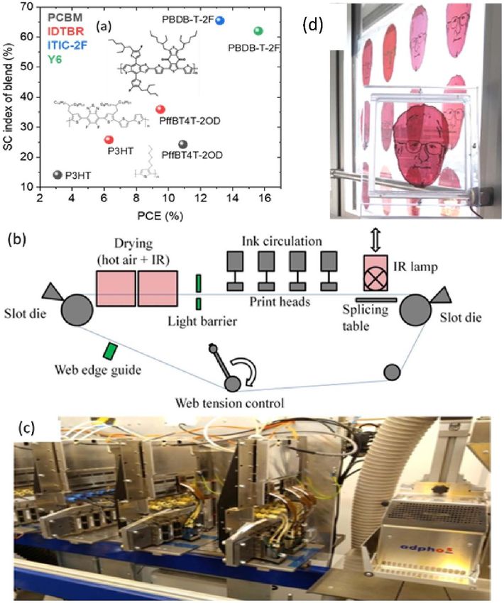
Flex. Print. Electron. 6 (2022) 023001                                                                Y Bonnassieux et al

Introduction                                                      Hussain in section 5. As energy storage is a
                                                              key component to enable untethered electronics,
Ronald Österbacka1, Tse Nga Ng2 and Xiaojun Guo3              section 6 by Cobb and Steingart will discuss energy
1
  Åbo Akademi University                                      storage devices’ requirements and choices for flexible
2
  University of California San Diego                          electronic (FE) systems.
3
  Shanghai Jiao Tong University                                   In section 7 Torsi et al discuss electronic label-free
                                                              detection of biomarkers using water-gated organic
Flexible and printed electronics is a highly mul-             thin-film transistors (TFTs). The generality of the
tidisciplinary research area with the potential for sig-      concept and the promise of single-molecule sensing
nificant breakthroughs in developing new technolo-            combined with manufacturing using printing tech-
gies for ubiquitous electronics.                              nologies open up new avenues for the early detec-
    Flexible and Printed Electronics is a multidiscip-        tion of disease. As discussed by Rivnay in section 8,
linary journal publishing cutting-edge research art-          Bioelectronics and E-textiles by Carmichael et al in
icles on electronics that can be either flexible,             section 9, are promising avenues for integrating elec-
plastic, stretchable, conformable, or printed. In this        tronic devices with the human body, either internally
roadmap, we have collected leading scientists’ views          or externally. These new avenues are still in an early
in various areas related to flexible and printed elec-        phase of development and will experience different
tronics to give their views on the field. From a sci-         challenges over the next years, but with a very bright
entific viewpoint, we wish to outline the present             future.
status, current and future challenges, and what                   For manufacturing, printing tools have steadily
advances in science and technology are required to            progressed to improve feature size resolution, yield,
meet the challenges of flexible and printed electronics       and variability, and the current and future challenges
to become ready for the market.                               are found in the section by Grau and Subramanian.
    The roadmap is divided into three main themes,            Aspects of large-area manufacturing using roll-to-
broadly organized by the main device technologies             roll (R2R) gravure printing of electronic devices are
(sections 1–9), manufacturing (sections 10–12), and           covered by Cho et al in section 11, while in section
systems integration and compact modeling (sections            12 McAlpine et al discuss the possibilities of using
13 and 14).                                                   three-dimensional (3D) printing to integrate elec-
    Organic light-emitting diodes (OLEDs) and                 tronic devices with soft materials into structures with
organic photovoltaics (OPVs) discussed by Peng et al          non-trivial form factors, shapes and functions.
in section 1 and Brabec et al in section 2, respectively,         In the silicon microelectronics industry, device
are probably the most mature of the different devices         compact models, process design kits (PDKs), and a
covered in this roadmap. Both technologies have seen          robust suite of electronic design automation (EDA)
a steady improvement in performance and reduction             tools enable the efficient design of sophisticated cir-
in cost over the past years. Stability without proper         cuits and systems that can be mass-produced by the
encapsulation and high material costs are still a sig-        foundries. In the last decade, research and technology
nificant hurdle when using printing technologies on           development in the FPE field has formed a solid basis
flexible substrates. In section 3, Chabinyc and Patel         for materials, processing, and devices. How to lever-
present organic thermoelectric (TE) materials and             age these technology choices towards making diverse
devices as an emerging energy harvesting technology           functional systems becomes essential. For that, com-
that utilizes heat instead of visible light as a source for   pact models are needed to accurately describe the
energy harvesting.                                            devices’ electrical characteristics and be incorpor-
    Thin film transistors (TFTs) are the workhorse            ated into circuit simulators to perform simulations. A
devices in display industries, and street in section 4        design automation framework to link the FPE tech-
discusses future directions for this area. Meanwhile,         nologies and the commercially available EDA tools
the approach to expand electronic functionalities             to perform system simulation and design verification
through heterogeneous integration of silicon and              is considered the most critical task. Sections 13 and
other crystalline materials on flexible substrates is         14 will discuss the topics of compact modeling and
presented by                                                  design automation, respectively.

                                                 4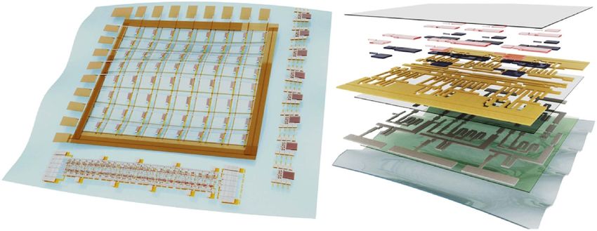
Flex. Print. Electron. 6 (2022) 023001                                                            Y Bonnassieux et al

1. Flexible OLED display and lighting                     Current and future challenges
                                                          Although OLED displays and lighting are already in
Yuguang Ma, Dongge Ma, Junbiao Peng and Yong Cao          the market and developing fast, as shown in figure 2
South China University of Technology                      [8], challenges remain:

Status
OLEDs can be traced back 70 years ago when                High-performance blue EL materials
A Bernanose et al first observed the electrolumines-      Low cost and high-performance organic EL mater-
cence (EL) in organic materials, until 40 years later,    ials still need improvement, especially blue light-
first practical OLED device was built by Tang et al in    emitting materials. At present, high efficiency blue
1987 [1]. Flexible OLEDs have been demonstrated as        phosphorescent materials have operational lifetimes
a promising technique for display and lighting applic-    of only a few 1000 h. Therefore, low-efficiency blue
ations with smart cell phones as the main applica-        light-emitting fluorescent materials are still widely
tion. According to Sigmaintell Consulting, about 470      used in the production of OLEDs. While the TADF
million OLED panels for cell phones (290 million          materials are recognized as potential candidates for
rigid and 180 million flexible) were shipped in           higher efficiencies and longer lifetimes, efficiency
2019, and significantly grew of 5G mobile phones          roll-off at high brightness, as well as the colour pur-
in 2020 from Digitimes Research. Obviously, flexible      ity, still needs to be addressed. There is still signific-
OLEDs would act as an important engine in promot-         ant development needed before materials exhibiting
ing the development of electronic information and         hot-exciton or doublet-radical mechanisms will be
lighting.                                                 applicable.
     The production of an OLED screen is a com-
plex process (the optimal selections of light-
emitting/electronic and hole injection and transport      Simplified OLED device structures
materials, patterning technologies, backplane tech-       Novel device structures are essential to enhance EL
nologies, and encapsulation technologies), with the       efficacy and stability further, as well as to reduce
luminescent material in the core. The emergence of        the costs. To date, complex multilayer structures
novel materials has been pivotal for the development      with high EL performance result in low yields and
of OLEDs, as shown in figure 1. Fluorescent mater-        high costs and simultaneously contribute to the life-
ials show a low internal quantum efficiency (IQE)         time decrease associated with bending resistance in
of 25% [1], whereas the phosphorescent materi-            flexible OLED displays. The enhancement of light
als can achieve 100% IQE [2, 3]. Currently, next-         out-coupling needs to be solved through optical
generation fluorescent organic materials are being        engineering in order to take full advantage of the flex-
rapidly developed, including thermally-assisted-          ible display with folding or even arbitrary stretching
delayed-fluorescence (TADF) [4], hot exciton [5],         (figure 1).
and doublet-radical [6] materials. The progress of
the blue TADF emitters with anexternal quantum
efficiency (EQE) of 20% will greatly promote the          Advanced fabrication technology
display and lighting development. However, these          Owing to the advantages of accurate thickness control
materials are still under investigation and not yet       and flexible multilayer design, vacuum thermal evap-
applied in production lines.                              oration is regarded as an effective method for high-
     At present, flexible OLED displays are mainly fab-   quality film fabrication. Therefore, technologies pro-
ricated via sublimation in a high vacuum system at        ducing high quality, large-area, and patterned films
a high cost, limiting the area. Therefore, solution-      at a low cost that can produce similar quality films
processing has long been anticipated as the manufac-      are required. However, realizing R2R manufacturing
turing technology for future OLED displays.               of print layers with the required degree of accuracy is
     OLEDs will hopefully become the next-                not a trivial task.
generation lighting source due to their unique merits
of environment-friendliness, soft light without glare,
and flexibility, opening up new markets in the auto-      Metal oxide backplane technology
motive, decorative, and medical sectors [7]. Now,         Low temperature poly-silicon TFT (LTPS-TFT), so
OLED lighting technology is steadily improving, and       far, is the main driving backplane of OLED dis-
commercial products with consistent performance           plays. This technology is only suitable for small and
in efficiency, lifetime, and colour quality are appear-   medium-size utilization due to issues with yield.
ing. For example, the efficiency over 220 lm W−1 was      Although metal oxide TFT (such as Indium Gal-
demonstrated in the laboratory in 2020.                   lium Zinc Oxide) [9] has been used to drive OLED

                                             5
Flex. Print. Electron. 6 (2022) 023001                                                                             Y Bonnassieux et al

                             Figure 1. Roadmap of OLED emission materials and flexible OLED displays.

                 Figure 2. Advances and forecast in efficacy, lifetime, and cost of commercial OLED panels over time.

displays with 4K resolution, the electron mobility                  carriers and charge trapping leading to degrada-
and photoelectric stability of the TFTs still need                  tion are well understood and can be analyzed and
improvement.                                                        modeled to find solutions to help to overcome device
                                                                    degradation.
                                                                        To improve the bending resistance while redu-
Advances in science and technology to meet                          cing the cost of flexible OLED displays, a device with
challenges                                                          a planar pn heterojunction structure based on an
The efficiency roll-off of blue EL is envisioned                    interfacial excimer mechanism with EQE over 10%
to be solved by the design of novel aggregation-                    was realized [10]. Besides, the optical design of the
induced delayed fluorescence materials. Alternatively,              encapsulation may significantly improve the device’s
hot exciton materials and high-level charge trans-                  light output efficiency. Furthermore, by design-
fer materials could also provide the solution. Further              ing buffer layers to enhance the adhesion between
understanding and control of charge recombination                   the cathode and organic layer, the bending resist-
and exciton behavior could provide a chance for high-               ance of flexible OLED devices could be significantly
efficiency materials with a narrow emission spec-                   improved. A stretchable OLED device could be real-
trum. The low-charge carrier mobility in disordered                 ized by developing a stable deformable electrode
materials due to the hopping transport of charge                    material.

                                                      6
Flex. Print. Electron. 6 (2022) 023001                                                             Y Bonnassieux et al

                                                               The problems associated with low mobility and
                                                           instability in the backplanes can be solved using rare
                                                           earth elements, such as doped oxide TFTs. Right now,
                                                           the electron mobility of the TFT is over 30 cm2 Vs−1 ,
                                                           and the threshold voltage drift is less than 0.5 V under
                                                           intense white light illumination. This kind of mater-
                                                           ial would be expected to drive large areas and high-
                                                           resolution OLED displays, even for various types of
                                                           printing displays.

                                                           Concluding remarks
                                                           OLED displays and lighting technologies are stead-
                                                           ily improving in efficacy, lifetime, and color quality,
                                                           providing an opportunity for OLEDs in many applic-
                                                           ations. Although the cost of OLED display and light-
                                                           ing products is higher than LCDs and LEDs, which
   Figure 3. A schematic diagram of inkjet printing OLED
   displays.                                               is also a problem to be addressed, some OLED dis-
                                                           play and lighting products are available in affordable
                                                           mobile phones, TV, and automotive lighting applic-
     The inkjet printing technology may solve the bot-     ations. To further improve efficiency, lifetime, and
tleneck problem of low-cost, large-area, and pat-          reducing the cost of OLEDs, based on the deep under-
terning, for manufacturing OLED display and light-         standing of electron excited state processes and carrier
ing, as shown in figure 3. So far, OLED products           transfer/transport process, new light-emitting and
already are commercially produced in the market            matched electron/hole injection and transport mater-
with the currently available inkjet printers and mater-    ials, novel and simple device structures, advanced
ials. Deep understanding ink formulation, droplet jet-     and reliably manufacturing, and efficient TFT driv-
ting and spreading, solvent evaporation, and fusion        ing technologies need innovations. With unremitting
control is conducive to approve mass manufac-              efforts, the full potential of OLEDs as flexible displays
turing OLED panels. To challenge higher tech-              and healthy lighting sources can be unlocked with the
nology, the electrochemical (EC) polymerization            help of printing in the future.
method, which has been successfully demonstrated
as a way of fabricating an OLED display with over          Acknowledgments
1200 pixels, also provides an alternative to pro-
ducing RGB pixels and high-resolution OLED dis-            Funded by the National Natural Science Foundation
plays. For fully utilizing R2R manufacturing, print-       of China (51521002, 22090024) and the Basic and
ing methods for fully printed cathodes should also be      Applied Basic Research Major Program of Guang-
developed.                                                 dong Province (2019B030302007).

                                                    7
Flex. Print. Electron. 6 (2022) 023001                                                                   Y Bonnassieux et al

2. OPVs: technology assessment for
product development

Christoph J Brabec1,2,3, Andreas Distler3 and
Hans-Joachim Egelhaaf 1,3
1
   Friedrich Alexander Universität (FAU), Material
Science, i-MEET,
2
  Forschungszentrum Jülich (FZJ), Helmholtz Institut
Erlangen-Nürnberg (HI-ERN),
3
  ZAE Bayern e.V. Erlangen, Renewable Energies

Status
Photovoltaics (PVs) has become a leading renewable
energy technology. Driven by enormous cost degres-
sion in silicon PVs, electricity from solar energy is
now provided at between 3 and 5 €ct kWh−1 world-
wide. Solar technologies are frequently categorized
into three generations. Mono- or poly-crystalline sil-
icon solar modules are the first generation, thin film
technologies like CdTe, CIGS, etc are the second
generation, while the third generation summarizes
various emerging semiconductors, among them per-
ovskites, quantum dots, dye-sensitizers as well as
organics. OPVs was first implemented in the mar-              Figure 4. Top: visionary concept of the OPV product
ket in 2008/2009 by Konarka, launching a series of            portfolio. Flexible, colourful and semi-transparent modules
                                                              are integrated indoors as well as outdoors into windows,
polymer:fullerene (P3HT:PCBM) based solar mod-                facades, installations, green houses, urban mobility
ules with a nominal peak power between 1 Wp and               concepts or mobile applications and are becoming part of
40 Wp, depending on size. PVs is typically bench-             the daily life, making renewable energies available
                                                              ubiquitously. Bottom: ‘Real World’ integration of OPV
marked in the key performance indicators (KPI) effi-          modules in glass construction elements. Reproduced with
ciency, costs and product lifetime. High performance          permission. (Courtesy Armor SPF GmbH).
modules from the first and second generation are
reaching product module efficiencies of around 20%,
a guaranteed lifetime of more than 25 years and costs
between 0.3 and 0.5 € Wp−1 . OPV modules have a             fulfil requirements to operate applications with power
proven record efficiency of 12.6%, a typical product        requirements reaching from µWs up to MWs.
efficiency of 5%–7%. The first generation of OPV
modules showed lifetimes of up to 10 years under out-       Current and future challenges
door conditions and product costs have come down            Any PV technology must first and foremost meet the
from 10 € Wp−1 and are currently moving towards             classic PV product requirements. Among the clas-
the 1 € Wp−1 regime. Forecasts anticipating the OPV         sical KPIs, efficiency is probably the most advanced.
technology at the GW level are predicting costs as low      The current OPV record efficiency is as high as
as 5 €ct Wp−1 [11]. This is the reason why organic          17.35% on smaller areas and 12.6% on the lab
modules were designed from the beginning of their           module level and already has surpassed the per-
product history to complement the classical PV port-        formance of older technologies like amorphous sil-
folio. Applications such as power plants or roof top        icon (a-Si:H) or dye sensitized solar cells (DSSCs)
integration are of little relevance for OPV as long         [12]. Device lifetime is increasing quickly. By today,
as the technology is still under development. There-        OPV has been proven to be a light stable techno-
fore, applications that are difficult to access for clas-   logy which can operate for tens of thousands of
sical PV technologies are of high relevance (figure 4).     equivalent sun-hours if protected from oxygen and
These make use of product properties such as trans-         humidity [13, 14]. A more serious challenge is the
parency, integrability in surfaces, good indoor per-        development of high performance materials which
formance, negligible temperature coefficients, as well      maintain a low bill of materials (BoM). The BoM
as high flexibility and low weight, but also flexible       of the current flexible OPV technology is domin-
or digital production processes that allow the eco-         ated by the costs for the active material, followed
nomic production of small production quantities or          by packaging costs and electrode costs. Semicon-
single-lot special designs. In summary, a central ele-      ductor costs beyond 100 € gr−1 appear prohibitive
ment of the OPV product roadmap is the design               for mass applications. Few organic semiconductors
of flexible, colourful and semi-transparent products,       (OSCs) like P3HT, PCBM, etc already fulfil these
which can be integrated into existing structures and        requirements, but despite good stability data, their

                                               8
Flex. Print. Electron. 6 (2022) 023001                                                                  Y Bonnassieux et al

efficiency is a factor 3–5 too low for most products.          cost and high quality lamination and packaging pro-
With non-fullerene acceptors (NFAs), which are con-            cesses which operate below 140 ◦ C.
sidered a most promising material class due to their
excellent performance, one must pay more attention             Advances in science and technology to meet
to the costs from the beginning. Vacuum processed              challenges
ultra-barriers as well as inorganic TCO electrodes             The product requirements for OPV materials are
with costs beyond 10 € m−2 need to be replaced                 manifold and include targets for performance, costs,
as well.                                                       stability, toxicity, recycling, colour, etc. That kind
     The most impressive technology feature of OPV             of multi-objective optimization requires a totally
is their production by low temperature and low-cost            different strategy for material optimization, which
solution coating and printing processes, which offers          ideally can be sub-summarized into one figure-of-
highest reliability and throughput for such complex            merit (FoM). Levelized cost of electricity, in its most
architectures as multijunction modules. Neverthe-              simplified version, could be such a FoM, as it takes
less, commercial OPV products fall short in efficiency         into account the lifetime of modules by balancing
compared to record modules processed in the lab                the total costs spent over the total energy produced
(about 5% vs 13%). The consequent reduction of                 within the lifetime span of the module, where r
the responsible loss processes when going from lab             is the discount rate. One recognizes immediately,
to fab requires (a) development of semiconductors              that n, the lifetime of the system, is becoming the
and semiconductor inks which are fully compatible              most influential parameter, which is a major chal-
to environmental and green processing, (b) inter-              lenge for the R&D community, as the assessment
face and charge extraction layers forming long time            of product lifetime and production costs requires at
stable contacts, (c) high resolution patterning pro-           least the operation of a pilot line and years of outdoor
cesses with feature sizes of 100 µm or lower, (d) low          operation.

                              ∑n
                                  Investment Costs (t) [e/a] + Operation Costs (t) [e/a]
                                                                  t
                                                          (1 + r)
                       LCOE = t=1                                     [        ]         .
                                     ∑n
                                         Annual Electricity Generation kWha−1
                                                                          t
                                           t =1
                                                                (1 + r)

One alternative option to standardize such com-                (i-FOM), which was specifically introduced as a
bined efficiency, lifetime and costs consideration             more balanced way to report the relevant per-
for the R&D community is the industrial FOM                    formance of novel material composites [15, 16]

                                    PCE [%] × Stability (T80 [%] , after 200 h, 1 sun, arbitrary T)
                     i − FOM =                                                                      .
                                                                SC

                                                               challenges for OPV and is expected to give valu-
A central element of the i-FOM is the synthetic                able guidance, especially to the current generation
complexity (SC), which balances central mater-                 of NFAs.
ial parameters like complexity, toxicity, purifica-                The current generation of commercial OPV mod-
tion etc which all are decisive for the final costs            ules is processed by slot-die coating with shims, which
[17]. Figure 5(a) shows the SC as cost equivalent              provides lateral resolutions in the mm regime. Laser
as a function of performance for various polymer-              patterning on roll to roll pilot machines already
based semiconductors mixed with four difference                has been proven to reach a down-web resolution of
acceptors. One recognizes that the most efficient              100 µms. In order to be able to produce free patterns
material not necessarily is the most promising                 of solar cells with inconspicuous interconnections,
material for product development. The consequent               digital printing like R2R ink jet printing is envisaged
use of SC and the i-FOM concept is a cent-                     to become the leading production technology [18].
ral strategy to address materials´ related product             Ink jet printing also offers the possibility to print

                                                   9
Flex. Print. Electron. 6 (2022) 023001 Y Bonnassieux et al
Figure 5. (a) SC for three prototype polymer semiconductors blended with four different acceptors, where PCBM is a fullerene
based acceptor and IDTBR, Y6 and ITIC are prototype NFAs. (b), (c) Schematics and image of a loop coater equipped with two
slot die heads and 4 × 4 Samba ink jet heads which can produce OPV modules (d) of any shape and form in a single pass up to
172 mm width at 40 m min−1 . (b)–(d) Reproduced with permission from (P Maisch, PhD Thesis, Erlangen, 2019.).
OPV directly on objects of discretionary shape, which Nevertheless, despite these advantages, OPV has to
provides convenient energy supply for Internet-of- better address the PV KPIs—especially with respect
Things (IOT) applications. to costs and lifetime. To categorize materials in terms
of an integrative KPI, the i-FOM, is proposed to sig-
Concluding remarks nificantly accelerate the OPV technology and product
OPV is rapidly progressing towards a PV technology roadmap.
for dedicated applications, which require exceptional
aesthetics, integrability and flexibility in design. All Acknowledgments
these properties are intrinsic to the OPV technology,
which is colourful and semi-transparent (due to the C J B and H J E gratefully acknowledge funding by
excitonic nature), flexible (due to low temperature the Deutsche Forschungsgemeinschaft (DFG, Ger-
production on flexible substrates) and aesthetic (due man Research Foundation) under the project num-
to future digital printing technologies). This posi- bers 182849149-SFB 953 and INST 90/917, INST
tions OPV as a promising technology for indoor as 90/1093-1, financial support through the ‘Aufbruch
well as outdoor integration on flat as well as curved Bayern’ initiative of the state of Bavaria (EnCN and
surfaces, like glasses, windows, shadings or facades. SFF).
10Flex. Print. Electron. 6 (2022) 023001 Y Bonnassieux et al
3. Organic TE materials and devices Organic TE materials can be integrated into light-
weight modules for use in energy harvesting and local
Michael L Chabinyc1 and Shrayesh N Patel2 temperature control [20]. Importantly, the intrinsic
1
University of California Santa Barbara processability of organic materials permits the fab-
2
Pritzker School of Molecular Engineering, Univer- rication of flexible and conformable TE modules
sity of Chicago based on unique architectures (e.g. corrugated) that
go beyond the rigid, parallel plate configuration. Such
Status architectures enable unique opportunities in imple-
TEs are based on materials that can interconvert mentation such as powering wearable electronics and
thermal and electrical energy [19]. The efficiency of sensors.
this interconversion is related to three properties, the
electrical conductivity (σ), the thermal conductivity Current and future challenges
(κ), and the thermopower (S). The FOM at a given Electrically doped semiconducting polymers must be
2 /
temperature (T) is ZT = σS T κ which is related to resilient to elevated temperatures to push the lim-
the power conversion efficiency of the material. Each its beyond near room temperature applications. The
of these properties is linked to the charge carrier con- stability depends on both the doping method and
centration (n) in a way that makes optimization of polymer itself. For example, polythiophene derivat-
ZT is challenging. In TE modules, it is beneficial to ives with polar side chains of oligo(ethylene oxide)
use two materials where electron conduction (n-type) have shown marked improvements in thermal sta-
dominates in one and hole conduction (p-type) dom- bility in air compared to the nonpolar side chain
inates in the other. equivalent. The stability of dopants can be improved
Semiconducting polymers were suggested as through routes such as ion-exchange of charge trans-
potential TE materials in the 1980s, but only recently fer dopants with more stable counterions [26] and
have significant improvements in performance have new molecular architectures through so-called ‘self-
been obtained due to the advent of new materials doped’ polymers where sidechains are based on ionic
and processing routes [20, 21]. Early research on pendant groups.
polyacetylene revealed that polymers could have TE Currently, n-type polymers do not have the same
performance comparable to inorganic materials [22]. TE performance as p-type polymers. The current best
However, the poor stability of polyacetylene in the n-type organic polymers have PF ≈25 µWm−1 K−2
ambient prevented realization of its promise. The with the highest values from an organometallic
advent of relatively ambient stable conductors, such poly(Ni-ethenetetrathiolate) with ≈450 µWm−1 K−2
as PEDOT:PSS, and the wide range of semiconduct- [20, 27]. The origin of this difference is not well-
ing polymers (e.g. poly(3-alkylthiophenes)) investig- understood given that the electron mobility of many
ated for thin film electronics has greatly improved the polymers and small molecules is within a small factor
ability to develop organic TEs. of the best hole mobilities. It is possible that the dif-
Both p- and n- type organic TE materials have ference is due to a combination of factors such as
been demonstrated using both polymers and molecu- the design of compatible dopants with high mobil-
lar materials (figure 6). The doping process has ity materials, or issues with defects in the materials
proved to be a major step in improving TE proper- because of their stability in ambient conditions. Sur-
ties. An impactful approach has been the sequential prisingly, figure 6 shows that although the absolute
doping method where a dopant infiltrates a neutral performance of n-type material is less than that of p-
polymer with dopant molecules (either from solu- type materials, the power factor at a given electrical
tion or vapor phase) [23]. The improved TE proper- conductivity is higher for n-type polymers.
ties are achieved because the infiltration of the dopant Another factor that is not well-understood is the
into the polymer matrix maintains the crystalline trade-off between electrical conductivity and thermal
order, orientation, and long-range chain connectiv- conductivity in organic materials. The thermal con-
ity permitting high charge carrier mobility. To date, ductivity of insulting polymers is still not easily mod-
the highest reported power factor (σS2 ) for p-type elled due to structural disorder [21]. The anisotropic
polymers is ≈350 µWm−1 K−2 for PEDOT-Toslylate molecular packing in organic materials further makes
and doped selenium-substitute diketopyrrolopyrrole it difficult to relate the thermal and electrical con-
polymers [24, 25]. The ZT of these polymers is ≈0.25 ductivity. Developing new methods that are tailored
based on the thermal conductivities reported in each for the measurement of anisotropic thermal conduct-
with a ZT of >0.5 considered important for practical ivity of OCSs will be needed. Because organic TEs are
applications. very close to practical levels of performance, accur-
11Flex. Print. Electron. 6 (2022) 023001 Y Bonnassieux et al
Figure 6. (a) Seebeck coefficient and (b) power factor of homogeneous semiconducting polymers as a function of the electrical
conductivity for p-type (circles) and n-type (triangles). Data from literature and tables in [19–24].
ate assessment of the thermal conductivity will be a further advances. The ability to spatially tailor trans-
decisive factor in their utility. port properties (i.e. functionally graded materials)
across the length of the organic materials, such as
formation of dopant gradients and microstructure, is
Advances in science and technology to meet potentially simpler than in inorganic materials and
challenges is ripe for exploration [30]. Such an approach can
Improvements in models for charge transport and enable improved distribution of heat when operating
thermopower of OSCs will greatly enhance the abil- TE modules as Peltier coolers.
ity to determine design rules for organic materials.
There has been significant progress developing mod-
els to understand the connection between the ther- Concluding remarks
mopower and the electrical conductivity of homogen- OSCs are close the level of performance that are
eous materials [28]. Strategies to tune the electronic required for practical applications in energy harvest-
density of states (DOSs) in blends towards higher ing and temperature control. Pathways to ZT > 0.5
thermopower have been reported and corroborated seem achievable for p-type polymers and it is likely
experimentally [29]. If such models are coupled with that n-type polymers can also achieve similar or
similar advances in models for thermal transport, it even higher performance. If new materials pairs that
will accelerate the ability to improve the performance are readily processable are developed, then we can
of materials. expect to see greater exploration in module designs
New architectures for TE modules that leverage that leverage the unique properties of semiconduct-
the unique features of OSCs, such as their ability ing polymers.
to be printed or extruded by additive manufactur-
ing (AM) methods, will provide a pathway to real- Acknowledgments
ize their performance [20]. Coupling designs of mod-
ules that leverage the anisotropies in the electronic M L C acknowledges support from NSF DMR
and thermal conduction of polymers could provide 1808622.
12Flex. Print. Electron. 6 (2022) 023001 Y Bonnassieux et al
4. Printed or flexible TFTs; materials and manufacturing production, although there is early
performance stage manufacturing of non-printed organic TFTs.
Technology adoption is held back by issues of uni-
Robert A Street formity and process integration as well as device per-
Palo Alto Research Center formance limitations of mobility and speed as com-
pared to inorganic TFTs. Many of the TFTs shown in
Status figure 7 are made with Si/SiO2 gate dielectric but have
OSCs dominate research on printed TFTs and lower mobility when made with a solution-deposited
since 1985 their mobility has increased from dielectric on a flexible substrate.
10−5 cm2 Vs−1 to about 10 cm2 Vs−1 (see figure 7) Printed TFTs have the additional challenges of
[31, 32]. The improvement resulted from the dis- print resolution, parasitic capacitance and process
covery of new OSCs, particularly the donor–acceptor integration. Ink-jet printing is an attractive method
polymers. Small molecules tend to have higher mobil- because it is a digital technology. However, com-
ity than polymers, although many cannot be depos- mercial ink-jet printers have a printed feature size
ited from solution. The mobility and other TFT char- of 40–50 µm, while large area lithography has fea-
acteristics depend on the choice of gate dielectric and ture size down to 1–3 µm. Comparable printed fea-
the method of fabrication. Organic TFTs are readily tures are possible but not yet with high throughput
made flexible by deposition on a wide range of plastic scalable commercial systems [38]. Large TFTs take
substrates. Instability to a gate bias voltage and ambi- up space and have high parasitic capacitance, which
ent humidity was a constant issue with organic TFTs, reduces circuit performance compared to lithograph-
but has substantially improved [33]. ically defined devices. The challenge is to reduce the
Flexible inorganic TFTs are in production for disparity in feature size to make printed TFTs compet-
liquid crystal displays, organic light emitting dis- itive with lithography. Printing systems must print all
plays and x-ray detectors—amorphous silicon (a-Si), the various materials used in the TFT and obtaining a
LTPS made by laser recrystallization and metal oxides, thin uniform defect-free gate dielectric is particularly
primarily InGaZnO (IGZO). Backplanes are fabric- challenging.
ated on a thin polyimide film released from a glass Hybrid circuits (figure 8) are developed to solve
carrier after processing, giving equivalent TFT per- some of the performance limitations [39]. Printed
formance to those deposited on glass. A-Si and IGZO devices provide the simple circuit elements and sil-
can be deposited below 200 ◦ C with minor reduc- icon integrated circuits (ICs) provide the capabil-
tion in performance making them accessible to other ity for complex processing, data storage and wireless
plastic substrates [34], and IGZO can be printed from communication. The problem is that the IC could
a sol-gel solution with annealing at about 400 ◦ C. contain virtually all the necessary devices so that few
IGZO flexible microprocessors have been demon- printed TFTs are needed. The challenge for TFT tech-
strated [35]. nology is to be capable of sufficiently complex cir-
Printed and flexible TFT materials outside the cuits that minimize and eventually remove the need
above categories include the perovskites developed for ICs. The challenge for ICs is to be thin, flexible
for solar cells, carbon nanotubes (CNT), graphene and bondable to plastic substrates.
and other two-dimensional (2D) materials, each of Inherently large circuits such as displays, and
which show promising TFT properties [36]. Electro- devices such as TFT sensors, high voltage or ferro-
lyte gated and EC TFTs use a liquid or solid electro- electric TFTs, as well as other characteristics such as
lyte gate dielectric and operate by transferring charge stretchability or transparency, may provide oppor-
from the gate dielectric directly to the semiconductor, tunities that only printed or FEs can meet. The chal-
often PEDOT. ECTFTs typically have high current lenge is to find applications of this type and to develop
but slow response and have applications for chemical new devices to satisfy the need.
sensing [37].
Printed TFTs are largely targeted at IoT devices,
Advances in science and technology to meet
small and possibly disposable flexible tags with
challenges
an internet link. Such applications could increase
The ideal printed or flexible TFT has high mobility,
enormously if advanced by a robust printing and
high on/off ratio, sharp turn-on, small features with
TFT material technology. Concerns about stabil-
precise dimensions, is self-aligned with a high k gate
ity and process integration have so far prevented
dielectric, and is stable against electrical stress and
printed TFTs from reaching the display backplane
ambient exposure. There is broad scope for contin-
market.
ued development of materials to achieve these goals.
Continued improvement in OSCs with higher mobil-
Current and future challenges ity and increased stability against ambient exposure
Numerous printed organic TFT device prototypes and bias stress is a reasonable expectation. Devel-
are reported but have not yet reached significant opment of printable metal oxides including p-type
13Flex. Print. Electron. 6 (2022) 023001 Y Bonnassieux et al
materials is to find the combination of semiconductor
and gate dielectric that give high performance.
The printing process needs further research to
achieve higher density devices with faster circuit
speed, both of which are limited by printer resolution
and precision. Printed feature size should decrease
to 5 µm or below in high throughput systems, and
feature overlaps to 2 µm with corresponding align-
ment accuracy between layers. Self-aligned processes
are desired as the parasitic TFT capacitance limits the
circuit frequency. There are printing techniques that
are capable of high resolution, such as gravure, extru-
sion and nano-imprint technology, but need further
research to demonstrate process integration of the
TFT devices and circuits. Printers should be enabled
for the multiple materials that are used in devices. As
feature sizes reduce, the problems of the liquid/sur-
face interactions increase and will need more research
Figure 7. Organic TFT mobility trend over 3 decades,
showing the typical range of values for p-type and n-type into wetting, inter-diffusion and other surface inter-
devices [31]. actions. Since printed TFTs will have limited resol-
ution for the foreseeable future, 3D integration can
help achieve high density circuits. Initial progress in
3D integration needs to be developed into a robust
technology [40].
Vacuum deposited and lithographically patterned
flexible a-Si, LTPS and oxide TFTs are in volume pro-
duction and so their research advances are directed
to new application spaces. Oxide TFTs are limited in
their use for backplane drivers by the lack of good
p-type materials for complementary circuits, which
is an important gap to fill.
Figure 8. Printed light and temperature wireless sensor, as
an example of hybrid flexible electronics, with some printed
TFT circuits, some conventional components and printed Concluding remarks
silver interconnects. © [2017] IEEE. Reprinted, with Printed TFTs have progressed greatly but still fall
permission, from [39]. short of being a robust manufacturing technology.
There is a wide variety of materials, devices, circuits
and processing approaches that have been demon-
materials, that can be processed at low temperature strated at the prototype stage for printed and/or flex-
with stability and high mobility would open up new ible systems. Future research and development will
device opportunities. Novel TFT materials including determine which of these approaches come together
graphene, CNT and transition metal dichalcogenides, to form a successful manufacturing ecosystem, cap-
show promise but need research to develop them into able of addressing novel applications and competing
robust printed TFT technologies. Important for these with conventional approaches.
14Flex. Print. Electron. 6 (2022) 023001 Y Bonnassieux et al
5. Flexible silicon electronics the general area of FE [43]. The concept is to con-
tinue using traditionally rigid ICs because they are
Muhammad M Hussain small, readily available, and cheap. In reality, none
KAUST and UC Berkeley of these is entirely true. Additionally, it is contradict-
ory to the vision of a fully FE system. But, why do
Status we even need a fully FE system? To address this, as
FEs is an emerging area which potentially will oblit- an example, one of the most prized objectives for the
erate the interfacing barrier between readily available FE community is to develop an implantable brain–
physically rigid electronic components and natural machine interface that can be placed in the intra-
biology which have asymmetric surfaces, irregular cranial space on soft matters of the human brain to
architecture, soft and textured ‘components’. Such maximize its interaction. The concept expands fur-
electronics will allow us to interface seamlessly with ther that such a system will be able to transmit data
natural biology (human, animals, plants, etc.). That even when the scalp is closed. However, not a single
will help us to understand natural phenomena deeply demonstration as of today eliminates the necessity of
and to reapply them in our daily life through nature- the physically rigid data management ICs [44, 45].
inspired engineering. Since 2000, substantial pro- On occasions, it has been recommended to use serial
gress has been made in the general area of FEs [41]. ports to interface between the sensor array and the
This drive is influenced by innovation in materi- accessorial I/O interfacial electronics. The question
als. Since polymers are naturally flexible there has is why these challenges still exist? The truth is lack
been noteworthy attention toward polymer-based of appetite to use physically rigid traditional elec-
electronics. In parallel, 1-dimensional (1D) materials tronic materials due to their lack of novelty in curi-
(such as CNTs and nanowires), as well as 2D mater- osity driven academic research has made it a show
ials (such as graphene and two dimensional dichal- stopper to begin with. Next, the complexity related
cogenide materials) are all ultra-thin and thus, nat- to their processing using complementary metal oxide
urally flexible. Another approach has been to use semiconductor (CMOS) has been left with semicon-
zero-dimensional materials (organic materials) and ductor industries who sporadically showed its prom-
some of the aforementioned materials as ‘ink’ in ise but due to absence of clearly profiting ventures
inkjet-printed texturing and/or 3D printed shaping. never picked it up seriously. Additionally, absence
Undoubtedly, major progress has been made in using of sophisticated equipment in the academic environ-
these materials for FEs. Nonetheless, one critical chal- ment also played a negative role. To achieve a fully
lenge remains unaddressed. Although the aforemen- FE system even with only the data management elec-
tioned materials show exciting potential for a variety tronics as flexible silicon electronics, major obstacles
of applications, for data management their efficacy have to be overcome: thinning down the silicon-based
remains questionable and not competitive to exist- bare die containing the transistors and other electron
ing traditional electronic materials such as mono- devices; their reliable transfer to the soft encapsula-
crystalline silicon which is used to make 90% of tion materials; placement and attachment; intercon-
the electronics today [42]. Before we proceed, let us nection, etc are a few to name. While some demon-
first address what is data management. Data man- strations address a few of these, rarely all have been
agement includes data processing, data storage and addressed in a comprehensive manner.
data transmission. Since any electronic system focus-
ing on the IoT or Internet of Everything involves
Advances in science and technology to meet
sensors, it is obvious that gathered data through the
challenges
sensors has to be managed properly. Although widely
Initially, silicon-on-insulator (SOI) substrates were
used crystalline thin films like silicon, silicon ger-
used to remove the buffer oxide layer conveniently to
manium, germanium, III–V, gallium nitride, silicon
release the top SOI layer for FE materials. However,
carbide, etc are essential today for data management
some critical show stoppers nearly halted its progress:
electronics (such as logic microprocessor, memory
expense and lack of proper device isolation strategy
and transceiver), optoelectronics, power electronics,
for ultra-thin (3–150 nm) flexible SOI layer [42].
etc, they are physically rigid and brittle. Therefore,
Another approach capitalized on using silicon (111)
nearly no attention was paid to these materials irre-
substrate is due to higher atomic density, it is diffi-
spective of their reliability, manufacturability, and
cult to etch crystalline plane (111) while it is relatively
functionality. The idea has been to use them as they
easy to etch vertical plane (100). Unfortunately, due
are but that contradicts the vision of a fully FE
to high defect density, (111) plane is not recommen-
system.
ded for any data management electron device [42].
Next approach has been to create a porous network in
Current and future challenges bulk silicon substrate using anodic etching followed
Today, flexible hybrid electronics (FHE) is a pop- by expensive epitaxial growth of silicon before peel-
ular term in the scholarly community working in ing it off using the already formed porosity. Expense
15Flex. Print. Electron. 6 (2022) 023001 Y Bonnassieux et al
Figure 9. In this schematic (left to right and top to bottom), a highly manufacturable heterogeneous integration strategy is
demonstrated for achieving a flexible silicon electronic system. Initially a soft material temporary host site is adopted followed by
polyimide deposition. Next patterning is done where each pattern is curved in a way to match the shape and size of the incoming
flexible silicon ICs. Then, an interconnect metal layer is deposited followed by patterning. On separate locations, logic/memory,
radio frequency (RF) IC and battery are curved with certain shapes and sizes to provide them with some unique identities. Then
they are transferred to the temporary host sites and their placement (dubbed as Lego like Pick and Place Assembly) is done (like
DNA assembly, each component will fit only in designated location due to the curved pattern in the host site and the unique
identities formed in the ICs). Polydimethylsiloxane (PDMS) is formed and etched back to reduce its thickness much lower than
the ICs. ICs are now etched back with reactive ion etching (RIE). Next another layer of PDMS is formed with patterning to reach
out to the underlying thinned downed ICs. Metal layer is deposited followed by patterning to curve out antennas and free space
for placing the solar cells facing upward. Another layer of PDMS is formed and patterned to conduct corrugation enabling etching
to curve an alternate pattern in the solar cells to make them flexible. Release the flexible system from the temporary host site, flip
it to expose the sensors with the data management electronics and battery embedded in the middle of the soft encapsulation layers
(placing them in the neutral plane) while exposing the antenna and the solar cells on the other side of this coin like 3D
architecture. (M M Hussain and S F Shaikh, ‘HETEROGENOUS INTEGRATION OF PLURAL GRAPHENE SENSORS ON 3D
COIN CMOS ELECTRONICS,’ PCT/IB2020/051141, 2019.).
physically damaging, it also has limited removal abil-
ity, leaving the left over silicon not reasonably flex-
ible. Also, some of the processes are expensive spe-
cially considering they remove a significant portion
of the substrates. This ultimately compromises device
performance such as PV efficiency of crystalline sil-
icon solar cells [42]. Finally, controlled cracking in
the substrate using a metallic layer has been demon-
strated which suffers from the loss of any free hanging
micro-electro-mechanical systems (MEMS) devices
in the back end of line processes. Additionally they
are complex and expensive [42]. Since, none of these
processes has shown a full blown pragmatic prospect,
Figure 10. A fully flexible standalone integrated silicon only three entities have made substantial progress.
electronic system with microprocessor, memory, BLE Belgium based imec has shown a variety of encapsu-
transceiver, antenna, an array of micro lithium ion
batteries, solar cells and sensors with light actuator.
lation techniques for ultra-thin silicon but they have
never been able to demonstrate a full system [46].
USA based American Semiconductor sells some use-
ful chips like microprocessors and analog-to-digital
and low throughput have obstructed its progress [42]. converter, but again they also have not shown a full
Another approach has been to use abrasive back system [47]. We are the only group who have shown
grinding or lapping/polishing to reduce the material a 3D architecture for fully functioning physically flex-
from the back side of silicon substrate. Not only it is ible standalone electronic system integrating sensors,
16Flex. Print. Electron. 6 (2022) 023001 Y Bonnassieux et al
actuators, power supply/storage and data manage- ally using electronics in their products due to their
ment electronics (figures 9 and 10) [48–50]. existing rigidity and bulkiness. Finally, comprehens-
ive analytical studies need to be conducted to validate
each material and process to ensure that the perceived
Concluding remarks FEs will not compromise the advantages offered by
As much as FEs offer exciting promise, unless we their rigid counterparts. For absolutely novel wear-
have heterogeneous integration strategies of hybrid able and implantable applications, it will be critical
sets of materials to develop manufacturing grade to retain their performance and reliability in context
fully flexible standalone electronic systems, its prom- of uncertainty posed by user behavior.
ising potential will not be fully realized. Adopt-
ing some generic integration sequence, as we have Acknowledgments
developed and demonstrated, will allow the user and
the developer community to project some highly The author acknowledge many students, post docs
profiting applications for immediate use by con- and research staffs who have worked on projects
sumers. Also, some niche areas need to be identi- involving FEs. The authors also acknowledge a vari-
fied focusing on industries who are not tradition- ety of funding sources.
17You can also read