Rubbery computing - TU Dresden
←
→
Page content transcription
If your browser does not render page correctly, please read the page content below
Rubbery computing
               Katherine E. Wilsona , E.-F. Markus Henkea,b , Geoffrey A. Slipherc , and Iain A. Andersona,d,e
                  a
                    Biomimetics Lab, Auckland Bioengineering Institute, University of Auckland, Level 6, 70
                                           Symonds Street, Auckland 1010, New Zealand
                             b
                               Institute of Solid-State Electronics, TU Dresden, Dresden, Germany
                     c
                       U.S. Army Research Laboratory, 2800 Powder Mill Road, Adelphi, MD 20783, USA
                                   d
                                     StretchSense Ltd, 27 Walls Road, Auckland, New Zealand
                  e
                    Engineering Science, University of Auckland, 70 Symonds Street, Auckland, New Zealand

                                                                           ABSTRACT
               Electromechanically coupled dielectric elastomer actuators (DEAs) and dielectric elastomer switches (DESs)
               may form digital logic circuitry made entirely of soft and flexible materials. The expansion in planar area of a
               DEA exerts force across a DES, which is a soft electrode with strain-dependent resistivity. When compressed,
               the DES drops steeply in resistance and changes state from non-conducting to conducting. Logic operators may
               be achieved with different arrangements of interacting DE actuators and switches. We demonstrate combinato-
               rial logic elements, including the fundamental Boolean logic gates, as well as sequential logic elements, including
               latches and flip-flops. With both data storage and signal processing abilities, the necessary calculating compo-
               nents of a soft computer are available. A noteworthy advantage of a soft computer with mechanosensitive DESs
               is the potential for responding to environmental strains while locally processing information and generating a
               reaction, like a muscle reflex.
               Keywords: Artificial muscles, Dielectric elastomer switch, Logic circuits

                                                                    1. INTRODUCTION
               Computing circuitry with standard electronics are typically hard components mounted on rigid printed circuit
               boards. A challenge then for controlling soft robotics is developing materially softer control elements. Instead
               of mismatching clunky electronics with soft structures, comparably soft and flexible electronics may provide
               integrated intelligence for soft robots. Smart soft robots would not be dependent on external electronic modules
               nor be burdened by on-board hard electronics.
                   A favoured actuator technology in soft robotics is the dielectric elastomer actuator (DEA), also known as
               an artificial muscle. The DEA structure is a dielectric membrane between two compliant electrodes. Applying
               voltage to the electrodes induces elctrostatic forces known as Maxwell pressure, which squeezes the membrane in
               thickness and expands the area.1, 2 DE artificial muscles can generate large strains and have properties similar
               to those of biological muscle, including power density, pressure, and strain-actuation.3–6
                   The dielectric elastomer switch (DES), introduced by O’Brien et al. in 2010,7 enables intelligent control of
               artificial muscles, without the need for conventional electronics. The DES is a flexible piezoresistive electrode
               that can turn charge on and off with stretch. Coupling DESs with artificial muscles produced several systems
               of note including a ring oscillator,8 self-commutating motor,9 and generator.10
                   DESs may directly couple mechanical strain with digital logic.7, 11 It was recently demonstrated that simple
               arrangements of DEA and DES can form combinatorial circuits, i.e. the fundamental Boolean logic gates.12
               Benefits of these designs include that only soft polymer and carbon materials are needed and the gating mecha-
               nism relies on mechanical strain rather than standard electronics. Logic elements made from soft materials allow
               signal processing to be integrated with artificial muscle devices, and mechanical feedback from the system may
                   Further author information: (Send correspondence to K.E.W.)
                   E-mail: kwil803@aucklanduni.ac.nz

                               Electroactive Polymer Actuators and Devices (EAPAD) 2017, edited by Yoseph Bar-Cohen, Proc. of SPIE
                                    Vol. 10163, 101632H · © 2017 SPIE · CCC code: 0277-786X/17/$18 · doi: 10.1117/12.2260393

                                                                   Proc. of SPIE Vol. 10163 101632H-1

Downloaded From: http://proceedings.spiedigitallibrary.org/ on 05/11/2017 Terms of Use: http://spiedigitallibrary.org/ss/termsofuse.aspx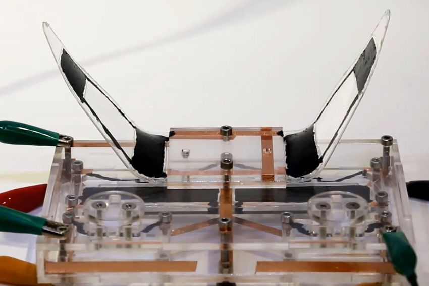
be directly coupled to the circuitry. The capabilities of such circuits may be expanded by developing memory
               elements or sequential circuitry.
                  Sequential logic circuits have memory function and can store data. Multiple components can make up
               higher order functions such as counters and registers. Memory functions can expand the intelligence of soft
               robotics devices, allowing feedback and learning ability to be incorporated. Artificial muscle circuits may be
               an alternative to hard and heavy conventional electronics for control of soft robots, enabling smart entirely soft
               robots.

                                                         2. MATERIALS AND METHODS
               DEAs were fabricated by sandwiching VHB 4905 (3M) between two painted-on carbon grease electrodes, Nyo-
               gel 756G (Nye Lubricants). The membrane was equibiaxially pre-strained approximately 362%. DESs7 were
               composed of a mixture of 5:1 Molykote 44 Medium grease to Cabot Vulcan XC72 carbon black. Switch tracks
               were transfer printed onto membranes using a PDMS stamp. Switch horizontal tracks were pre-strained ap-
               proximately 200% so that the switch was non-conducting at rest and became conducting when the pre-strained
               tracks were compressed. Membranes holding DEAs and DESs were mounted on rigid acrylic (Perspex) frames.
                  Logic circuit components were composed of one or more pairs of a DEA and DES. One pair or unit is shown
               in Figure 1. A 3mm-wide strip of Perspex was placed between the actuator and switch to promote uniform
               deformation of the switch when the actuator expanded. Metal screws and copper tape in the corners of the
               frame provided electrical connections to a high voltage (HV) source. Logic circuits include 50 MΩ pull-up or
               pull-down resistors, which inhibited spark erosion of the switches.
                  Input voltages were 0kV or 3kV corresponding to logical low (0) and high (1) values, respectively. For output
               values, the low logic state was considered to be voltages less than 1kV and the high logic state was voltages
               greater than 2.5kV. Measurements were taken with LabView.

                                                                              Perspex frame

                                                                                   DEA

                                                                               Perspex strip

                                                                                    DES

               Figure 1. Schematic (left) and picture (right) of a circuit structural unit - a paired DEA and DES mounted on a
               transparent Perspex frame with an extra 3mm-wide Perspex strip placed between the actuator and switch. Applying
               voltage to the DEA induced in-plane expansion, which compressed the DES.

                                                                3. DE LOGIC CIRCUITS
               Building blocks for combinatorial logic circuits are Boolean logic gates, including NOT, NAND, AND, NOR,
               OR, XNOR, and XOR gates.13–15 The NOT gate is also known as an inverter. It has one input and one
               output. When the input is low the output is high, and conversely the output is low when the input is high.
               The other six logic gates have multiple inputs. Table 1 below shows the truth tables for two-input gates.
               Example configurations of the fundamental Boolean logic gates were demonstrated previously.12 Combinatorial
               logic circuits enable information processing. Thus DE logic gates may implement various functions or “decision
               making” abilities in artificial muscle devices. A demonstrative device which functions with NAND gate control
               is presented below in section 4.

                                                                   Proc. of SPIE Vol. 10163 101632H-2

Downloaded From: http://proceedings.spiedigitallibrary.org/ on 05/11/2017 Terms of Use: http://spiedigitallibrary.org/ss/termsofuse.aspx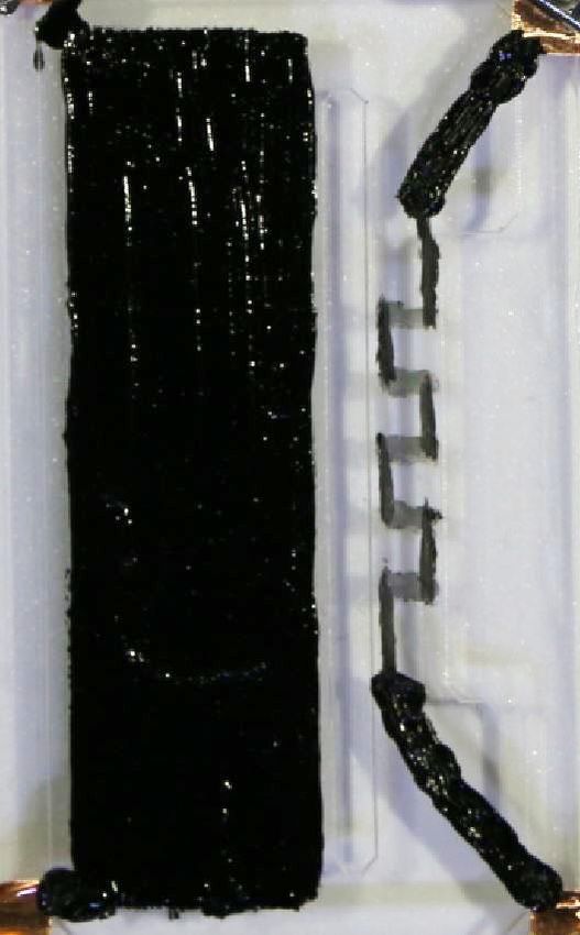
Table 1. Truth table for 2-input Boolean logic gates.

                                                  Inputs                                Output
                                                   1 2       NAND          AND         NOR OR         XNOR        XOR
                                                   0    0        1             0        1       0         1         0
                                                   0    1        1             0        0       1         0         1
                                                   1    0        1             0        0       1         0         1
                                                   1    1        0             1        0       1         1         0

                   DE muscles and switches can also compose sequential logic circuitry. Basic components of sequential logic
               circuitry are latches and flip-flops. Latches are asynchronous, or driven by events, and flip-flops are enabled by
               a clock signal. Both latches and flip-flops remember their state and can be used to store data. Some common
               memory elements which we demonstrate here include set-reset (SR) latch, modified SR latch, and D flip-flop.
                   The SR latch is a 2-input logical operator that remembers its previous state and only changes state when
               one of the inputs changes value from low to high. The SR latch can be formed from combinations of Boolean
               logic gates. Here we used NOR gates as shown in Figure 2. The output Q is set high when input S is high, and
               Q is reset low when input R is high. The latch remembers its state and does not change if both S and R remain
               low. Driving both inputs high is an invalid state and the latch will lose functionality.

                                                                     Table 2. SR Latch truth table.

                                                                           S       R        Q
                                                                           0       0   no change
                                                                           0       1        0
                                                                           1       0        1
                                                                           1       1    invalid

                                                                     Proc. of SPIE Vol. 10163 101632H-3

Downloaded From: http://proceedings.spiedigitallibrary.org/ on 05/11/2017 Terms of Use: http://spiedigitallibrary.org/ss/termsofuse.aspx
V1

                                                                                                       Vout
                                                                                                                            S
                                                                                                       +HV
                                                                                               50 MΩ
                                               V2

                                                                                                                                                        Q
                                             GND                                                                           R
                                            (a) NOR gate schematic. +HV is                                           (b) SR latch circuit di-
                                            3kV. V 1 and V 2 are input voltages.                                     agram, includes 2 NOR
                                                                                                                     gates. The two inputs are
                                                                                                                     labelled S and R, and the
                                                                                                                     output is labelled Q.

                                                                       4
                                                      Output voltage

                                                                                                                                          Logic state
                                                                       3
                                                         Q (kV)

                                                                                                                                      1
                                                                       2
                                                                       1                                                              0
                                                                       0
                                                                       4
                                                      Input voltage

                                                                                                                                          Logic state
                                                                       3
                                                         S (kV)

                                                                                                                                      1
                                                                       2
                                                                       1                                                              0
                                                                       0
                                                                       4
                                                      Input voltage

                                                                                                                                          Logic state

                                                                       3
                                                         R (kV)

                                                                                                                                      1
                                                                       2
                                                                       1                                                              0
                                                                       0
                                                                           0   10    20   30    40   50   60 70 80   90 100 110 120 130
                                                                                                          Time (s)

                                                                               (c) SR latch voltage response graph.

                                                                       Figure 2. SR latch design and operation.

                   From the voltage response graphs (Figures 2(c)), it can be seen that to set or reset the latch only a pulse
               at either input is necessary, i.e. Q will stay in its new state after the pulse ends. The pulse duration necessary
               to set or reset the latch is determined by the time delay through the circuit. Due to the viscoelasticity of the
               VHB membranes,16 compression of a DES may be delayed because viscous losses in the membrane oppose the
               elastic deformation. This results in delayed switching and consequently a gradual instead of sharp change in
               output voltage. This is evident at falling edges of the output voltage. As structures are hand-made, there is
               high sample-to-sample variability. For a single unit, a typical switching response time, i.e. from input signal
               actuating a muscle to output signal changing logic state, was approximately 2.5 seconds.12
                   The S̄R̄ latch, also referred to as the modified SR latch or not SR latch, is essentially an inversion of the SR
               latch. Figure 3 shows the configuration made up of 2 NAND gates. Output Q is set high when input S̄ is low,
               and Q is reset low when input R̄ is low. The latch remembers its state and does not change if both S̄ and R̄
               remain high. Driving both inputs low is an invalid state and the latch will lose functionality.

                                                                                    Proc. of SPIE Vol. 10163 101632H-4

Downloaded From: http://proceedings.spiedigitallibrary.org/ on 05/11/2017 Terms of Use: http://spiedigitallibrary.org/ss/termsofuse.aspx
Table 3. Modified SR latch truth table.

                                                                                           S̄   R̄            Q
                                                                                           0    0         invalid
                                                                                           0    1             1
                                                                                           1    0             0
                                                                                           1    1       no change

                                                +HV
                                                                                   50 MΩ
                                                                                                Vout
                                                  V1

                                                                                                                      S̄
                                                                                                                                                      Q

                                                  V2

                                                GND                                                                   R̄
                                                (a) NAND gate schematic.                                      (b) S̄R̄ latch circuit dia-
                                                +HV is 3kV. V 1 and V 2 are                                   gram, includes 2 NAND
                                                input voltages.                                               gates. The two inputs are
                                                                                                              labelled S̄ and R̄, and the
                                                                                                              output is labelled Q.

                                                                        4
                                                       Output voltage

                                                                                                                                        Logic state

                                                                        3
                                                          Q (kV)

                                                                                                                                    1
                                                                        2
                                                                        1                                                           0
                                                                        0
                                                                        4
                                                       Input voltage

                                                                                                                                        Logic state

                                                                        3
                                                          S̄ (kV)

                                                                                                                                    1
                                                                        2
                                                                        1                                                           0
                                                                        0
                                                                        4
                                                       Input voltage

                                                                                                                                        Logic state

                                                                        3
                                                          R̄ (kV)

                                                                                                                                    1
                                                                        2
                                                                        1                                                           0
                                                                        0
                                                                            0      20      40   60       80     100   120   140   160
                                                                                                       Time (s)

                                                                                 (c) S̄R̄ latch voltage response graph.

                                                        Figure 3. Modified SR latch design and operation.

                                                                                   Proc. of SPIE Vol. 10163 101632H-5

Downloaded From: http://proceedings.spiedigitallibrary.org/ on 05/11/2017 Terms of Use: http://spiedigitallibrary.org/ss/termsofuse.aspx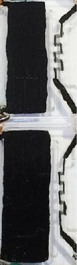
The D flip-flop includes a clock signal and one other input labelled D. Here we used a configuration made
up of 4 NAND gates as shown in Figure 4. The D flip-flop may change state when the clock signal is high, and
the input is shifted to the output at the next clock signal (Qt+1 = Dt ).
Table 4. D flip-flop truth table.
CLK D Q
0 0 no change
0 1 no change
1 0 0
1 1 1
D
Q
CLK
(a) D flip-flop circuit diagram, includes 4 NAND
gates. Inputs are labelled D and CLK. Output is
labelled Q.
e 4
Output voltage
Logic state
3
korli41411 1
(kV)
2
1 0
0
4
Input voltage
Logic state
3
D (kV)
1
2
1 0
0
4
Timing signal
Logic state
CLK (kV)
3
1
2
1 0
0
0 20 40 60 80 100 120 140 160 180 200
Time (s)
'"\-
(b) D flip-flop image. (c) D flip-flop voltage response graph.
41" Figure 4. D flip-flop design and operation.
It is noteworthy that other circuit configurations are possible, and other common circuit components may
be constructed such as JK and T flip-flops. Results support that both combinatorial and sequential circuit
1111111
components are available using HV DE switching. Therefore, higher order functions such as counters and
registers can be formed from combining multiple elements. For example, a n-bit shift register may be formed
from n number of D flip-flops. Complex networks may need to take into account the latency period due to
viscoelastic properites of the DE membrane.
Proc. of SPIE Vol. 10163 101632H-6
Downloaded From: http://proceedings.spiedigitallibrary.org/ on 05/11/2017 Terms of Use: http://spiedigitallibrary.org/ss/termsofuse.aspx
Current structures have limited lifetime and reliability. Improved properties may be achieved with materials
other than VHB and carbon grease. Silicone, for example, may provide faster response time and experience
significantly less creep than the VHB membranes used here.17 Also, the switch material is susceptible to spark
erosion at high voltage. Enhanced switches may have greater electrical breakdown strength and sharper switch-
ing characteristics. Furthermore, an automated fabrication process would reduce sample-to-sample variability
and improve production quality.
4. DRIVING DE ARTIFICIAL MUSCLE ROBOTS
The DE logic circuits described above provide high voltage control for DE robots. In this section, we demonstrate
some DE devices which are driven by artificial muscle circuitry. Examples include a safety switch gripper and
biomimetic dragonfly.
A safety switch gripper was made to demonstrate simple control with a NAND gate (design schematic was
shown in Figure 3(a)). The device is modelled after two-hand controls, which are used to avoid injury of the
machine operators by keeping their hands away from the point of operation. The structure contains two button
switches that provide the input data. Each button is a DES which is conducting at rest and becomes non-
conducting when the button is pressed. Grippers move - open or close - in response to the NAND gate output
value. The grippers contain DEA windows framed by 250 micron thick PET. A low signal to the grippers leaves
the DEA relaxed so that the elastic restoring force makes the grippers close. A high signal expands the DEA
and makes the grippers unfold or open. The grippers remain open until both buttons are pressed, i.e. when
both inputs to the NAND gate are 1, the output is 0, which makes the grippers close.
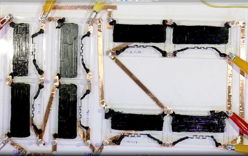
Images of the NAND gate during operation at each of the input states is shown in Figure 5. It can be
observed that a low input (0) leaves the corresponding switch relaxed and a high input (1) compresses the
switch. Refer to Table 1 for NAND gate logic. Figure 6 shows the action states of the gripper device that
correspond to the different NAND gate states.
Inputs
0,0 0,1 1,0 1,1
r
ç'
ç
Figure 5. Images showing the states of operation of the NAND gate during the four possible input combinations. Refer
to Table 1 for the logic truth table. Low input (0) leaves the DEA and DES relaxed. High input (1) expands the DEA
and consequently compresses the DES.
Proc. of SPIE Vol. 10163 101632H-7
Downloaded From: http://proceedings.spiedigitallibrary.org/ on 05/11/2017 Terms of Use: http://spiedigitallibrary.org/ss/termsofuse.aspx(a) Neither button is pressed. Inputs to the (b) One button is pressed. Inputs to the NAND
NAND gate are 0 and 0, so the output is 1. gate are 0 and 1, so the output is 1. The gripper
The gripper DEAs are actuated, making the grips DEAs are actuated, making the grips open.
open.
(c) One button is pressed. Inputs to the NAND (d) Neither button is pressed. Inputs to the
gate are 1 and 0, so the output is 1. The gripper NAND gate are 1 and 1, so the output is 0. The
DEAs are actuated, making the grips open. gripper DEAs are relaxed, making the grips close.
Figure 6. Images of the safety switch gripper during operation.
Another demonstrative device is a biomimetic dragonfly. The robot has two wings which flap 180 degrees
and are driven by an oscillator. The oscillator is composed of 3 inverters in a closed loop (Figure 7). Only a DC
voltage is required to drive the oscillator, which generates an alternating signal that operates the wing flapping.
Proc. of SPIE Vol. 10163 101632H-8
Downloaded From: http://proceedings.spiedigitallibrary.org/ on 05/11/2017 Terms of Use: http://spiedigitallibrary.org/ss/termsofuse.aspxFigure 7. Closed-loop DE oscillator composed of 3 inverters. Provides driving circuitry for biomimetic dragonfly DE
robot.
Figure 8. Biomimetic dragonfly driven by oscillator made of 3 inverters in closed loop.
These examples demonstrate how artificial muscle circuits may drive DE robots. Various functions can be
custom designed from the fundamental circuit components presented in section 3. Using these building blocks,
simple to complex functionalities may be created. For an example of a more complex network, a previous work18
discusses construction of a DE Turing machine. Future work may look at recreating the DE Turing machine
with new logic structures for an overall simpler design and improved performance.
5. CONCLUSIONS
We have demonstrated computing circuitry made up of soft materials which can be used for high voltage
control of artificial muscle devices. Both combinatorial and sequential elements were successfully constructed.
All necessary components for an artificial muscle computer are available. A remaining challenge is to include
circuitry on-board so that the device is all inclusive with no external or separate components.
Some considerations worth noting for the designs of artificial muscle circuits used in this proceeding include
the inherent time delay due to the viscoelasticity of the VHB membranes. Another DE material such as
silicone may be considered to replace VHB in order to reduce viscous losses and increase response speed.
Additionally, current fabrication methods are laborious and reliability and lifetime of structures are limited.
Automated fabrication methods, including ink-jet printing, are being explored in order to enhance the behaviour
of constructed devices. With improved materials and faster fabrication methods, more complex designs will be
readily attainable.
Proc. of SPIE Vol. 10163 101632H-9
Downloaded From: http://proceedings.spiedigitallibrary.org/ on 05/11/2017 Terms of Use: http://spiedigitallibrary.org/ss/termsofuse.aspxRubbery artificial muscle circuits may provide integrated intelligence for artificial muscle devices, leading
to smart, entirely soft robots. Artificial muscle circuits may contribute to soft robotics applications such as
lightweight, conformable wearable devices or robots that can autonomously navigate unpredictable environ-
ments.
ACKNOWLEDGMENTS
This work was funded by a US Army Research, Development & Engineering Command Grant (FA5209-15-P-
0214) and was further supported by the European Unions Horizon 2020 research and innovation programme
under the Marie Sklodowska-Curie grant agreement No 706754. The authors thank Patrin K. Illenberger for his
helpful expertise.
REFERENCES
[1] Pelrine, R. E., Kornbluh, R. D., and Joseph, J. P., “Electrostriction of polymer dielectrics with compliant
electrodes as a means of actuation,” Sensors and Actuators A: Physical 64(1), 77–85 (1998).
[2] Pelrine, R. E., Kornbluh, R. D., Pei, Q., and Joseph, J. P., “High-speed electrically actuated elastomers
with strain greater than 100%,” Science 287(5454), 836–839 (2000).
[3] Kornbluh, R. D., Pelrine, R., Joseph, J., Heydt, R., Pei, Q., and Chiba, S., “High-field electrostriction of
elastomeric polymer dielectrics for actuation,” 3669, 149–161 (1999).
[4] Pelrine, R., Kornbluh, R., Pei, Q., Stanford, S., Oh, S., Eckerle, J., Full, R., Rosenthal, M., and Meijer,
K., “Dielectric elastomer artificial muscle actuators: toward biomimetic motion,” in [Smart Structures and
Materials 2002: Electroactive Polymer Actuators and Devices ], Bar-Cohen, Y., ed., 4695 (2002).
[5] Madden, J. D. W., Vandesteeg, N. A., Anquetil, P. A., Madden, P. G. A., Takshi, A., Pytel, R. Z.,
Lafontaine, S. R., Wieringa, P. A., and Hunter, I. W., “Artificial muscle technology: Physical principles
and naval prospects,” IEEE J Oceanic Eng 29(3), 706–728 (2004).
[6] Keplinger, C., Li, T., Baumgartner, R., Suo, Z., and Bauer, S., “Harnessing snap-through instability in
soft dielectrics to achieve giant voltage-triggered deformation,” Soft Matter 8(2), 285–288 (2012).
[7] O’Brien, B. M., Calius, E. P., Inamura, T., Xie, S. Q., and Anderson, I. A., “Dielectric elastomer switches
for smart artificial muscles,” Applied Physics A 100(2), 385–389 (2010).
[8] O’Brien, B. M. and Anderson, I. A., “An Artificial Muscle Ring Oscillator,” IEEE/ASME Transactions on
Mechatronics 17(1) (2012).
[9] O’Brien, B. M., McKay, T. G., Gisby, T. A., and Anderson, I. A., “Rotating turkeys and self-commutating
artificial muscle motors,” Applied Physics Letters 100(7), 74108 (2012).
[10] McKay, T. G., O’Brien, B. M., Calius, E. P., and Anderson, I. A., “Soft generators using dielectric elas-
tomers,” Applied Physics Letters 98(14), 2009–2012 (2011).
[11] O’Brien, B. M., McKay, T. G., Xie, S. Q., Calius, E. P., and Anderson, I. A., “Dielectric elastomer
memory,” 7976, 797621–797627 (2011).
[12] Wilson, K. E., Henke, E. F. M., Slipher, G. A., and Anderson, I. A., “Rubbery logic gates,” Extreme
Mechanics Letters 9, 188–194 (2016).
[13] Barna, A. and Porat, D. I., [Integrated Circuits in Digital Electronics], Wiley-Interscience, New York, 2nd
ed. ed. (1987).
[14] Kleitz, W., [Digital Electronics: A practical approach with VHDL ], Pearson/Prentice Hall, Boston, 9th
ed. ed. (2012).
[15] Nahin, P. J., [The Logician and the Engineer: how George Boole and Claude Shannon created the informa-
tion age], Princeton University Press (2013).
[16] Wissler, M. and Mazza, E., “Mechanical behavior of an acrylic elastomer used in dielectric elastomer
actuators,” Sensors and Actuators A 134, 494–504 (2007).
[17] O’Halloran, A., O’Malley, F., and McHugh, P., “A review on dielectric elastomer actuators, technology,
applications, and challenges,” Journal of Applied Physics 104(7), 71101 (2008).
[18] O’Brien, B. M. and Anderson, I. A., “An artificial muscle computer,” Applied Physics Letters 102(104102)
(2013).
Proc. of SPIE Vol. 10163 101632H-10
Downloaded From: http://proceedings.spiedigitallibrary.org/ on 05/11/2017 Terms of Use: http://spiedigitallibrary.org/ss/termsofuse.aspxYou can also read